EP1344315B1 - Amplificateurs de puissance de commutation de classe e/f - Google Patents
Amplificateurs de puissance de commutation de classe e/f Download PDFInfo
- Publication number
- EP1344315B1 EP1344315B1 EP01981485A EP01981485A EP1344315B1 EP 1344315 B1 EP1344315 B1 EP 1344315B1 EP 01981485 A EP01981485 A EP 01981485A EP 01981485 A EP01981485 A EP 01981485A EP 1344315 B1 EP1344315 B1 EP 1344315B1
- Authority
- EP
- European Patent Office
- Prior art keywords
- harmonic
- load
- active device
- amplifier
- fundamental frequency
- Prior art date
- Legal status (The legal status is an assumption and is not a legal conclusion. Google has not performed a legal analysis and makes no representation as to the accuracy of the status listed.)
- Expired - Lifetime
Links
Images


Classifications
-
- H—ELECTRICITY
- H03—ELECTRONIC CIRCUITRY
- H03F—AMPLIFIERS
- H03F3/00—Amplifiers with only discharge tubes or only semiconductor devices as amplifying elements
- H03F3/20—Power amplifiers, e.g. Class B amplifiers, Class C amplifiers
- H03F3/21—Power amplifiers, e.g. Class B amplifiers, Class C amplifiers with semiconductor devices only
- H03F3/217—Class D power amplifiers; Switching amplifiers
-
- H—ELECTRICITY
- H02—GENERATION; CONVERSION OR DISTRIBUTION OF ELECTRIC POWER
- H02M—APPARATUS FOR CONVERSION BETWEEN AC AND AC, BETWEEN AC AND DC, OR BETWEEN DC AND DC, AND FOR USE WITH MAINS OR SIMILAR POWER SUPPLY SYSTEMS; CONVERSION OF DC OR AC INPUT POWER INTO SURGE OUTPUT POWER; CONTROL OR REGULATION THEREOF
- H02M7/00—Conversion of ac power input into dc power output; Conversion of dc power input into ac power output
- H02M7/42—Conversion of dc power input into ac power output without possibility of reversal
- H02M7/44—Conversion of dc power input into ac power output without possibility of reversal by static converters
- H02M7/48—Conversion of dc power input into ac power output without possibility of reversal by static converters using discharge tubes with control electrode or semiconductor devices with control electrode
- H02M7/53—Conversion of dc power input into ac power output without possibility of reversal by static converters using discharge tubes with control electrode or semiconductor devices with control electrode using devices of a triode or transistor type requiring continuous application of a control signal
- H02M7/537—Conversion of dc power input into ac power output without possibility of reversal by static converters using discharge tubes with control electrode or semiconductor devices with control electrode using devices of a triode or transistor type requiring continuous application of a control signal using semiconductor devices only, e.g. single switched pulse inverters
-
- H—ELECTRICITY
- H03—ELECTRONIC CIRCUITRY
- H03F—AMPLIFIERS
- H03F3/00—Amplifiers with only discharge tubes or only semiconductor devices as amplifying elements
- H03F3/20—Power amplifiers, e.g. Class B amplifiers, Class C amplifiers
- H03F3/21—Power amplifiers, e.g. Class B amplifiers, Class C amplifiers with semiconductor devices only
- H03F3/217—Class D power amplifiers; Switching amplifiers
- H03F3/2173—Class D power amplifiers; Switching amplifiers of the bridge type
-
- H—ELECTRICITY
- H03—ELECTRONIC CIRCUITRY
- H03F—AMPLIFIERS
- H03F3/00—Amplifiers with only discharge tubes or only semiconductor devices as amplifying elements
- H03F3/20—Power amplifiers, e.g. Class B amplifiers, Class C amplifiers
- H03F3/21—Power amplifiers, e.g. Class B amplifiers, Class C amplifiers with semiconductor devices only
- H03F3/217—Class D power amplifiers; Switching amplifiers
- H03F3/2176—Class E amplifiers
Definitions
- the present invention relates to high efficiency power amplifiers and more particularly to a new class of switching power amplifiers that is a hybrid of class E and inverse class F (class F -1 ) power amplifiers.
- INOUE A et al: "High -Efficiency 0.1 cc Power Amplifier Module for 900 MHZ Personal Digital Cellular Telephones" IEICE Transactions on Electronics, Institute of Electronics Information and Comm. Eng. Tokyo, JP, vol. E82-C, no. 11, November 1999 (1999-11), pages 1906-1912, XP000931554 ISSN: 0916-8524 discloses a low-voltage high-efficiency power amplifier module that utilises a new harmonic tuning that makes the waveform of the drain current rectangular. Its harmonic termination is a short circuit at the third harmonic and non-short circuit at the second harmonic.
- Power amplifiers are classified in several different categories such as A, AB, B, C, D, E, F, S, etc. based on their fundamental characteristics, which relate to circuit topology and principle of operation. Each class presents relative advantages and disadvantages in their operating characteristics, such as linearity, power efficiency, bandwidth, frequency response, etc., and is chosen according to the application requirements.
- RF power amplification can be realized using active devices (i.e. transistors, vacuum tubes), that function as linear amplifiers, switching amplifiers or as a combination of both.
- active devices i.e. transistors, vacuum tubes
- linear amplifiers e.g. classes A and B
- RF radio frequency
- DC direct current
- designing the active device to operate as a switch is preferred because this mode of operation causes the device to be in a saturated or cut-off condition most of the time and therefore dissipates relatively little power by keeping the device out of the much lossier active region.
- portable communication devices e.g. cell phones
- high-power industrial generators e.g. plasma drivers and broadcast transmitters
- high efficiency switching amplifiers are an attractive solution due to the performance and cost advantages they allow.
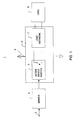
- FIG. 1 simplified block diagram of a generic switching power amplifier 6 designed into a conventional RF transmission system 1.
- the system includes a driver 4, the power amplifier 6, comprising a switch 5 and load network 7, and a load 8.
- the input signal 2 to be amplified is input to the driver stage 4, which controls the active device 5 in the amplifier.
- the active device acts substantially as a switch when appropriately driven by the driver and thus is represented as a single-pole, single throw switch.
- the active device is powered by a dc power supply 3, and has an output connected to the input of the load network 7.
- the output of the load network 7 is connected to the load 8, such as an antenna.
- the dc energy is converted into ac energy at this switching frequency and its harmonics.
- the load network 7 may employ one or more filters to control the power dissipation caused by switching action (i.e. the efficiency of the device), reduce the level of the harmonic overtones at the load, and/or provide impedance transformation.
- the design of the load network determines the behavior of the voltage and currents in the switching amplifier 6, and thus the class of operation by which the amplifier is denoted.
- the class E amplifier achieves high efficiency at high frequencies by essentially eliminating the dominant cause of the switching power dissipation that occurs in other types of switching amplifiers, namely the loss associated with capacitive discharge.
- a capacitance, C s shunts the power switch.
- this capacitance is the inherent parasitic capacitance, C out , of the circuit components (transistor) and wiring; the circuit designer might intentionally wish to add additional capacitance.
- this shunt capacitance is typically undesirable.
- the switch is turned on when the voltage across the switch and its shunt capacitance is nonzero, the energy stored in the charged capacitance will be dissipated as heat; the energy is C s V 2 / 2, where C s is the capacitance shunting the switch and V is the voltage across the switch (and hence across the capacitance) when the switch is turned on.
- the switching frequency is f o
- the power dissipation is C s V 2 f o / 2.
- the power dissipation is directly proportional to the switching frequency.
- this power dissipation can become a severe drawback, often becoming the dominant power loss mechanism.
- the switch is discharging this capacitor, the switch is subjected to both the capacitor voltage and the discharge current, simultaneously. If the simultaneous voltage and current are large enough, they can cause destructive failure and/or performance degradation of the power transistor.
- Zero-Voltage-Switching (ZVS) operation i.e. demanding that the voltage across the switch be substantially zero when the switch is turned on.
- ZVS Zero-Voltage-Switching
- class E operation achieves low power dissipation and low device stress by (a) incorporating the switch shunt capacitance as part of a network, allowing its detrimental effects to be accounted for and minimized and (b) using a resonant load network whose transient response after the switch turn-off brings the switch voltage back to zero (or nearly zero) at the time the switch will next be turned on.
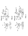
- a schematic of a typical class E amplifier circuit is shown in the simplified diagram of FIG. 2 .
- the power amplifier 10 includes a switching device 12 and a load network 20. DC power is supplied to the device 12 via a choke 14.
- the network includes a simple filter 24 which is connected in series to an RL load, represented by L L 26, and R L 28, respectively.
- the filter acts as a short circuit at the fundamental frequency, and an open circuit at all harmonics.
- the inherent shunt capacitance, C out , of the active device 12 e.g. between the anode and cathode of a three terminal transistor
- C s 22 which may include additional capacitance added by the designer.
- Class F is another well-known class of switching mode amplifiers.
- the class F amplifier derives its improved efficiency by using a multiple resonator load network to control the harmonic content of the active device's output voltage and/or current waveforms.
- the active device operates primarily as a switch and the load network, generally, is designed to yield short-circuit impedances at even harmonics of the fundamental frequency and to yield open-circuit impedances at odd harmonics of the fundamental frequency.
- Efficient operation of a class F amplifier is realized when the output voltage of the active device (transistor) is driven rapidly from saturation (low resistance) to cutoff (high resistance) voltage.
- the combination of the active device and the output network produces a half sine wave current when the device is saturated.
- a high Q resonant circuit for all odd harmonics up to the N th harmonic often consisting of several parallel LC filters, makes possible odd harmonic components in the output voltage by providing high impedances to the active device at these frequencies. These odd harmonic voltages sum with the fundamental frequency output voltage to effectively flatten the output voltage waveform. This results in a combination of higher efficiency and higher power output.
- resonant circuits are provided at all even harmonics up to the N th harmonic to short circuit the active device at these frequencies, thereby allowing the current waveform to approximate a half-sinusoid, further increasing the efficiency without any decrease in output power.
- a high Q filter circuit is tuned to the fundamental frequency to reject harmonics at the load and yield a sinusoidal output signal.
- the device's inherent parasitic capacitance must be kept small in order to avoid shorting the high impedance presented by the resonant circuit at the odd harmonics.
- class F is normally used only in applications where the transistor speed is relatively slow compared to the frequency of operation and using relatively small (i. e. low capacitance) devices, so that only a few harmonics need be tuned and so that the effect of the capacitance is small.
- a variation to the conventional class F amplifier is to invert the impedances at the harmonic overtones.
- the load network is designed to yield open circuit impedances at every even harmonic up to the N th harmonic and short circuit impedances at every odd harmonic up to the N th harmonic.
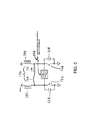
- Such an amplifier is called the inverse class-F, or class F -1 amplifier and one implementation is shown schematically in FIG. 3 .
- this class F -1 amplifier 40 includes a switching device 42 and load network 50 that comprises a filter 46 in series with the output of the switch and the resistive load 52 and a second filter 48 in parallel with the load 52.
- the series filter 46 presents relatively open circuit impedances for even harmonics and short circuit impedances for all other harmonics.
- the parallel filter 48 presents relatively short circuit impedances for all odd harmonics and open circuit impedances otherwise.
- This amplifier class has many of the benefits of class F, and additionally has the property of near-ZVS operation, although this quality is difficult to achieve in the presence of a large parasitic device capacitance C out .
- class F -1 has been largely ignored for many years, several recent works have shown that this class of operation compares favorably to class F using modem solid-state devices.
- class E and F power amplifier performances are compared, a significant advantage of a class E amplifier over a class F amplifier is its circuit topology, which incorporates the switching device output parasitic capacitance as part of its circuit.
- class E amplifiers do not lose power efficiency due to the charging and discharging of this parasitic capacitor as can occur in amplifier classes such as class F and class F -1 which do not account for the capacitor's effect, nor do they require elaborate resonant circuits to reduce the effect of this capacitance.
- the class E design is relatively simple, consisting of just a few components (at least one less filter than in the class F design).
- class E design receives the full promised benefits of its operating class with this simple circuit, whereas the class F and F -1 approaches must incorporate increasingly larger numbers of circuit elements in order to approach the ideal class F performance.
- class F amplifiers due to its anode (i.e., transistor drain or collector) voltage and current wave formats, class F amplifiers deliver significantly higher power and promise higher power-efficiency than class E amplifiers when they are using the same transistor under the same supply conditions.
- class F and F -1 circuits can be quite complex and can use many more components than class E devices.
- the present invention comprises a high efficiency switching power amplifier (100) for amplifying a high frequency input signal having at least one fundamental frequency, and adapted to drive a load, comprising:
- the hybrid class E/F load network is configured to present to the switching component of the active device, at all harmonic frequencies substantially present in at least one of the voltage and current waveforms of the active device, a substantially inductive load at each fundamental frequency, a substantially open circuit at a predetermined number, N E , of even harmonic overtones for each fundamental frequency up to an N th harmonic, a substantially short circuit at a predetermined number, N O , of odd harmonic overtones for each fundamental frequency up to an N th harmonic, and a substantially capacitive impedance load at the remaining harmonic overtones, up to an N th harmonic.
- the load network includes a two port filter network having an input port and an output port, the input port being connected to the active device in parallel with the parasitic output capacitance C out , and the output port being connected to the load.
- the load network may also be configured to provide wideband tuning of an input signal having a fundamental frequency range from f 1 to f 2 , where f 2 ⁇ 3 f 1 .
- the hybrid class E/F load network connected to the active device is configured to present to the active device a substantially open circuit at a predetermined number of even harmonic overtones of the fundamental frequency, a substantially short circuit at a predetermined number of odd harmonic overtones of the fundamental frequency, and a substantially capacitive impedance load at the remaining harmonic overtones.
- the hybrid class E/F load network is configured to present to the switching component, at all harmonic frequencies that are substantially present in at least one of the voltage and current waveforms of the active device, a substantially inductive load at each fundamental frequency of operation that results in substantially zero-voltage-switching (ZVS) operation of the active device, impedances substantially larger in magnitude than 1/(2 ⁇ fC s ) a at a predetermined number, N E , of even harmonic overtones of each fundamental frequency, impedances substantially smaller in magnitude than 1/(2 ⁇ fC S ) at a predetermined number, N O , of odd harmonic overtones of each fundamental frequency, and an impedance substantially equal to 1/j ⁇ C s at the remaining harmonic overtones of each fundamental frequency.
- ZVS substantially zero-voltage-switching
- C s C out + C added , where C added ⁇ 0, and N E ⁇ 0, N O ⁇ 0, and the total number of tuned harmonic overtones, N E + N O , is at least one and less than the total number of harmonic overtone frequencies substantially present in the active device's at least one of voltage and current waveforms. Since the network need not operate to provide substantially open and short circuits, as in the prior examples, the network can be simplified to a significant degree.
- a multiple active device high efficiency switching power amplifier for amplifying a high frequency input signal having at least one fundamental frequency and adapted to drive a load.
- a first high-speed active device having a parasitic output capacitance, C out1 and adapted to operate substantially as a switch and a second high-speed active device having a parasitic output capacitance, C out2 and adapted to operate substantially as a switch, are provided together with a hybrid three-port class E/F load network.
- the network has a first port connected to the first active device, a second port connected to the second active device, and a third port connected to the load, such that when the first and second active devices are driven in a push-pull configuration, the network presents to the switching component an effective input impedance that provides a substantially inductive load in series with the substantially resistive load at all fundamental frequencies; a substantially open circuit at one or more even harmonics for each fundamental frequency up to an N th harmonic, a substantially short circuit at one or more odd harmonics for each fundamental frequency up to an N th harmonic, and a substantially capacitive impedance load at the remaining harmonic overtones, up to an N th harmonic.
- the amplifier further includes a transformer connected to the outputs of the two active devices and the load such that the load is dc isolated from the outputs of the two active devices via the transformer.
- a quasi-class E/F 3 high efficiency amplifier for amplifying an input signal having at least one fundamental frequency and adapted to drive a load.
- This amplifier includes a high speed active device that comprises a switching component that operates substantially as a switch and a parasitic capacitance, C out , in parallel with the switching component and an LC parallel tank circuit that is resonant at the second harmonic of the fundamental frequency.
- the active device is connected in series to the load through the LC parallel tank circuit.
- a method of amplifying an RF signal with an active device switch includes amplifying the signal with an active device that comprises a switching component that operates substantially as a switch and a parasitic capacitance, C out , in parallel with the switching component.
- the method includes tuning the amplified signal to provide a substantially inductive load to the switching component at the fundamental frequency, tuning the amplified signal to provide a substantially open circuit to the active device at selected even harmonic overtones, tuning the amplified signal to provide a substantially short circuit to the active device at selected odd harmonic overtones; and providing substantially capacitive loading to the active device for the non-selected harmonic overtones.
- the network is configured to present to the switching component, at all harmonic frequencies substantially present in at least one of the voltage and current waveforms of the active device, a substantially inductive load at each fundamental frequency, a substantially open circuit at the 2 nd harmonic, and a substantially capacitive impedance load at the remaining harmonic overtones, up to an N th harmonic, where N ⁇ 3.
- the network is configured to present to the switching component, a substantially inductive load at each fundamental frequency; a substantially short circuit at the 3 rd harmonic, and a substantially capacitive impedance load at the remaining harmonic overtones, up to an N th harmonic where N ⁇ 3.
- the hybrid class E/F load network is configured to present to the switching component a substantially inductive load at each fundamental frequency, a substantially short circuit at the 3 rd harmonic, a substantially open circuit at the 2 nd harmonic, and a substantially capacitive impedance load at the remaining harmonic overtones, up to an N th harmonic, where N ⁇ 4.
- the hybrid class E/F load network is configured to present to the switching component a substantially inductive load at each fundamental frequency a substantially open circuit at the 4 th harmonic, and a substantially capacitive impedance load at the remaining harmonic overtones, up to an N th harmonic, where N ⁇ 4.
- the hybrid class E/F load network is configured to present to the switching component a substantially inductive load at each fundamental frequency a substantially open circuit at the 2 nd and 4 th harmonics, and a substantially capacitive impedance load at the remaining harmonic overtones, up to an N th harmonic, where N ⁇ 4.
- the hybrid class E/F load network is configured to present to the switching component a substantially inductive load at each fundamental frequency a substantially short circuit at the 3 rd harmonic, a substantially open circuit at the 4 th harmonic, and a substantially capacitive impedance load at the remaining harmonic overtones, up to an N th harmonic, where N ⁇ 4.
- the hybrid class E/F load network is configured to present to the switching component a substantially inductive load at each fundamental frequency a substantially short circuit at the 3 rd harmonic, a substantially open circuit at the 2 nd and 4 th harmonics, and a substantially capacitive impedance load at the remaining harmonic overtones, up to an N th harmonic, where N ⁇ 5.
- the hybrid class E/F load network is configured to present to the switching component a substantially inductive load at each fundamental frequency; a substantially short circuit at all odd harmonic overtones up to an N th harmonic, a substantially capacitive impedance load at the remaining harmonic overtones, up to an N th harmonic, where N ⁇ 5.
- the hybrid class E/F load network is configured to present to the switching component a substantially inductive load at each fundamental frequency a substantially short circuit at all odd harmonic overtones up to an N th harmonic, a substantially open circuit at a predetermined number, N E , of even harmonic overtones for each fundamental frequency up to an N th harmonic, a substantially capacitive impedance load at the remaining harmonic overtones, up to an N th harmonic, where N ⁇ 5 and 0 ⁇ N E ⁇ (N-2)/2.
- the present invention allows the achievement of higher performance than either the conventional class E or class F -1 amplifiers by incorporating some of the best features of both in a single design.
- the present invention employs the inductive-load phase correction technique of the class E amplifier to achieve ZVS switching conditions in the presence of a significant active device output capacitance, while simultaneously allowing some of the harmonic tuning benefits of the class F -1 amplifier.
- the invention allows the efficiency and output power of the active device to be improved by tuning some of the harmonics like a class-F -1 amplifier (i.e. open-circuit for even harmonics, short-circuit for odd harmonics), while allowing the remaining un-tuned harmonics to be capacitive as in a class-E amplifier.
- this tuning strategy allows the device capacitance to be easily incorporated into the circuit as in class-E, and the circuit can remain relatively simple since tuning circuits are required only for those harmonics tuned to open-circuit or short-circuit.
- the amplifiers of the present invention may approach 100% efficiency with a simple circuit consisting of a finite number of elements, whereas class-F and class-F -1 designs can only approach 100% as the number of harmonics tuned approaches infinity.
- the invention allows ZVS operation by tuning the fundamental frequency to present an inductive load (i.e.
- a load consisting of both an inductance and a resistance
- the inductance and resistance are appropriately sized relative to the capacitance C s so as to offset the capacitive effect of the un-tuned harmonics and bring the voltage to zero just before the switch closes each cycle.
- This inductance can be achieved by placing an appropriately-sized inductor in series with the load, but other solutions such as a shunt inductor or transmission line segments may also be used and are thus within the scope of the present invention.
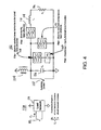
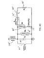
- the switching power amplifier 100 includes an active device.
- the active device comprises a switching component 102 that operates substantially as a switch (hereinafter the term “switch” will be used interchangeably with the term “switching component” to denote that portion of the active device that operates substantially as a switch) and a parasitic capacitance, C out , in parallel with the switching component.
- switch switching component
- C out parasitic capacitance
- the device is connected to an output circuit load network 110.
- the network includes an even harmonic filter 108 in series with a "negative capacitance" filter 107, which are in parallel with the switch 102 and the shunt capacitance, denoted as C s , 106 (which may equal C out , the switch's inherent capacitance or may be C out + added capacitance), an odd harmonic filter 111 also in parallel with the switch, a fundamental frequency filter 112 in series with the output of the switch and the load and added inductance L L 114 in series with the primarily resistive load 116.
- the even harmonic filter 108 presents a substantially short circuit at selected even harmonics and an open otherwise.
- the "negative capacitance" filter 107 having an impedance -1/j ⁇ Cs at these harmonics is in parallel with the shunt capacitance C s 106 with an impedance 1/j ⁇ Cs, and so the combined impedance of these two elements is substantially equal to an open-circuit.
- the odd harmonic filter 111 presents a short circuit at the selected odd harmonics and an open otherwise, short-circuiting the active device at these harmonics.
- the series fundamental frequency filter 112 presents to the switch a short circuit at the fundamental frequency and an open circuit otherwise.
- the phase-control inductance, denoted as inductor L L 114 is placed in series with the resistive load, denoted as resistor R L 116.
- class E/F amplifiers Power amplifiers using this novel technique and topology will be classified as class E/F amplifiers.
- This topology covers of a family of amplifiers, specific implementations may be denoted as class E/F n1,n2,n3,etc., wherein the various subscripts are numbers denoting the harmonics for which the amplifier's load network has class F -1 impedances.
- class E/F 2,3,5 would describe an amplifier with a load network presenting to the active device an inductive load at the fundamental, open circuit at the second harmonic, short circuit at the third and fifth harmonics, and a capacitive load for the remaining overtones.
- This new class of amplifiers are numerous and may include: (a) higher efficiency and/or output power when compared to a similar class E amplifier; (b) reduced circuit complexity with comparable or better efficiency and/or output power when compared to a similar class F or class F -1 amplifier; (c) reduced peak voltage relative to the DC voltage when compared to a similar class E amplifier; (d) reduced peak current relative to the DC current when compared to a similar class E amplifier; and (e) allows for the incorporation of the switch's parasitic capacitor into the circuit while simultaneously achieving zero voltage switching (ZVS), unlike a class F or class F -1 amplifier.
- ZVS zero voltage switching
- the class E/F switching power amplifier of the present invention may include a switching device connected to the output circuit presenting an inductive load at the fundamental frequency, an open circuit at selected even harmonic overtones up to N th harmonic, shorts to ground at selected odd harmonic overtones up to N th harmonic, and capacitive loads at the remaining overtones up to the N th harmonic.
- the impedances of the output circuit above N th harmonic may be any impedance where N is a number equal to or greater than 3.
- the advantages of the present invention are measured relative to the performance characteristics of conventional class E and class F (and/or F -1 ) power amplifiers. Although the performance is generally best when tuned-harmonics have been completely short-circuited or open-circuited, this condition is not usually possible to achieve in practice and the designer must be content with reducing or increasing the magnitude of the impedance as much as possible respectively.
- the present invention broadly contemplates load networks that present impedances other than those described in connection with FIG. 4 .
- phase 4 may be designed to present (a) impedances larger than those presented by class E amplifiers at selected even harmonic overtones (Z in > 1/j ⁇ Cs ) (but not necessarily infinite), (b) impedances that are smaller than those presented by class E amplifiers (Z in ⁇ 1/j ⁇ Cs ) at selected odd harmonic overtones (Zin), and class-E-like capacitive impedances (Z in ⁇ 1/j ⁇ Cs ) at the remaining overtones.
- the resistance and inductance of the inductive load at the fundamental frequency are selected so as to achieve ZVS switching conditions.
- Such amplifiers may be classified as "quasi-class E/F" power amplifiers.
- these amplifiers can be easier to design and implement than their similar class E/F amplifier counterparts shown in FIG. 4 as they can use fewer components and lower quality components. They may even provide better performance than "true" class E/F amplifiers for some applications, such as when design factors (e.g. available component sizes, low component quality factors, etc.) other than the active device efficiency and output power are motivating the requirements of the load network.
- design factors e.g. available component sizes, low component quality factors, etc.
- the novel circuit topology of the present invention may be implemented in a variety of circuits.
- Single-active-device designs such as shown in FIG. 4 can be used to implement E/F designs in a very straightforward manner.
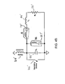
- a circuit such as shown in FIG. 4B may be employed.
- the circuit consists of the active device 102' in parallel with a shunt capacitance C S 106', to which are connected a series LC resonator 111' tuned to short-circuit the third harmonic, and an inductive load, through a second series LC resonator 112' tuned to resonate at the fundamental frequency.
- the inductive load consists of the load to be driven R L 116' and a phase-correction inductor L L 114'.
- a choke 104' provides connection to the dc power supply.
- the circuit satisfies the E/F 3 conditions by providing to the switch a short-circuiting at the third harmonic, an inductive load at the fundamental, and capacitive impedances at the remaining harmonics.
- the capacitance C S may not be an explicit component added by the designer, but may consist partially or entirely of the active device's parasitic output capacitance.
- FIG. 4C shows another example of a single-active-device design, in this case an E/F 2,3 implementation.
- This circuit consists of the active device 102" connected to a capacitance C S , and three resonant circuits.
- the first resonant circuit is a series LC filter 111" tuned to the third harmonic so as to short-circuit the active device at this frequency.
- the second is also a series LC resonator 113" tuned to the second harmonic, which is connected to the active device in series with an inductor 115 with a value of 1/4 ⁇ 0 2 C S .
- This circuit will provide the active device with an open-circuit at the second harmonic by resonating with the capacitance C S at this frequency.
- the third circuit is a series LC resonator 112" tuned to the fundamental frequency, to which is connected an inductive load consisting of an inductance L L 114" and the resistive load to be driven R L 116".
- a choke 104" provides connection to the dc power supply.
- FIG 4D shows an alternate implementation for E/F 2,3 using a dual-resonant filter network 118 to accomplish both second and third harmonic tunings.
- a filter can be implemented as shown in the figure using only two inductors L 1 and L 2 and one capacitor, C 1 .
- This network also passes dc currents, and so it can also replace the choke by placing it between the active device and the dc voltage supply.
- the fundamental frequency filter, shunt capacitance and load inductance are similar to the equivalent components in FIGS. 4B and 4C .
- the class E/F amplifier includes two switching devices 122, 126 connected in a push-pull configuration, each with a shunt capacitor 124, 128, respectively.
- Both an inductive load 130, represented by a resistor 132 and inductor 134, and a resonant circuit 140 are connected between the switches.
- the filter 140 acts (a) to short-circuit the two switches together for all odd harmonic overtones, (b) as an open circuit at the fundamental, and (c) has arbitrary impedances at the remaining overtones.
- one or more chokes 142, 144 may be placed in such a way as to allow direct current into both switches.
- the design, operation, and performance of the circuit shown in FIG. 5 follows the principles of two class E/F amplifiers connected in a push-pull configuration, each assisting the other in providing the appropriate harmonic tunings.
- Both switches are connected to the inductive load 130 at the fundamental frequency in classical push-pull fashion, making the impedance at this frequency on each switch equal to one half that of this inductive load.
- the odd harmonic overtones are short-circuited to each other through the filter, and therefore each is shorted to virtual ground due to the symmetric nature of the push-pull amplifier. This can be easily seen since the odd harmonics voltages of a push/pull amplifier's active devices must be 180° out-of-phase, thus if each is shorted to the other then both must be zero.
- the load and resonator are effectively removed from the circuit at the even harmonic overtones due to differential symmetry considerations, leaving each active device at these frequencies with a capacitive load consisting only of its shunt capacitance C S .
- C S capacitive load
- the even harmonic voltages of a push/pull amplifier are in-phase, thus the current through a differential load at these frequencies must be zero and the differential load will have no effect on the circuit for these harmonics.
- the circuit satisfies the conditions of class E/F amplification by providing short-circuits to the switch at all odd harmonics, capacitive load at all even harmonics, and inductive load at the fundamental.
- the amplifier has a load network supplying a class-F -1 impedance of short-circuit to ground at all odd harmonic overtones
- the denotation class E/F odd is suggested, where the odd subscript denotes that all odd harmonic overtones have been short-circuited.
- This circuit topology may offer several advantages. Using only a relatively small number of circuit components, this amplifier may be constructed with performance similar to a single-ended class E/F amplifier requiring many more components. The number of components is independent of the number of the order of odd harmonic overtones being tuned. A conventional single-ended implementation (i.e., a single-device switching amplifier) requires a larger number of tuned components proportional to the total number of the overtones being controlled.
- the resonator may be constructed using a simple parallel-connected LC resonator.
- the loaded Q of the LC parallel resonant circuit may be relatively low, even as low as one (although the third-harmonic in very low-Q cases is not very well shorted, making this case a quasi-class E/F design).
- This permits the use of very low unloaded-Q inductors allowing the use of this topology for applications like Si (silicon) substrate-based integrated circuits where any typical inductor presents a very low unloaded-Q of around 5, making the use of a low loaded-Q filter a necessity.
- a conventional approach using a class E or class F amplifier generally requires filters with loaded Q of at least 3.
- the series inductor in the load may be represented as an equivalent parallel inductor and incorporated into the LC tank, reducing the number of components further.
- FIG. 6 shows yet another novel circuit topology of a power amplifier circuit 150 that implements the class E/F amplifier with two switching devices 152, 156 connected in a push-pull configuration, each with a shunt capacitor 154, 158, respectively.
- a power amplifier circuit 150 that implements the class E/F amplifier with two switching devices 152, 156 connected in a push-pull configuration, each with a shunt capacitor 154, 158, respectively.
- the switches are both the primary 170 of a transformer and a resonant circuit 160 which short-circuits the two switches together for all odd harmonic overtones, presents an open circuit at the fundamental, and has arbitrary impedances at the remaining overtones.
- an RL load 162 Connected to the secondary 172 of the transformer is an RL load 162.
- a choke 174 (or more than one) is placed in such a way as to allow direct current into both switches.
- the load inductance 164 and the resonant circuit 160 may be connected on either side of the transformer, primary 170 or secondary 172 circuit, after proper impedance transformation. Additionally, the load inductance may also be incorporated into the resonator inductance. If desired, the parasitic inductances of the transformer may be used as elements in the resonant circuit 170 and for the load inductance 164, reducing the part count and allowing for the incorporation of transformer parasitics into the design.
- the output load is DC isolated from the switching circuit and supply;
- the output load may be connected in unbalanced mode; and
- the transformer turn ratio may be used to help match the switch output impedance to the load impedance.
- the present invention may use additional tuning circuits in parallel with each switch of the circuits shown in FIGS. 5 and 6 so as to selectively open circuit a number of even harmonic overtones.
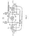
- FIG. 7 shows a schematic diagram of a circuit 180 for accomplishing this as well as a possible implementation strategy.
- additional circuits 210/212 and 220/222 which supply a suitable inductive impedance in parallel with the switching devices' 182 and 186 parallel capacitances 184 and 188, respectively, at various even harmonic overtones, the class E/F odd amplifier concept may be extended to allow also for the open-circuiting of any number of even harmonics, providing potential additional performance benefits.
- the present invention encompasses a virtually unlimited number of specific class E/F networks.
- the present invention specifically discloses several lower-order harmonic tuning networks. Specifically, these networks includes those that present: (a) a substantially open circuit at the 2 nd harmonic; (b) a substantially short circuit at the 3 rd harmonic, (c) a substantially short circuit at the 3 rd harmonic and a substantially open circuit at the 2 nd harmonic; (d) a substantially open circuit at the 4 th harmonic; (e) a substantially open circuit at the 2 nd and 4 th harmonics; (e) a substantially short circuit at the 3 rd harmonic and a substantially open circuit at the 4 th harmonic; (f) a substantially short circuit at the 3 rd harmonic and a substantially open circuit at the 2 nd and 4 th harmonics; (g) a substantially short circuit at all odd harmonic overtones up to the N th harmonic, where N is greater than or
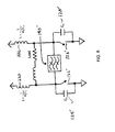
- circuit size and losses of the amplifier shown in FIG. 5 may be decreased by replacing the DC feed choke(s) with two inductors from the supply voltage to the respective switching devices: As shown in FIG. 8 , if each inductor, 230 232, is made to resonate at the second harmonic with the switching device's parallel capacitors C s , 124' and 128', respectively, the resulting class E/F 2,odd amplifier benefits from decreased switch losses and possibly reduced losses due to the choke's series resistance.
- a wideband class E/F odd switching amplifier may be constructed in such a way as to have class E/F odd impedances relative to the switch over a range of switching frequencies from f 1 to f 2 where f 2 ⁇ 3f 1 .
- the circuit consists of two switching devices connected in a push-pull configuration, each with a shunt capacitor, as shown in FIG. 5 . Between the switches are connected both a resistive load and a resonant circuit which short-circuits the two switches together for all frequencies greater than or equal to 3f 1 , and approximates the required inductance to meet the ZVS requirement from f 1 to f 2 .
- one or more chokes may be placed in such a way as to allow direct current into both switches. Constructed in this way, the circuit works as described in connection with FIG. 5 over the switching frequency range from f 1 to f 2 .
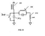
- FIG. 9 shows a novel implementation of a quasi class E/F 3 amplifier consisting of a switch or transistor 300 with parallel capacitor 302. They are connected to the supply through a choke 304.
- the switch or transistor is connected in series to the load 310 through an LC parallel resonant circuit 306 at the second harmonic.
- a filtering circuit may be added to avoid the higher order harmonic interference to the load, if the application requires it.
- this topology provides to the switch or transistor an inductive load at fundamental frequency, capacitive load at second harmonic, low impedance at third harmonic, and uncontrolled low impedances at higher order harmonics. This complies with requirements of quasi-class E/F amplifiers and offers several advantages.
- this modified quasi-class E/F circuit may be implemented using a relatively small number of components.
- Third, the loaded Q of the LC parallel resonant circuit may be very low and may be as low as one. This permits the use of very low unloaded Q inductors allowing the use of this topology for applications like Si (silicon) substrate based integrated circuits where any typical inductor presents a very low Q around 5.
- a conventional approach using class E or class F amplifiers requires inductors with loaded Q of at least 3.
- the resonant tank is a parallel LC rather than the typical series LC found in class E amplifiers, the inductance needed is reduced considerably. This is attractive when the size of the inductor is the limiting factor in reducing amplifier size and weight.
- the class E/F amplifier of the present invention may be tuned to operate in a linear mode, such as class A, class A/B, or class B at lower output power levels and E/F switching mode at higher output power levels.
- the output power and mode of operation may be varied by changing the input power and/or bias conditions.
- an amplifier may be constructed that has the high efficiency advantages of class E/F at the higher power levels while allowing the output power to be modulated or varied by changing drive conditions.
Landscapes
- Engineering & Computer Science (AREA)
- Power Engineering (AREA)
- Amplifiers (AREA)
Claims (19)
- Un amplificateur (100) de puissance de commutation à haute efficacité pour amplifier un signal d'entrée à haute fréquence, ayant au moins une fréquence fondamentale, et adapté pour commander une charge, comprenant :(a) un dispositif actif à haute vitesse, comprenant :un composant (102) de commutation qui, fonctionne sensiblement en tant que commutateur, etune capacité parasite, Cout, en parallèle avec le composant de commutation ; et(b) un réseau (110) de charge de classe E/F hybride connecté au dispositif actif, dans lequel le réseau (110) de charge de classe E/F hybride est configuré pour présenter au composant (102) de commutation :(i) une charge sensiblement inductive à la fréquence fondamentale de fonctionnement,(ii) un circuit sensiblement ouvert à un nombre prédéterminé de sons harmoniques d'ordre pair de la fréquence fondamentale,(iii) sensiblement un court-circuit à un nombre prédéterminé de sons harmoniques d'ordre impair de la fréquence fondamental, et(iv) une charge d' impédance sensiblement capacitive aux sons harmoniques restants.
- L'amplificateur selon la revendication 1, dans lequel le réseau est configuré pour présenter au composant (102) de commutation, à toutes les fréquences harmoniques sensiblement présentes dans au moins l'une des formes d'onde de tension et d'intensité du dispositif actif,(i) un circuit sensiblement ouvert à un nombre prédéterminé, NE, de sons harmoniques d'ordre pair pour chaque fréquence fondamentale, jusqu'à une N-ième harmonique,(ii) sensiblement un court-circuit à un nombre prédéterminé, No, de sons harmoniques d'ordre impair pour chaque fréquence fondamentale jusqu'à une N-ième harmonique, et(iii) une charge d'impédance sensiblement capacitive aux sons harmoniques restants, jusqu'à une N-ième harmonique, dans lequel N≥3 et 1≤NE + No≤N-2.
- L'amplificateur selon la revendication 2, dans lequel si NE = 1, alors No>0.
- L'amplificateur selon la revendication 2, dans lequel le réseau (110) de charge comprend un réseau à filtre à deux ports ayant un port d'entrée et un port de sortie, le port d'entrée étant connecté au dispositif actif et le port de sortie étant connecté à la charge.
- L'amplificateur selon la revendication 1, comprenant en outre :(a) un dispositif actif à haute vitesse, qui comprend :un composant de commutation qui fonctionne sensiblement en tant qu'un commutateur etune capacité parasite, Cout, en parallèle avec le composant de commutation ; et(b) un réseau de charge de classe E/F de classe hybride connecté au dispositif actif, dans lequel le réseau est configuré pour présenter au composant de commutation, à toutes les fréquences harmoniques qui sont sensiblement présentes dans au moins l'une des formes d'onde de tension et d'intensité du dispositif actif,dans lequel(i) une charge sensiblement inductive à chaque fréquence fondamentale de fonctionnement, qui donne un fonctionnement sensiblement à communication à tension zéro (ZVS) du dispositif actif,(ii) des impédances de valeur sensiblement supérieure à 1/(2πfCs) à un nombre prédéterminé, NE, de sons harmoniques d'ordre pair de chaque fréquence fondamentale,(iii) des impédances de valeur sensiblement inférieure à 1/(2πfCs) à un nombre prédéterminé, No, de sons harmoniques d'ordre impair de chaque fréquence fondamentale, et(iv) une impédance sensiblement égale à 1/ωCs aux sons harmoniques restants de chaque fréquence fondamentale,
Cs = Cout + Cadded où Cadded ≥ 0, et
NE ≥ 0, No≥0, et le nombre total de sons harmoniques accordés, NE + No, est d'au moins un et inférieur au nombre total des fréquences harmoniques sensiblement présentes dans au moins l'une des formes d'onde en tension et en intensité du dispositif actif. - L'amplificateur selon la revendication 1, comprenant en outre:(a) un premier dispositif actif à haute vitesse, comprenant :un composant de commutation fonctionnant sensiblement en tant que commutateur etune capacité parasite, Cout1, en parallèle avec le composant de commutation,(b) un deuxième dispositif actif à haute vitesse, qui comprend :un composant de commutation qui fonctionne sensiblement en tant que commutateur et une capacité parasite, Cout2, en parallèle avec le composant de commutation, et(c) un réseau de charge de classe E/F à trois portes hybride ayant :(i) un premier port connecté au premier dispositif actif,(ii) un deuxième port connecté au deuxième dispositif actif, et(iii) un troisième port connecté à la charge,de manière que, lorsque les premiers et les deuxièmes dispositifs actifs sont commandés en configuration symétrique, le réseau présente aux composants de commutation des dispositifs actifs une impédance d'entrée effective qui fournit(i) une charge sensiblement inductive en série avec la charge sensiblement résistive à toutes les fréquences fondamentales,(ii) un circuit sensiblement ouvert à une ou plusieurs harmoniques d'ordre pair pour chaque fréquence fondamentale jusqu'à une N-ième harmonique,(iii) sensiblement un court-circuit à une ou plusieurs harmoniques d'ordre impair pour chaque fréquence fondamentale jusqu'à une N-ième harmonique, et(iv) une charge d'impédance sensiblement capacitive aux sons harmoniques restants, jusqu'à une N-ième harmonique.
- L'amplificateur selon la revendication 6, comprenant en outre un transformateur couplé aux sorties des deux dispositifs actifs et à la charge de manière que la charge soit effectivement isolée vis-à-vis des sorties des deux dispositifs actifs via le transformateur.
- L'amplificateur selon la revendication 1, dans lequel le réseau (110) de charge est configuré pour fournir une syntonisation à large bande d'un signal d'entrée ayant une plage de fréquences fondamentales, allant de f 1, jusqu'à une fréquence telle que f 2≥f≥f 1 , où f 2<3f 1 .
- L'amplificateur selon la revendication 1, dans lequel le réseau est configuré pour présenter au composant (102) de commutation, à toutes les fréquences harmoniques sensiblement présentes dans au moins une des formes d'ondes de tension et d'intensité du dispositif actif,(i) une charge sensiblement inductive à chaque fréquence fondamentale;(ii) un circuit sensiblement ouvert à la deuxième harmonique, et(iii) une charge d'impédance sensiblement capacitive aux sons harmoniques restants, jusqu'à une N-ième harmonique,où N≥3.
- L'amplificateur selon la revendication 1, dans lequel le réseau est configuré pour présenter au composant (102) de commutation, à toutes les fréquences harmoniques sensiblement présentes dans au moins l'une des formes d'ondes de tension et d'intensité du dispositif actif,(i) une charge sensiblement inductive à chaque fréquence fondamentale;(ii) sensiblement un court-circuit à la troisième harmonique, et(iii) une charge d'impédance sensiblement capacitive aux sons harmoniques restants, jusqu'à une N-ième harmonique,dans lequel N≥3.
- L'amplificateur selon la revendication 1, dans lequel le réseau est configuré pour présenter au composant (102) de commutation, à toutes les fréquences harmoniques sensiblement présentes dans au moins une des formes d'ondes de tension et d'intensité du dispositif actif,(i) une charge sensiblement inductive à chaque fréquence fondamentale;(ii) sensiblement un court-circuit à la troisième harmonique,(iii) un circuit sensiblement ouvert à la deuxième harmonique, et(iv) une charge à impédance sensiblement capacitive aux sons harmoniques restants, jusqu'à une N-ième harmonique,dans lequel N≥4.
- L'amplificateur selon la revendication 1, dans lequel le réseau est configuré pour présenter au composant (102) de commutation, à toutes les fréquences harmoniques sensiblement présentes dans au moins une des formes d'ondes de tension et d'intensité du dispositif actif,(i) une charge sensiblement inductive à chaque fréquence fondamentale;(ii) un circuit sensiblement ouvert à la quatrième harmonique, et(iii) une charge sensiblement capacitive aux sons harmoniques restants, jusqu'à une N-ième harmonique,dans lequel N≥4.
- L'amplificateur selon la revendication 1, dans lequel le réseau est configuré pour présenter au composant (102) de commutation, à toutes les fréquences harmoniques sensiblement présentes dans au moins une des formes d'ondes de tension et d'intensité du dispositif actif,(i) une charge sensiblement inductive à chaque fréquence fondamentale ;(ii) un circuit sensiblement ouvert aux deuxième et quatrième harmoniques, et(iii) une charge d'impédance sensiblement capacitive aux sons harmoniques restants, jusqu'à une N-ième harmonique,dans lequel N≥4.
- L'amplificateur selon la revendication 1, dans lequel le réseau est configuré pour présenter au composant (102) de commutation, à toutes les fréquences harmoniques sensiblement présentes dans au moins une des formes d'ondes de tension et d'intensité du dispositif actif,(i) une charge sensiblement inductive à chaque fréquence fondamentale;(ii) sensiblement un court-circuit à la troisième harmonique,(iii) un circuit sensiblement ouvert à la quatrième harmonique, et(iv) une charge d'impédance sensiblement capacitive aux sons harmoniques restants, jusqu'à une N-ième harmonique,dans lequel N≥4.
- L'amplificateur selon la revendication 1, dans lequel le réseau est configuré pour présenter au composant (102) de commutation, à toutes les fréquences harmoniques sensiblement présentes dans au moins une des formes d'ondes de tension et d'intensité du dispositif actif,(i) une charge sensiblement inductive à chaque fréquence fondamentale ;(ii) sensiblement un court-circuit à la troisième harmonique(iii) un circuit sensiblement ouvert aux deuxième et quatrième harmoniques, et(iv) une charge d'impédance sensiblement capacitive aux sons harmoniques restants, jusqu'à une N-ième harmonique,dans lequel N≥5.
- L'amplificateur selon la revendication 1, dans lequel le réseau est configuré pour présenter au composant (102) de commutation, à toutes les fréquences harmoniques sensiblement présentes dans au moins une des formes d'ondes de tension et d'intensité du dispositif actif,(i) une charge sensiblement inductive à chaque fréquence fondamentale;(ii) sensiblement un court-circuit à la troisième harmonique(iii) un circuit sensiblement ouvert à tous les sons harmonique d'ordre impair jusqu'à une N-ième harmonique, et(iv) une charge d'impédance sensiblement capacitive aux sons harmoniques restants, jusqu'à une N-ième harmonique,dans lequel N≥5.
- L'amplificateur selon la revendication 1, dans lequel le réseau est configuré pour présenter au composant (102) de commutation, à toutes les fréquences harmoniques sensiblement présentes dans au moins une des formes d'ondes de tension et d'intensité du dispositif actif,(i) une charge sensiblement inductive à chaque fréquence fondamentale ;(ii) sensiblement un court-circuit à tous les sons harmonique d'ordre impair jusqu'à une N-ième harmonique,(iii) un circuit sensiblement ouvert à un nombre prédéterminé, NE, de sons harmoniques d'ordre pair pour chaque fréquence fondamentale jusqu'à une Nième harmonique,(iv) une charge à impédance sensiblement capacitive aux sons harmoniques restants, jusqu'à une N-ième harmonique,dans lequel N≥5 et 0≤NE≤(N-2)/2.
- L'amplificateur selon la revendication 1, comprenant en outre :(a) un dispositif actif à haute vitesse qui comprend un composant de commutation qui fonctionne sensiblement en tant que commutateur et une capacité parasite, Cout, en parallèle au composant de commutation, et(b) un circuit résonant parallèle LC qui est résonnant à la deuxième harmonique de la fréquence fondamentale,le dispositif actif étant banché en série à la charge par l'intermédiaire du circuit résonant parallèle LC.
- Un procédé d'utilisation en liaison avec l'amplificateur selon la revendication 1, comprenant :l'amplification du signal avec un dispositif actif à haute vitesse;la syntonisation du signal amplifié pour fournir une charge sensiblement inductive au dispositif actif à la fréquence fondamentale ;la syntonisation du signal amplifié pour fournir un circuit sensiblement ouvert dans le dispositif actif à des sons harmoniques d'ordre pair sélectionnés ;la syntonisation du signal amplifié pour fournir un circuit sensiblement ouvert dans le dispositif actif à des sons harmoniques d'ordre impair sélectionnés ; etla fourniture d'une charge sensiblement capacitive au dispositif actif pour les sons harmoniques non sélectionnés.
Applications Claiming Priority (3)
| Application Number | Priority Date | Filing Date | Title |
|---|---|---|---|
| US23947300P | 2000-10-10 | 2000-10-10 | |
| US239473P | 2000-10-10 | ||
| PCT/US2001/031808 WO2002031966A2 (fr) | 2000-10-10 | 2001-10-09 | Amplificateurs de puissance de commutation de classe e/f |
Publications (2)
| Publication Number | Publication Date |
|---|---|
| EP1344315A2 EP1344315A2 (fr) | 2003-09-17 |
| EP1344315B1 true EP1344315B1 (fr) | 2008-03-26 |
Family
ID=22902282
Family Applications (1)
| Application Number | Title | Priority Date | Filing Date |
|---|---|---|---|
| EP01981485A Expired - Lifetime EP1344315B1 (fr) | 2000-10-10 | 2001-10-09 | Amplificateurs de puissance de commutation de classe e/f |
Country Status (9)
| Country | Link |
|---|---|
| US (2) | US6724255B2 (fr) |
| EP (1) | EP1344315B1 (fr) |
| JP (2) | JP5255744B2 (fr) |
| KR (1) | KR100852314B1 (fr) |
| CN (1) | CN1295865C (fr) |
| AT (1) | ATE390755T1 (fr) |
| AU (1) | AU2002213122A1 (fr) |
| DE (1) | DE60133409T2 (fr) |
| WO (1) | WO2002031966A2 (fr) |
Cited By (1)
| Publication number | Priority date | Publication date | Assignee | Title |
|---|---|---|---|---|
| EP2752990A4 (fr) * | 2011-08-29 | 2015-07-08 | Univ Electro Communications | Amplificateur de puissance à haut rendement |
Families Citing this family (97)
| Publication number | Priority date | Publication date | Assignee | Title |
|---|---|---|---|---|
| US7180758B2 (en) * | 1999-07-22 | 2007-02-20 | Mks Instruments, Inc. | Class E amplifier with inductive clamp |
| US6856199B2 (en) * | 2000-10-10 | 2005-02-15 | California Institute Of Technology | Reconfigurable distributed active transformers |
| EP1400012B1 (fr) | 2000-10-10 | 2011-08-31 | California Institute Of Technology | Architecture repartie d'amplificateur de puissance a geometrie circulaire |
| US6577199B2 (en) * | 2000-12-07 | 2003-06-10 | Ericsson, Inc. | Harmonic matching network for a saturated amplifier |
| CN1625834B (zh) * | 2002-02-01 | 2010-05-26 | Nxp股份有限公司 | 半导体放大器元件的输出电路 |
| TWI326967B (en) | 2002-03-11 | 2010-07-01 | California Inst Of Techn | Differential amplifier |
| DE10211609B4 (de) * | 2002-03-12 | 2009-01-08 | Hüttinger Elektronik GmbH & Co. KG | Verfahren und Leistungsverstärker zur Erzeugung von sinusförmigen Hochfrequenzsignalen zum Betreiben einer Last |
| US6806767B2 (en) * | 2002-07-09 | 2004-10-19 | Anadigics, Inc. | Power amplifier with load switching circuit |
| US7555057B2 (en) * | 2003-01-17 | 2009-06-30 | Texas Instruments Incorporated | Predistortion calibration in a transceiver assembly |
| US6879209B2 (en) | 2003-07-08 | 2005-04-12 | Icefyre Semiconductor Corp. | Switched-mode power amplifier using lumped element impedance inverter for parallel combining |
| GB0404121D0 (en) * | 2004-02-25 | 2004-03-31 | Univ Belfast | Class E power amplifier circuit and associated transmitter circuits |
| JP4520204B2 (ja) * | 2004-04-14 | 2010-08-04 | 三菱電機株式会社 | 高周波電力増幅器 |
| US7660562B2 (en) * | 2004-06-21 | 2010-02-09 | M/A-Com Technology Solutions Holdings, Inc. | Combined matching and filter circuit |
| US7457380B2 (en) * | 2004-06-28 | 2008-11-25 | Broadcom Corporation | Low noise circuit and applications thereof |
| WO2006016299A1 (fr) * | 2004-08-09 | 2006-02-16 | Koninklijke Philips Electronics N.V. | Amplificateur integre de classe f a compensation de capacite de sortie parasite |
| US7355470B2 (en) | 2006-04-24 | 2008-04-08 | Parkervision, Inc. | Systems and methods of RF power transmission, modulation, and amplification, including embodiments for amplifier class transitioning |
| US7327803B2 (en) | 2004-10-22 | 2008-02-05 | Parkervision, Inc. | Systems and methods for vector power amplification |
| US7236053B2 (en) * | 2004-12-31 | 2007-06-26 | Cree, Inc. | High efficiency switch-mode power amplifier |
| US7345539B2 (en) * | 2005-02-10 | 2008-03-18 | Raytheon Company | Broadband microwave amplifier |
| US7315212B2 (en) * | 2005-04-13 | 2008-01-01 | International Business Machines Corporation | Circuits and methods for implementing transformer-coupled amplifiers at millimeter wave frequencies |
| US7265619B2 (en) * | 2005-07-06 | 2007-09-04 | Raytheon Company | Two stage microwave Class E power amplifier |
| US7548112B2 (en) * | 2005-07-21 | 2009-06-16 | Cree, Inc. | Switch mode power amplifier using MIS-HEMT with field plate extension |
| US7911272B2 (en) | 2007-06-19 | 2011-03-22 | Parkervision, Inc. | Systems and methods of RF power transmission, modulation, and amplification, including blended control embodiments |
| US8013675B2 (en) | 2007-06-19 | 2011-09-06 | Parkervision, Inc. | Combiner-less multiple input single output (MISO) amplification with blended control |
| US8334722B2 (en) | 2007-06-28 | 2012-12-18 | Parkervision, Inc. | Systems and methods of RF power transmission, modulation and amplification |
| US7411458B2 (en) | 2006-02-01 | 2008-08-12 | Motorola, Inc. | Method and apparatus for controlling an output voltage in a power amplifier |
| EP1985012B1 (fr) * | 2006-02-10 | 2011-06-29 | Nxp B.V. | Amplificateur de puissance |
| US7937106B2 (en) | 2006-04-24 | 2011-05-03 | ParkerVision, Inc, | Systems and methods of RF power transmission, modulation, and amplification, including architectural embodiments of same |
| US8031804B2 (en) | 2006-04-24 | 2011-10-04 | Parkervision, Inc. | Systems and methods of RF tower transmission, modulation, and amplification, including embodiments for compensating for waveform distortion |
| DE102006019887B4 (de) * | 2006-04-28 | 2012-09-27 | Infineon Technologies Ag | Multifunktions-RF-Schaltung |
| JP4257346B2 (ja) * | 2006-06-27 | 2009-04-22 | 株式会社東芝 | 電力増幅器 |
| US8315336B2 (en) | 2007-05-18 | 2012-11-20 | Parkervision, Inc. | Systems and methods of RF power transmission, modulation, and amplification, including a switching stage embodiment |
| JP5085179B2 (ja) | 2007-04-12 | 2012-11-28 | 株式会社東芝 | F級増幅回路 |
| EP2165415A4 (fr) * | 2007-07-05 | 2010-12-15 | Ericsson Telefon Ab L M | Dispositif d'amplification amélioré |
| US7710197B2 (en) * | 2007-07-11 | 2010-05-04 | Axiom Microdevices, Inc. | Low offset envelope detector and method of use |
| US7489202B1 (en) | 2007-08-20 | 2009-02-10 | Freescale Semiconductor, Inc. | RF amplifier with stacked transistors, transmitting device, and method therefor |
| JP2009081605A (ja) * | 2007-09-26 | 2009-04-16 | Univ Of Electro-Communications | 逆f級増幅回路 |
| JP2009130472A (ja) * | 2007-11-20 | 2009-06-11 | Univ Of Electro-Communications | 逆f級増幅回路 |
| US7760018B2 (en) * | 2007-12-31 | 2010-07-20 | Tialinx, Inc. | High-efficiency switching power amplifiers with low harmonic distortion |
| US7560994B1 (en) * | 2008-01-03 | 2009-07-14 | Samsung Electro-Mechanics Company | Systems and methods for cascode switching power amplifiers |
| US7746173B1 (en) * | 2008-04-30 | 2010-06-29 | Triquint Semiconductor, Inc. | Power amplifier with output harmonic resonators |
| WO2009145887A1 (fr) | 2008-05-27 | 2009-12-03 | Parkervision, Inc. | Systèmes et procédés de transmission, de modulation et d'amplification de puissance radioélectrique (rf) |
| WO2009149464A2 (fr) * | 2008-06-06 | 2009-12-10 | University Of Florida Research Foundation, Inc. | Procédé et appareil de transfert de puissance sans contact |
| CN104953965B (zh) * | 2008-09-01 | 2018-07-24 | 艾利森电话股份有限公司 | 混合类放大器 |
| US8054135B2 (en) * | 2008-12-05 | 2011-11-08 | General Electric Company | Class-E amplifier and lighting ballast using the amplifier |
| KR101042311B1 (ko) * | 2009-01-15 | 2011-06-17 | 금오공과대학교 산학협력단 | 가변 역 e-급 증폭기 |
| WO2011030264A1 (fr) * | 2009-09-09 | 2011-03-17 | Koninklijke Philips Electronics N.V. | Fonctionnement d'une lampe à décharge sans électrode |
| US8772975B2 (en) | 2009-12-07 | 2014-07-08 | Qualcomm Incorporated | Apparatus and method for implementing a differential drive amplifier and a coil arrangement |
| US8289085B2 (en) * | 2009-12-16 | 2012-10-16 | Auriga Measurement Systems, LLC | Amplifier circuit |
| US8344801B2 (en) * | 2010-04-02 | 2013-01-01 | Mks Instruments, Inc. | Variable class characteristic amplifier |
| WO2012000129A1 (fr) | 2010-06-29 | 2012-01-05 | Telefonaktiebolaget L M Ericsson (Publ) | Amplificateur de puissance multibande |
| KR101314145B1 (ko) * | 2010-09-02 | 2013-10-04 | 삼성전자주식회사 | 공진 전력 전송 시스템의 전력 변환기 및 공진 전력 전송 장치 |
| WO2012040879A1 (fr) * | 2010-09-30 | 2012-04-05 | Telefonaktiebolaget Lm Ericsson (Publ) | Amplificateur de puissance multi-bande en mode commuté |
| US9431975B2 (en) | 2011-04-04 | 2016-08-30 | The Trustees Of Columbia University In The City Of New York | Circuits for providing class-E power amplifiers |
| KR20140026458A (ko) | 2011-04-08 | 2014-03-05 | 파커비전, 인크. | Rf 전력 송신, 변조 및 증폭 시스템들 및 방법들 |
| KR20140034895A (ko) | 2011-06-02 | 2014-03-20 | 파커비전, 인크. | 안테나 제어 |
| US9083291B2 (en) * | 2011-08-12 | 2015-07-14 | Bae Systems Information And Electronic Systems Integration Inc. | Low voltage high efficiency gallium arsenide power amplifier |
| US8736368B2 (en) * | 2011-08-16 | 2014-05-27 | Qualcomm Incorporated | Class E amplifier overload detection and prevention |
| US8717102B2 (en) * | 2011-09-27 | 2014-05-06 | Infineon Technologies Ag | RF device with compensatory resonator matching topology |
| JP5773364B2 (ja) * | 2011-11-09 | 2015-09-02 | 国立大学法人 千葉大学 | Em級増幅器 |
| JP6156148B2 (ja) * | 2011-11-17 | 2017-07-05 | 日本電気株式会社 | 逆f級増幅回路及び逆f級増幅回路の寄生回路補償方法 |
| US8816769B2 (en) * | 2012-07-31 | 2014-08-26 | Intel Mobile Communications GmbH | Differential stacked output stage for power amplifiers |
| GB201215152D0 (en) | 2012-08-24 | 2012-10-10 | Imp Innovations Ltd | Maximising DC to load efficiency for inductive power transfer |
| GB201303849D0 (en) * | 2012-12-31 | 2013-04-17 | Continental Automotive Systems | Tuned power amplifier with multiple loaded chokes for inductively heated fuel injectors |
| GB201301208D0 (en) * | 2012-12-31 | 2013-03-06 | Continental Automotive Systems | Turned power amplifier with loaded choke for inductively heated fuel injector |
| CN103337964A (zh) * | 2013-04-27 | 2013-10-02 | 南京航空航天大学 | 一种超高频隔离推挽谐振功率变换器 |
| US9024691B2 (en) * | 2013-05-17 | 2015-05-05 | Georgia Tech Research Corporation | Adaptive power amplifier and methods of making same |
| GB201321267D0 (en) | 2013-12-02 | 2014-01-15 | Imp Innovations Ltd | Inductive power transfer system |
| KR20160058855A (ko) | 2013-09-17 | 2016-05-25 | 파커비전, 인크. | 정보를 포함하는 시간의 함수를 렌더링하기 위한 방법, 장치 및 시스템 |
| CN103684271A (zh) * | 2013-11-22 | 2014-03-26 | 小米科技有限责任公司 | 提高射频功率放大器效率的装置和方法 |
| US10063197B2 (en) | 2014-03-05 | 2018-08-28 | The Trustees Of Columbia University In The City Of New York | Circuits for power-combined power amplifier arrays |
| US9503025B2 (en) | 2014-07-11 | 2016-11-22 | Skyworks Solutions, Inc. | Power amplifier with termination circuit and resonant circuit |
| CN105471393B (zh) * | 2014-09-12 | 2018-12-18 | 通用电气公司 | 以零电压开关及热平衡控制算法运作的开关放大器 |
| US9614541B2 (en) | 2014-10-01 | 2017-04-04 | The Trustees Of Columbia University In The City Of New York | Wireless-transmitter circuits including power digital-to-amplitude converters |
| EP3202032B1 (fr) * | 2014-10-03 | 2021-09-22 | Short Circuit Technologies LLC | Separateur de frequence pour signaux rf pour un amplificateur de puissance e/f2 de classe à large bande 60 ghz |
| JP6336504B2 (ja) * | 2015-03-31 | 2018-06-06 | スカイワークス ソリューションズ, インコーポレイテッドSkyworks Solutions, Inc. | 多重帯域電力増幅器 |
| CN104953966B (zh) * | 2015-06-16 | 2018-05-18 | 深圳市华讯方舟微电子科技有限公司 | 一种e类功率放大器的补偿电路及其器件参数获取方法 |
| CN105048971B (zh) * | 2015-09-11 | 2019-03-08 | 上海无线电设备研究所 | 基于开关谐振结构的高效率Doherty功率放大器实现方法 |
| US9929704B2 (en) * | 2015-12-14 | 2018-03-27 | Qualcomm Incorporated | Class E2 amplifier |
| US10170940B2 (en) * | 2016-05-04 | 2019-01-01 | Imperial Innovations Limited | Wireless power transfer system |
| US9673766B1 (en) * | 2016-05-18 | 2017-06-06 | Nxp Usa, Inc. | Class F amplifiers using resonant circuits in an output matching network |
| JP2017208729A (ja) | 2016-05-19 | 2017-11-24 | 株式会社村田製作所 | 電力増幅モジュール |
| JP6787071B2 (ja) * | 2016-11-21 | 2020-11-18 | Tdk株式会社 | 電力変換装置 |
| DE102017208917A1 (de) * | 2017-05-26 | 2018-11-29 | TRUMPF Hüttinger GmbH + Co. KG | Hochfrequenzverstärkeranordnung und Verfahren zur Auslegung einer Hochfrequenzverstärkeranordnung |
| JP6812911B2 (ja) * | 2017-06-22 | 2021-01-13 | Tdk株式会社 | 電力変換装置 |
| US10381988B2 (en) * | 2017-09-15 | 2019-08-13 | Qualcomm Incorporated | Methods and apparatuses for ruggedizing a power amplifier against breakdown using harmonic tuning |
| US10714985B2 (en) * | 2017-10-11 | 2020-07-14 | Spark Connected LLC | Wireless power transfer system and method |
| JP6937432B2 (ja) | 2018-04-20 | 2021-09-22 | 日産自動車株式会社 | 共振型電力変換装置の制御方法および共振型電力変換装置 |
| EP3562036B1 (fr) * | 2018-04-26 | 2021-02-24 | Nxp B.V. | Amplificateur de puissance |
| CN108923755B (zh) * | 2018-06-12 | 2022-01-28 | 合肥工业大学 | 一种带减压负载电路的小直流馈电电感e类功率放大器 |
| US10784821B2 (en) | 2018-12-19 | 2020-09-22 | Nxp Usa, Inc. | High power radio frequency amplifiers and methods of manufacture thereof |
| US10784822B2 (en) * | 2018-12-19 | 2020-09-22 | Nxp Usa, Inc. | High power radio frequency amplifiers and methods of manufacture thereof |
| US11515123B2 (en) * | 2018-12-21 | 2022-11-29 | Advanced Energy Industries, Inc. | Apparatus and system for modulated plasma systems |
| KR102501647B1 (ko) | 2019-01-10 | 2023-02-20 | 삼성전자 주식회사 | 출력단에서 발생하는 로컬 주파수 신호를 감소시키기 위한 믹서 |
| US11469724B2 (en) * | 2020-11-09 | 2022-10-11 | Aira, Inc. | Free-boost class-e amplifier |
| WO2022265728A2 (fr) * | 2021-04-25 | 2022-12-22 | University Of Southern California | Amplificateur de puissance de classe ef à ondes millimétriques avec réglage simultané des harmoniques et des sous-harmoniques |
| CN118157598A (zh) * | 2024-03-29 | 2024-06-07 | 上海励兆科技有限公司 | 基于并联谐振单元的功放电路 |
Family Cites Families (24)
| Publication number | Priority date | Publication date | Assignee | Title |
|---|---|---|---|---|
| US3430157A (en) | 1966-11-10 | 1969-02-25 | John W Wood | High efficiency class c amplifier |
| US3919656A (en) | 1973-04-23 | 1975-11-11 | Nathan O Sokal | High-efficiency tuned switching power amplifier |
| US4667305A (en) * | 1982-06-30 | 1987-05-19 | International Business Machines Corporation | Circuits for accessing a variable width data bus with a variable width data field |
| US4607323A (en) | 1984-04-17 | 1986-08-19 | Sokal Nathan O | Class E high-frequency high-efficiency dc/dc power converter |
| US4644532A (en) * | 1985-06-10 | 1987-02-17 | International Business Machines Corporation | Automatic update of topology in a hybrid network |
| US4717884A (en) | 1986-04-14 | 1988-01-05 | Motorola, Inc. | High efficiency RF power amplifier |
| JPH0682998B2 (ja) * | 1986-07-30 | 1994-10-19 | 日本電信電話株式会社 | 電力増幅器 |
| US4747100A (en) * | 1986-08-11 | 1988-05-24 | Allen-Bradley Company, Inc. | Token passing network utilizing active node table |
| US4864563A (en) * | 1989-01-09 | 1989-09-05 | E-Systems, Inc. | Method for establishing and maintaining a nodal network in a communication system |
| US5276912A (en) * | 1990-02-06 | 1994-01-04 | Motorola, Inc. | Radio frequency power amplifier having variable output power |
| JPH0732335B2 (ja) | 1990-11-16 | 1995-04-10 | 日本電信電話株式会社 | 高周波増幅器 |
| CA2137289A1 (fr) * | 1992-06-05 | 1993-12-23 | Derek Bray | Lampe a decharge sans electrode comportant un amplificateur classe e symetrique et une bobine bifilaire |
| US5327337A (en) * | 1992-09-01 | 1994-07-05 | Broadcast Electronics, Inc. | Resonant push-pull switching power amplifier |
| JP2831257B2 (ja) * | 1994-01-26 | 1998-12-02 | 松下電工株式会社 | E級プッシュプル電力増幅回路 |
| JP2616464B2 (ja) * | 1994-10-31 | 1997-06-04 | 日本電気株式会社 | 高効率電力増幅回路 |
| JPH08148949A (ja) * | 1994-11-18 | 1996-06-07 | Fujitsu Ltd | 高周波増幅器 |
| JP3145640B2 (ja) * | 1996-08-16 | 2001-03-12 | 日本無線株式会社 | スイッチング電力増幅器 |
| DE19731691C1 (de) * | 1997-07-23 | 1998-10-08 | Siemens Ag | Leistungs-Schaltverstärker |
| JPH1146122A (ja) * | 1997-07-28 | 1999-02-16 | Japan Radio Co Ltd | スイッチング電力増幅回路 |
| US5969575A (en) * | 1997-12-11 | 1999-10-19 | Alcatel | Class A/F amplifier having second and third order harmonic input and output filtering and self bias distortion correction |
| JP2002510927A (ja) * | 1998-04-02 | 2002-04-09 | エリクソン インコーポレイテッド | Chireix/dohertyハイブリッド増幅器の電力波形合成 |
| US6285251B1 (en) * | 1998-04-02 | 2001-09-04 | Ericsson Inc. | Amplification systems and methods using fixed and modulated power supply voltages and buck-boost control |
| JP3888785B2 (ja) * | 1998-09-28 | 2007-03-07 | 三菱電機株式会社 | 高周波電力増幅器 |
| US6232841B1 (en) * | 1999-07-01 | 2001-05-15 | Rockwell Science Center, Llc | Integrated tunable high efficiency power amplifier |
-
2001
- 2001-10-09 EP EP01981485A patent/EP1344315B1/fr not_active Expired - Lifetime
- 2001-10-09 AT AT01981485T patent/ATE390755T1/de not_active IP Right Cessation
- 2001-10-09 WO PCT/US2001/031808 patent/WO2002031966A2/fr active Search and Examination
- 2001-10-09 KR KR1020037005090A patent/KR100852314B1/ko active IP Right Grant
- 2001-10-09 DE DE60133409T patent/DE60133409T2/de not_active Expired - Lifetime
- 2001-10-09 JP JP2002535249A patent/JP5255744B2/ja not_active Expired - Lifetime
- 2001-10-09 AU AU2002213122A patent/AU2002213122A1/en not_active Abandoned
- 2001-10-09 CN CNB018203396A patent/CN1295865C/zh not_active Expired - Lifetime
- 2001-10-09 US US09/974,557 patent/US6724255B2/en not_active Expired - Lifetime
-
2003
- 2003-11-18 US US10/715,696 patent/US6784732B2/en not_active Expired - Lifetime
-
2010
- 2010-12-28 JP JP2010292272A patent/JP5318083B2/ja not_active Expired - Lifetime
Cited By (2)
| Publication number | Priority date | Publication date | Assignee | Title |
|---|---|---|---|---|
| EP2752990A4 (fr) * | 2011-08-29 | 2015-07-08 | Univ Electro Communications | Amplificateur de puissance à haut rendement |
| US9257948B2 (en) | 2011-08-29 | 2016-02-09 | The University Of Electro-Communications | High efficiency power amplifier |
Also Published As
| Publication number | Publication date |
|---|---|
| US20040113689A1 (en) | 2004-06-17 |
| US6724255B2 (en) | 2004-04-20 |
| KR100852314B1 (ko) | 2008-08-18 |
| US6784732B2 (en) | 2004-08-31 |
| AU2002213122A1 (en) | 2002-04-22 |
| JP5318083B2 (ja) | 2013-10-16 |
| ATE390755T1 (de) | 2008-04-15 |
| WO2002031966A3 (fr) | 2002-08-08 |
| CN1479969A (zh) | 2004-03-03 |
| US20020101284A1 (en) | 2002-08-01 |
| WO2002031966A2 (fr) | 2002-04-18 |
| KR20040004398A (ko) | 2004-01-13 |
| JP5255744B2 (ja) | 2013-08-07 |
| EP1344315A2 (fr) | 2003-09-17 |
| CN1295865C (zh) | 2007-01-17 |
| DE60133409D1 (de) | 2008-05-08 |
| JP2011101408A (ja) | 2011-05-19 |
| JP2004520730A (ja) | 2004-07-08 |
| DE60133409T2 (de) | 2008-07-24 |
Similar Documents
| Publication | Publication Date | Title |
|---|---|---|
| EP1344315B1 (fr) | Amplificateurs de puissance de commutation de classe e/f | |
| JP2011101408A5 (fr) | ||
| CN1160850C (zh) | 用于开关式射频功率放大器的激励电路 | |
| US9306517B1 (en) | Resonant pre-driver for switching amplifier | |
| JP4954202B2 (ja) | ミリメートル波用途の電力増幅器の実施のための回路及び方法 | |
| US9806673B2 (en) | Class-E outphasing power amplifier with efficiency and output power enhancement circuits and method | |
| JP5711354B2 (ja) | クラス特性可変増幅器 | |
| US7265618B1 (en) | RF power amplifier having high power-added efficiency | |
| JP4808814B2 (ja) | パワー変換のためのスイッチング式インバータ及びコンバータ | |
| US20070222523A1 (en) | Multi-stage power amplifier with enhanced efficiency | |
| US7619469B2 (en) | Current switched circuit for switch mode power amplifiers | |
| CN220139528U (zh) | 射频功率放大器和射频前端模组 | |
| CN1437318A (zh) | 传输线调谐开关功率放大器 | |
| Salem et al. | A recursive house-of-cards digital power amplifier employing a λ/4-less Doherty power combiner in 65nm CMOS | |
| US8723601B2 (en) | Amplifier | |
| Hajimiri et al. | Class E/F switching power amplifiers | |
| Mariappan et al. | A 1.1-to-2.7 GHz CMOS Power Amplifier with Digitally-Reconfigurable-Impedance Matching-Network (DRIMN) for Wideband Performance optimization | |
| CN118740075A (zh) | 射频功率放大器和射频前端模组 |
Legal Events
| Date | Code | Title | Description |
|---|---|---|---|
| PUAI | Public reference made under article 153(3) epc to a published international application that has entered the european phase |
Free format text: ORIGINAL CODE: 0009012 |
|
| 17P | Request for examination filed |
Effective date: 20030508 |
|
| AK | Designated contracting states |
Kind code of ref document: A2 Designated state(s): AT BE CH CY DE DK ES FI FR GB GR IE IT LI LU MC NL PT SE TR |
|
| AX | Request for extension of the european patent |
Extension state: AL LT LV MK RO SI |
|
| 17Q | First examination report despatched |
Effective date: 20040820 |
|
| GRAP | Despatch of communication of intention to grant a patent |
Free format text: ORIGINAL CODE: EPIDOSNIGR1 |
|
| GRAS | Grant fee paid |
Free format text: ORIGINAL CODE: EPIDOSNIGR3 |
|
| GRAA | (expected) grant |
Free format text: ORIGINAL CODE: 0009210 |
|
| AK | Designated contracting states |
Kind code of ref document: B1 Designated state(s): AT BE CH CY DE DK ES FI FR GB GR IE IT LI LU MC NL PT SE TR |
|
| REG | Reference to a national code |
Ref country code: GB Ref legal event code: FG4D |
|
| REG | Reference to a national code |
Ref country code: CH Ref legal event code: EP Ref country code: IE Ref legal event code: FG4D |
|
| REF | Corresponds to: |
Ref document number: 60133409 Country of ref document: DE Date of ref document: 20080508 Kind code of ref document: P |
|
| PG25 | Lapsed in a contracting state [announced via postgrant information from national office to epo] |
Ref country code: FI Free format text: LAPSE BECAUSE OF FAILURE TO SUBMIT A TRANSLATION OF THE DESCRIPTION OR TO PAY THE FEE WITHIN THE PRESCRIBED TIME-LIMIT Effective date: 20080326 |
|
| PG25 | Lapsed in a contracting state [announced via postgrant information from national office to epo] |
Ref country code: AT Free format text: LAPSE BECAUSE OF FAILURE TO SUBMIT A TRANSLATION OF THE DESCRIPTION OR TO PAY THE FEE WITHIN THE PRESCRIBED TIME-LIMIT Effective date: 20080326 |
|
| NLV1 | Nl: lapsed or annulled due to failure to fulfill the requirements of art. 29p and 29m of the patents act | ||
| PG25 | Lapsed in a contracting state [announced via postgrant information from national office to epo] |
Ref country code: BE Free format text: LAPSE BECAUSE OF FAILURE TO SUBMIT A TRANSLATION OF THE DESCRIPTION OR TO PAY THE FEE WITHIN THE PRESCRIBED TIME-LIMIT Effective date: 20080326 |
|
| PG25 | Lapsed in a contracting state [announced via postgrant information from national office to epo] |
Ref country code: PT Free format text: LAPSE BECAUSE OF FAILURE TO SUBMIT A TRANSLATION OF THE DESCRIPTION OR TO PAY THE FEE WITHIN THE PRESCRIBED TIME-LIMIT Effective date: 20080901 Ref country code: SE Free format text: LAPSE BECAUSE OF FAILURE TO SUBMIT A TRANSLATION OF THE DESCRIPTION OR TO PAY THE FEE WITHIN THE PRESCRIBED TIME-LIMIT Effective date: 20080626 Ref country code: ES Free format text: LAPSE BECAUSE OF FAILURE TO SUBMIT A TRANSLATION OF THE DESCRIPTION OR TO PAY THE FEE WITHIN THE PRESCRIBED TIME-LIMIT Effective date: 20080707 |
|
| PG25 | Lapsed in a contracting state [announced via postgrant information from national office to epo] |
Ref country code: NL Free format text: LAPSE BECAUSE OF FAILURE TO SUBMIT A TRANSLATION OF THE DESCRIPTION OR TO PAY THE FEE WITHIN THE PRESCRIBED TIME-LIMIT Effective date: 20080326 |
|
| EN | Fr: translation not filed | ||
| PG25 | Lapsed in a contracting state [announced via postgrant information from national office to epo] |
Ref country code: DK Free format text: LAPSE BECAUSE OF FAILURE TO SUBMIT A TRANSLATION OF THE DESCRIPTION OR TO PAY THE FEE WITHIN THE PRESCRIBED TIME-LIMIT Effective date: 20080326 |
|
| PLBE | No opposition filed within time limit |
Free format text: ORIGINAL CODE: 0009261 |
|
| STAA | Information on the status of an ep patent application or granted ep patent |
Free format text: STATUS: NO OPPOSITION FILED WITHIN TIME LIMIT |
|
| 26N | No opposition filed |
Effective date: 20081230 |
|
| PG25 | Lapsed in a contracting state [announced via postgrant information from national office to epo] |
Ref country code: FR Free format text: LAPSE BECAUSE OF FAILURE TO SUBMIT A TRANSLATION OF THE DESCRIPTION OR TO PAY THE FEE WITHIN THE PRESCRIBED TIME-LIMIT Effective date: 20090116 |
|
| PG25 | Lapsed in a contracting state [announced via postgrant information from national office to epo] |
Ref country code: MC Free format text: LAPSE BECAUSE OF NON-PAYMENT OF DUE FEES Effective date: 20081031 |
|
| REG | Reference to a national code |
Ref country code: CH Ref legal event code: PL |
|
| PG25 | Lapsed in a contracting state [announced via postgrant information from national office to epo] |
Ref country code: IT Free format text: LAPSE BECAUSE OF FAILURE TO SUBMIT A TRANSLATION OF THE DESCRIPTION OR TO PAY THE FEE WITHIN THE PRESCRIBED TIME-LIMIT Effective date: 20080326 |
|
| PG25 | Lapsed in a contracting state [announced via postgrant information from national office to epo] |
Ref country code: CY Free format text: LAPSE BECAUSE OF FAILURE TO SUBMIT A TRANSLATION OF THE DESCRIPTION OR TO PAY THE FEE WITHIN THE PRESCRIBED TIME-LIMIT Effective date: 20080326 |
|
| PG25 | Lapsed in a contracting state [announced via postgrant information from national office to epo] |
Ref country code: CH Free format text: LAPSE BECAUSE OF NON-PAYMENT OF DUE FEES Effective date: 20081031 Ref country code: IE Free format text: LAPSE BECAUSE OF NON-PAYMENT OF DUE FEES Effective date: 20081009 Ref country code: LI Free format text: LAPSE BECAUSE OF NON-PAYMENT OF DUE FEES Effective date: 20081031 |
|
| PG25 | Lapsed in a contracting state [announced via postgrant information from national office to epo] |
Ref country code: LU Free format text: LAPSE BECAUSE OF NON-PAYMENT OF DUE FEES Effective date: 20081009 |
|
| PG25 | Lapsed in a contracting state [announced via postgrant information from national office to epo] |
Ref country code: TR Free format text: LAPSE BECAUSE OF FAILURE TO SUBMIT A TRANSLATION OF THE DESCRIPTION OR TO PAY THE FEE WITHIN THE PRESCRIBED TIME-LIMIT Effective date: 20080326 |
|
| PG25 | Lapsed in a contracting state [announced via postgrant information from national office to epo] |
Ref country code: GR Free format text: LAPSE BECAUSE OF FAILURE TO SUBMIT A TRANSLATION OF THE DESCRIPTION OR TO PAY THE FEE WITHIN THE PRESCRIBED TIME-LIMIT Effective date: 20080627 |
|
| PGFP | Annual fee paid to national office [announced via postgrant information from national office to epo] |
Ref country code: DE Payment date: 20201028 Year of fee payment: 20 Ref country code: GB Payment date: 20201027 Year of fee payment: 20 |
|
| REG | Reference to a national code |
Ref country code: DE Ref legal event code: R071 Ref document number: 60133409 Country of ref document: DE |
|
| REG | Reference to a national code |
Ref country code: GB Ref legal event code: PE20 Expiry date: 20211008 |
|
| PG25 | Lapsed in a contracting state [announced via postgrant information from national office to epo] |
Ref country code: GB Free format text: LAPSE BECAUSE OF EXPIRATION OF PROTECTION Effective date: 20211008 |