EP1329950A2 - Magnetoresistives Halbleiterschaltungsbauelement und dessen Verfahren zur Herstellung - Google Patents
Magnetoresistives Halbleiterschaltungsbauelement und dessen Verfahren zur Herstellung Download PDFInfo
- Publication number
- EP1329950A2 EP1329950A2 EP02016245A EP02016245A EP1329950A2 EP 1329950 A2 EP1329950 A2 EP 1329950A2 EP 02016245 A EP02016245 A EP 02016245A EP 02016245 A EP02016245 A EP 02016245A EP 1329950 A2 EP1329950 A2 EP 1329950A2
- Authority
- EP
- European Patent Office
- Prior art keywords
- forming
- dielectric interlayer
- write word
- word line
- yoke material
- Prior art date
- Legal status (The legal status is an assumption and is not a legal conclusion. Google has not performed a legal analysis and makes no representation as to the accuracy of the status listed.)
- Withdrawn
Links
Images
































Classifications
-
- G—PHYSICS
- G11—INFORMATION STORAGE
- G11C—STATIC STORES
- G11C11/00—Digital stores characterised by the use of particular electric or magnetic storage elements; Storage elements therefor
- G11C11/02—Digital stores characterised by the use of particular electric or magnetic storage elements; Storage elements therefor using magnetic elements
- G11C11/14—Digital stores characterised by the use of particular electric or magnetic storage elements; Storage elements therefor using magnetic elements using thin-film elements
- G11C11/15—Digital stores characterised by the use of particular electric or magnetic storage elements; Storage elements therefor using magnetic elements using thin-film elements using multiple magnetic layers
-
- B—PERFORMING OPERATIONS; TRANSPORTING
- B82—NANOTECHNOLOGY
- B82Y—SPECIFIC USES OR APPLICATIONS OF NANOSTRUCTURES; MEASUREMENT OR ANALYSIS OF NANOSTRUCTURES; MANUFACTURE OR TREATMENT OF NANOSTRUCTURES
- B82Y10/00—Nanotechnology for information processing, storage or transmission, e.g. quantum computing or single electron logic
-
- H—ELECTRICITY
- H10—SEMICONDUCTOR DEVICES; ELECTRIC SOLID-STATE DEVICES NOT OTHERWISE PROVIDED FOR
- H10B—ELECTRONIC MEMORY DEVICES
- H10B61/00—Magnetic memory devices, e.g. magnetoresistive RAM [MRAM] devices
- H10B61/20—Magnetic memory devices, e.g. magnetoresistive RAM [MRAM] devices comprising components having three or more electrodes, e.g. transistors
- H10B61/22—Magnetic memory devices, e.g. magnetoresistive RAM [MRAM] devices comprising components having three or more electrodes, e.g. transistors of the field-effect transistor [FET] type
-
- H—ELECTRICITY
- H10—SEMICONDUCTOR DEVICES; ELECTRIC SOLID-STATE DEVICES NOT OTHERWISE PROVIDED FOR
- H10W—GENERIC PACKAGES, INTERCONNECTIONS, CONNECTORS OR OTHER CONSTRUCTIONAL DETAILS OF DEVICES COVERED BY CLASS H10
- H10W20/00—Interconnections in chips, wafers or substrates
- H10W20/01—Manufacture or treatment
- H10W20/031—Manufacture or treatment of conductive parts of the interconnections
- H10W20/0698—Local interconnections
-
- H—ELECTRICITY
- H10—SEMICONDUCTOR DEVICES; ELECTRIC SOLID-STATE DEVICES NOT OTHERWISE PROVIDED FOR
- H10N—ELECTRIC SOLID-STATE DEVICES NOT OTHERWISE PROVIDED FOR
- H10N50/00—Galvanomagnetic devices
- H10N50/10—Magnetoresistive devices
Definitions
- the present invention relates to a semiconductor integrated circuit device and a method of manufacturing the same and, more particularly, to a semiconductor integrated circuit device having a memory cell including a magnetoresistive element and a method of manufacturing the same.
- FIG. 73 is a sectional view showing a typical magnetic random access memory.
- a memory cell of a magnetic random access memory has a cell transistor and an MTJ (Magnetic Tunnel Junction) element 118 connected between a bit line 113-1 and one of source and drain regions 105 of the cell transistor.
- the other of the source and drain regions 105 of the cell transistor is connected to a source line 109-1 through a contact 107.
- a gate electrode 104 functions as a read word line.
- the MTJ element 118 is connected to one of the source and drain regions 105 through an intracell local interconnection 121-1, contact 120, intracell via 113-2, contact 111, intracell via 109-2, and contact 107.
- the MTJ element 118 is formed on the intracell local interconnection 121-1.
- a write word line 124-1 is formed under the intracell local interconnection 121-1.
- the bit line 113-1 is formed on the MTJ element 118.
- FIG. 74 is a sectional view for explaining the first problem of the typical magnetic random access memory.
- the write word line 124-1 is formed under the intracell local interconnection 121-1.
- a thickness t1 of the intracell local interconnection 121-1 and a thickness t2 of a dielectric interlayer that insulates the intracell local interconnection 121-1 and write word line 124-1 from each other are present between the MTJ element 118 and the write word line 124-1.
- a distance D between the MTJ element 118 and the write word line 124-1 is large.
- the intracell local interconnection 121-1 is thinned. However, it is difficult to thin the intracell local interconnection 121-1 due to the following reason.
- FIGS. 75A, 75B, and 75C are sectional views for explaining the second problem of the typical magnetic random access memory.
- a magnetic tunnel junction is formed from a ferromagnetic layer 114, insulating layer 115, and ferromagnetic layer 116. Then, a mask layer 117 corresponding to the formation pattern of the MTJ element is formed.
- the magnetic tunnel junction is etched using the mask layer 117 as a mask.
- a metal layer 121 that forms an intracell local interconnection functions as, e.g., an etching stopper.
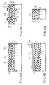
- the metal layer 121 may vanish, as shown in FIG. 75C.
- the intracell local interconnection cannot be formed.
- the intracell local interconnection 121-1 is hard to thin.
- the metal layer 121 Even if the metal layer 121 does not vanish, it is etched, as shown in FIG. 75B. For this reason, the thickness of the metal layer 121 varies.
- the etching amount of the metal layer 121 is not always uniform in, e.g., the chip or wafer. Hence, the thickness of the metal layer 121 varies in a wide range.
- the wide-ranging variation in thickness of the metal layer 121 causes, e.g., a variation in resistance value of the intracell local interconnection 121-1.
- the resistance value of the intracell local interconnection 121-1 varies, the resistance value of a resistor 200 between the bit line 113-1 and the cell transistor also varies, as shown in the equivalent circuit diagram shown in FIG. 76.
- Such a variation in resistance value may influence, e.g., the reliability related to a data read.
- a semiconductor integrated circuit device comprises: a cell transistor; a bit line provided above the cell transistor; an intracell local interconnection provided above the bit line and electrically connected to one of source and drain regions of the cell transistor; and a magnetoresistive element provided on the bit line and electrically connected to the bit line and the intracell local interconnection.
- a semiconductor integrated circuit device comprises: a bit line; a write word line provided above the bit line to cross the bit line; and a memory cell including a magnetoresistive element, the magnetoresistive element provided on the bit line and below the write word line.
- a method of manufacturing a semiconductor integrated circuit device comprises: forming a cell transistor on a semiconductor substrate; forming a first via connected to one of source and drain regions of the cell transistor and a source line connected to the other of the source and drain regions of the cell transistor; forming a second via connected to the first via and a bit line; forming a magnetoresistive element on the bit line; forming an intracell local interconnection connected to the magnetoresistive element and the second via; and forming a write word line above the intracell local interconnection.
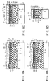
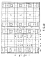
- FIG. 1 is a plan view showing the planar pattern of a magnetic random access memory according to a first embodiment of the present invention.
- FIG. 2A is a sectional view taken along a line A - A in FIG. 1.
- FIG. 2B is a sectional view taken along a line B - B in FIG. 1.
- FIG. 2C is a sectional view taken along a line C - C in FIG. 1.
- FIG. 2D is a sectional view of the substrate contact portion of a peripheral circuit.
- the magnetic random access memory has a memory cell including a magnetoresistive element.
- a memory cell including a magnetoresistive element a 1-magnetoresistive-element - 1-transistor memory cell including one magnetoresistive element and one cell transistor will be exemplified.
- the cell transistor is formed in the element region of, e.g., a p-type silicon substrate 1. The element region is defined by an element isolation region 2 formed on the substrate 1.
- the cell transistor has a gate electrode 4 and n-type source and drain regions 5.
- the gate electrode 4 functions as a read word line and extends in the first direction.
- a source line 9-1 and intracell via 9-2 are formed above the cell transistor.
- the source line 9-1 extends in the first direction, like the read word line, and is connected to one of the source and drain regions 5, e.g., the source region of the cell transistor through a first metal layer - substrate contact 7.
- the intracell via 9-2 is connected to the other of the source and drain regions 5, e.g., the drain region of the cell transistor through the first metal layer - substrate contact 7.
- a bit line 13-1 and intracell via 13-2 are formed above the source line 9-1 and the intracell via 9-2.
- These elements are formed from, e.g., a second metal layer.
- the intracell via 13-2 is connected to the intracell via 9-2 through a second metal layer - first metal layer contact 11.
- the bit line 13-1 extends in the second direction that crosses, e.g., is perpendicular to the read word line.
- a magnetoresistive element e.g., an Magnetic Tunnel Junction (MTJ) element 18 is formed on the bit line 13-1.
- the MTJ element 18 is a Tunneling Magneto Resistive (TMR) element.
- the MTJ element 18 includes a fixed-layer and memory-layer, which are formed from magnetic layers, e.g., ferromagnetic layers, and a tunnel barrier layer formed from an insulating nonmagnetic layer formed between the fixed-layer and the memory-layer. In the fixed-layer, the direction of spin is fixed. In the memory-layer, the direction of spin changes in accordance with the write magnetic field.
- One end of the MTJ element 18, e.g., the memory-layer is connected to the bit line 13-1.
- An intracell local interconnection 21-1 is formed on the MTJ element 18.
- the intracell local interconnection 21-1 is connected to the other end of the MTJ element 18, e.g., the fixed-layer and also connected to the intracell via 13-2 through an extra metal - second metal layer contact 20 (in the present invention, a conductive layer that forms the intracell local interconnection 21-1 is called an extra metal layer for the descriptive convenience).
- the MTJ element 18 is connected between the bit line 13-1 and the other of the source and drain regions 5, e.g., the drain region of the cell transistor.
- a write word line 24-1 is formed above the intracell local interconnection 21-1.
- the write word line 24-1 extends in the first direction, like, e.g., the read word line, to cross the bit line 13-1 on the upper side of the MTJ element 18.
- the write word line applies a magnetic field to the MTJ element 18.
- the easy axis of magnetization of the MTJ element 18 is set in the first direction in which the write word line 24-1 extends.
- the MTJ element 18 is formed under the intracell local interconnection 21-1.
- the intracell local interconnection 21-1 is not influenced when patterning the MTJ element 18.
- the intracell local interconnection 21-1 can be made thin, and the distance between the write word line 24-1 and the MTJ element 18 can be reduced.
- the MTJ element 18 can easily receive the magnetic field for the write word line 24-1 as compared to a typical magnetic random access memory having an MTJ element on an intracell local interconnection. Hence, data can easily be written in the MTJ element 18.
- the intracell local interconnection 21-1 is not influenced when patterning the MTJ element 18, any variation in thickness of the intracell local interconnection 21-1 can be suppressed. This also makes it possible to suppress a variation in resistance value between the bit line and the cell transistor. Hence, the reliability related to a data read can be improved.
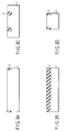
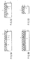
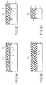
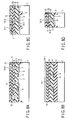
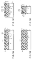
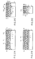
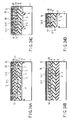
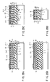
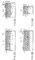
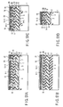
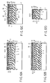
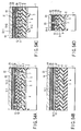
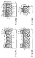
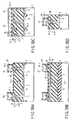
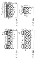
- FIGS. 3A to 15D are sectional views showing the method of manufacturing the magnetic random access memory according to the first embodiment of the present invention.
- FIGS. 3A, 4A, 5A, 6A, 7A, 8A, 9A, 10A, 11A, 12A, 13A, 14A, and 15A correspond to the section shown in FIG. 2A.
- FIGS. 3B, 4B, 5B, 6B, 7B, 8B, 9B, 10B, 11B, 12B, 13B, 14B, and 15B correspond to the section shown in FIG. 2B.
- FIGS. 3C, 4C, 5C, 6C, 7C, 8C, 9C, 10C, 11C, 12C, 13C, 14C, and 15C correspond to the section shown in FIG. 2C.
- FIGS. 3D, 4D, 5D, 6D, 7D, 8D, 9D, 10D, 11D, 12D, 13D, 14D, and 15D correspond to the section shown in FIG. 2D.
- a shallow trench corresponding to an element isolation region is formed in the p-type silicon substrate 1.
- the shallow trench is filled with an insulating material, e.g., SiO 2 to form an element isolation region (shallow trench isolation: STI).
- the substrate 1 corresponding to the element region defined by the element isolation region is thermally oxidized to form a gate insulating film (SiO 2 ) 3.
- Conductive polysilicon is deposited on the substrate 1 and on the element isolation region 2 to form a conductive polysilicon film.
- the conductive polysilicon film is patterned to form the gate electrode 4.
- An n-type impurity such as arsenic or phosphorus is ion-implanted into the substrate 1 using the gate electrode 4 and element isolation region 2 as a mask and diffused to form n-type source and drain regions 5.
- an insulating material e.g., SiO 2 is deposited on the structure shown in FIGS. 4A to 4D to form a first dielectric interlayer 6.
- a conductive material e.g., a metal such as tungsten to form the first metal layer - substrate contacts 7.
- an insulating material e.g., SiO 2 is deposited on the structure shown in FIGS. 5A to 5D to form a second dielectric interlayer 8.
- First metal layer interconnection trenches that reach the contacts 7 are formed in the second dielectric interlayer 8.
- the interconnection trenches are filled with a conductive material, e.g., a metal such as tungsten to form interconnection patterns of a first metal layer 9.
- a conductive material e.g., a metal such as tungsten to form interconnection patterns of a first metal layer 9.
- the source line 9-1, intracell via 9-2, and intra-peripheral-circuit via 9-3 are formed.
- an insulating material e.g., SiO 2 is deposited on the structure shown in FIGS. 6A to 6D to form a third dielectric interlayer 10.
- a conductive material e.g., a metal such as tungsten to form second metal layer - first metal layer contacts 11.
- an insulating material e.g., SiO 2 is deposited on the structure shown in FIGS. 7A to 7D to form a fourth dielectric interlayer 12.
- second layer metal interconnection trenches that reach the contacts 11 are formed in the fourth dielectric interlayer 12.
- the interconnection trenches are filled with a conductive material, e.g., a metal such as tungsten to form interconnection patterns of a second metal layer 13.
- a conductive material e.g., a metal such as tungsten to form interconnection patterns of a second metal layer 13.
- the bit line 13-1, the intracell via 13-2, and an intra-peripheral-circuit via 13-3 are formed.
- a ferromagnetic material e.g., CoFe or NiFe is sputtered on the structure shown in FIGS. 8A to 8D to form a ferromagnetic layer 14.
- an insulating material e.g., Alumina is deposited on the ferromagnetic layer 14 to form an insulating layer 15.
- a ferromagnetic material e.g., CoFe or NiFe is sputtered on the insulating layer 15 to form a ferromagnetic layer 16.
- a mask material is deposited on the ferromagnetic layer 16 to form a mask layer 17.
- the mask layer 17 is patterned into a shape corresponding to the layout pattern of the MTJ element.
- the ferromagnetic layer 16, insulating layer 15, and ferromagnetic layer 14 are sequentially etched using the mask layer 17 as a mask.
- the MTJ element 18 having, e.g., a three-layered structure including the ferromagnetic layer 14, insulating layer 15, and ferromagnetic layer 16 is formed.
- the ferromagnetic layer 14 functions as a memory-layer in which the direction of spin changes in accordance with the write magnetic field.
- the insulating layer 15 functions as a tunnel barrier.
- the ferromagnetic layer 16 functions as a fixed-layer in which the direction of spin is fixed. Note that the MTJ element 18 is not limited to the above three-layered structure.
- an insulating material e.g., SiO 2 is deposited on the structure shown in FIGS. 10A to 10D to form a fifth dielectric interlayer 19.
- the fifth dielectric interlayer 19 is subjected to, e.g., chemical mechanical polishing (CMP) to expose the MTJ element 18.
- CMP chemical mechanical polishing
- an opening that reaches the intracell via 13-2 is formed in the fifth dielectric interlayer 19.
- the opening is filled with a conductive material, e.g., a metal such as tungsten to form an extra metal - second metal layer contact 20.
- a conductive material e.g., a metal such as tungsten is deposited on the structure shown in FIGS. 11A to 11D to form an extra metal layer 21.
- the thickness of the extra metal layer 21, i.e., the thickness of the extra metal layer in the typical magnetic random access memory can be made small.
- the extra metal layer 21 is patterned to form the intracell local interconnection 21-1.
- an insulating material e.g., SiO 2 is deposited on the structure shown in FIGS. 13A to 13D to form a sixth dielectric interlayer 22.
- An opening that reaches the intra-peripheral-circuit via 13-3 is formed in the sixth dielectric interlayer 22 and fifth dielectric interlayer 19.
- the opening is filled with a conductive material, e.g., a metal such as tungsten to form a third metal layer - second metal layer contact 23.
- a conductive material such as AlCu or Cu is deposited on the structure shown in FIGS. 14A to 14D to form a third metal layer 24.
- a conductive material such as AlCu or Cu is deposited on the structure shown in FIGS. 14A to 14D to form a third metal layer 24.
- AlCu or Cu is used for the third metal layer 24, it is generally sandwiched between barrier metal layers.
- barrier metal layers may be formed under and on the third metal layer 24.
- the material of the barrier metal layer are Ti, TiN, Ta, TaN, and W.
- the third metal layer 24 is patterned to form the write word line 24-1 and an intra-peripheral-circuit interconnection 24-2.
- the magnetic random access memory according to the first embodiment can be formed.
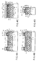
- FIG. 16 is a plan view showing the planar pattern of a magnetic random access memory according to a second embodiment of the present invention.
- FIG. 17A is a sectional view taken along a line A - A in FIG. 16.
- FIG. 17B is a sectional view taken along a line B - B in FIG. 16.
- FIG. 17C is a sectional view taken along a line C - C in FIG. 16.
- FIG. 17D is a sectional view of the substrate contact portion of a peripheral circuit.
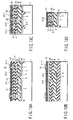
- the magnetic random access memory of the second embodiment is different from the first embodiment in that a yoke layer 28 that covers the upper and side surfaces of a write word line 24-1 and the side surface of an MTJ element 18 to confine the magnetic field from the write word line 24-1 is formed.
- the yoke layer 28 of this embodiment is made of, e.g., a conductive magnetic material. Since the yoke layer 28 of this embodiment is formed from a conductive magnetic material, it is separated for each write word line 24-1. Additionally, in this embodiment, a yoke layer 26 that covers the bottom and side surfaces of a bit line 13-1 is formed.
- the magnetic random access memory according to the second embodiment has the yoke layer 28 that covers the upper and side surfaces of the write word line 24-1 and the side surface of the MTJ element 18. For this reason, as compared to a structure without the yoke layer 28, the magnetic field from the write word line 24-1 can be efficiently applied to the MTJ element 18.
- an adjacent unselected MTJ element 18 is hard to be influenced by the magnetic field from the selected write word line 24-1. For this reason, the reliability related to, e.g., a data read can be improved.
- the magnetic field from the bit line 13-1 can be efficiently applied to the MTJ element in a data write mode.
- the yoke layer 26 is not in contact with the yoke layer 28. Since the yoke layer 26 is not in contact with the yoke layer 28, for example, any interference between the magnetic field from the yoke layer 26 and that from the yoke layer 28 can advantageously be suppressed.
- a first method of manufacturing the magnetic random access memory according to the second embodiment of the present invention will be described next.
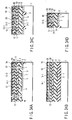
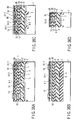
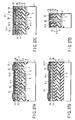
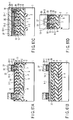
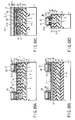
- FIGS. 18A to 31D are sectional views showing the first method of manufacturing the magnetic random access memory according to the second embodiment of the present invention.
- FIGS. 18A, 19A, 20A, 21A, 22A, 23A, 24A, 25A, 26A, 27A, 28A, 29A, 30A, and 31A correspond to the section shown in FIG. 17A.
- FIGS. 18B, 19B, 20B, 21B, 22B, 23B, 24B, 25B, 26B, 27B, 28B, 29B, 30B, and 31B correspond to the section shown in FIG. 17B.
- FIGS. 18C, 19C, 20C, 21C, 22C, 23C, 24C, 25C, 26C, 27C, 28C, 29C, 30C, and 31C correspond to the section shown in FIG. 17C.
- FIGS. 18D, 19D, 20D, 21D, 22D, 23D, 24D, 25D, 26D, 27D, 28D, 29D, 30D, and 31D correspond to the section shown in FIG. 17D.
- FIGS. 18A to 18D is obtained by the manufacturing method described with reference to FIGS. 3A to 7D.
- an insulating material e.g., SiO 2 is deposited on the structure shown in FIGS. 18A to 18D to form a fourth dielectric interlayer 12.
- Second metal layer interconnection trenches 25 that reach contacts 11 are formed in the fourth dielectric interlayer 12.
- a bit line trench 25-1, intracell via trench 25-2, and intra-peripheral-circuit via trench 25-3 are formed.
- a conductive or insulating yoke material is deposited on the structure shown in FIGS. 19A to 19D to form the yoke layer 26.
- the conductive yoke layer 26 is exemplified.
- a conductive yoke material for example, an Ni-Fe alloy, Co-Fe-Ni alloy, Co-(Zr, Hf, Nb, Ta, Ti) film, or (Co, Fe, Ni)-(Si, B)-(P, Al, Mo, Nb, Mn)-based amorphous material can be used.
- insulating yoke material for example, insulating ferrite, (Fe, Co)-(B, Si, Hf, Zr, Sm, Ta, Al)-(F, O, N)-based metal-nonmetal nanogranular film can be used.
- a conductive material e.g., a metal such as tungsten is deposited on the conductive yoke layer 26 to form a second metal layer 13.
- the second metal layer 13 and conductive yoke layer 26 are subjected to, e.g., chemical mechanical polishing (CMP) to fill the bit line trench 25-1, intracell via trench 25-2, and intra-peripheral-circuit via trench 25-3 with the second metal layer and conductive yoke material.
- CMP chemical mechanical polishing
- a ferromagnetic material is sputtered on the structure shown in FIGS. 21A to 21D to form a ferromagnetic layer 14.
- an insulating material is deposited on the ferromagnetic layer 14 to form an insulating layer 15.
- a ferromagnetic material is sputtered on the insulating layer 15 to form a ferromagnetic layer 16.
- a mask material is deposited on the ferromagnetic layer 16 to form a mask layer 17.
- the mask layer 17 is patterned into a shape corresponding to the layout pattern of the MTJ element.
- the ferromagnetic layer 16, insulating layer 15, and ferromagnetic layer 14 are sequentially etched using the mask layer 17 as a mask.
- the MTJ element 18 having, e.g., a three-layered structure including the ferromagnetic layer 14, insulating layer 15, and ferromagnetic layer 16 is formed.
- the ferromagnetic layer 14 functions as a memory-layer in which the direction of spin changes in accordance with the write magnetic field.
- the insulating layer 15 functions as a tunnel barrier.
- the ferromagnetic layer 16 functions as a fixed-layer in which the direction of spin is fixed.
- an insulating material e.g., SiO 2 is deposited on the structure shown in FIGS. 23A to 23D to form a fifth dielectric interlayer 19.
- the fifth dielectric interlayer 19 is subjected to, e.g., chemical mechanical polishing (CMP) to expose the MTJ element 18.
- CMP chemical mechanical polishing
- an opening that reaches the intracell via 13-2 is formed in the fifth dielectric interlayer 19.
- the opening is filled with a conductive material, e.g., a metal such as tungsten to form an extra metal - second metal layer contact 20.
- a conductive material e.g., a metal such as tungsten is deposited on the structure shown in FIGS. 24A to 24D to form an extra metal layer 21.
- the extra metal layer 21 is patterned to form an intracell local interconnection 21-1.
- an insulating material e.g., SiO 2 is deposited on the structure shown in FIGS. 26A to 26D to form a sixth dielectric interlayer 22.
- An opening that reaches the intra-peripheral-circuit via 13-3 is formed in the sixth dielectric interlayer 22 and fifth dielectric interlayer 19.
- the opening is filled with a conductive material, e.g., a metal such as tungsten to form a third metal layer - second metal layer contact 23.
- a conductive material e.g., AlCu or Cu is deposited on the structure shown in FIGS. 27A to 27D to form a third metal layer 24.
- a conductive yoke material is deposited on the third metal layer 24 to form a conductive yoke layer 27.
- a material of the conductive yoke layer 27 for example, an Ni-Fe alloy, Co-Fe-Ni alloy, Co-(Zr, Hf, Nb, Ta, Ti) film, or (Co, Fe, Ni)-(Si, B)-(P, Al, Mo, Nb, Mn)-based amorphous material can be used.
- the conductive yoke layer 27, third metal layer 24, and sixth dielectric interlayer 22 are etched using a mask material (not shown) corresponding to the write word line pattern and intra-peripheral-circuit interconnection pattern as a mask.
- the fifth dielectric interlayer 19 is etched halfway. With this process, a write word line 24-1 and intra-peripheral-circuit interconnection 24-2 are formed.
- the reason why the fifth dielectric interlayer 19 is etched halfway is that the yoke layer 28 to be formed later need be brought close to, e.g., the bit line 13-1 as much as possible.
- the reason why the fifth dielectric interlayer is not etched until the bit line 13-1 is exposed is that the yoke layer 26 need be prevented from coming into contact with the yoke layer 28 to be formed later.
- a conductive yoke material is deposited on the structure shown in FIGS. 29A to 29D to form the conductive yoke layer 28.
- a material of the conductive yoke layer 28 for example, an Ni-Fe alloy, Co-Fe-Ni alloy, Co-(Zr, Hf, Nb, Ta, Ti) film, or (Co, Fe, Ni)-(Si, B)-(P, Al, Mo, Nb, Mn)-based amorphous material can be used, like the conductive yoke layer 27.
- the conductive yoke layer 28 is anisotropically etched using anisotropic etching, e.g., reactive ion etching (RIE) to leave the conductive yoke layer 28 on the side surfaces of the conductive yoke layer 27, write word line 24-1 or intra-peripheral-circuit interconnection 24-2, sixth dielectric interlayer 22, and fifth dielectric interlayer 19.
- anisotropic etching e.g., reactive ion etching (RIE)
- the magnetic random access memory according to the second embodiment can be formed.
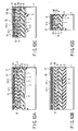
- FIGS. 32A to 41D are sectional views showing the second method of manufacturing the magnetic random access memory according to the second embodiment of the present invention.
- FIGS. 32A, 33A, 34A, 35A, 36A, 37A, 38A, 39A, 40A, and 41A correspond to the section shown in FIG. 17A.
- FIGS. 32B, 33B, 34B, 35B, 36B, 37B, 38B, 39B, 40B, and 41B correspond to the section shown in FIG. 17B.
- FIGS. 32C, 33C, 34C, 35C, 36C, 37C, 38C, 39C, 40C, and 41C correspond to the section shown in FIG. 17C.
- FIGS. 32D, 33D, 34D, 35D, 36D, 37D, 38D, 39D, 40D, and 41D correspond to the section shown in FIG. 17D.
- FIGS. 32A to 32D is obtained by the manufacturing method described with reference to FIGS. 3A to 7D and FIGS. 19A to 23D.
- an insulating material e.g., SiN is deposited on the structure shown in FIGS. 32A to 32D to form a stopper layer 29.
- an insulating material e.g., SiO 2 is deposited on the stopper layer 29 to form the fifth dielectric interlayer 19.
- An example of the material of the stopper layer 29 is SiN. However, any other material that can ensure an etching selectivity ratio with respect to the fifth dielectric interlayer 19 can be used.
- the fifth dielectric interlayer 19 and stopper layer 29 are subjected to, e.g., chemical mechanical polishing (CMP) to expose the MTJ element 18.
- CMP chemical mechanical polishing
- an opening that reaches the intracell via 13-2 is formed in the fifth dielectric interlayer 19 and stopper layer 29.
- the opening is filled with a conductive material, e.g., a metal such as tungsten to form the extra metal - second metal layer contact 20.
- a conductive material e.g., a metal such as tungsten is deposited on the structure shown in FIGS. 34A to 34D to form the extra metal layer 21.
- the extra metal layer 21 is patterned to form the intracell local interconnection 21-1.
- an insulating material e.g., SiO 2 is deposited on the structure shown in FIGS. 36A to 36D to form a sixth dielectric interlayer 22.
- An opening that reaches the intra-peripheral-circuit via 13-3 is formed in the sixth dielectric interlayer 22 and fifth dielectric interlayer 19.
- the opening is filled with a conductive material, e.g., a metal such as tungsten to form the third metal layer - second metal layer contact 23.
- a conductive material e.g., AlCu or Cu is deposited on the structure shown in FIGS. 37A to 37D to form the third metal layer 24.
- a conductive yoke material is deposited on the third metal layer 24 to form the conductive yoke layer 27.
- the conductive yoke layer 27, third metal layer 24, sixth dielectric interlayer 22, and fifth dielectric interlayer 19 are etched using a mask material (not shown) corresponding to the write word line pattern and intra-peripheral-circuit interconnection pattern as a mask, e.g., until the stopper layer 29 is exposed. With this process, the write word line 24-1 and intra-peripheral-circuit interconnection 24-2 are formed.
- a conductive yoke material is deposited on the structure shown in FIGS. 39A to 39D to form the conductive yoke layer 28.
- the conductive yoke layer 28 is anisotropically etched using anisotropic etching, e.g., reactive ion etching (RIE) to leave the conductive yoke layer 28 on the side surfaces of the conductive yoke layer 27, write word line 24-1 or intra-peripheral-circuit interconnection 24-2, sixth dielectric interlayer 22, and fifth dielectric interlayer 19.
- anisotropic etching e.g., reactive ion etching (RIE)
- the magnetic random access memory according to the second embodiment can be formed.
- a third method of manufacturing the magnetic random access memory according to the second embodiment of the present invention will be described next.
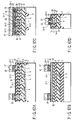
- FIGS. 42A to 47D are sectional views showing the third method of manufacturing the magnetic random access memory according to the second embodiment of the present invention.
- FIGS. 42A, 43A, 44A, 45A, 46A, and 47A correspond to the section shown in FIG. 17A.
- FIGS. 42B, 43B, 44B, 45B, 46B, and 47B correspond to the section shown in FIG. 17B.
- FIGS. 42C, 43C, 44C, 45C, 46C, and 47C correspond to the section shown in FIG. 17C.
- FIGS. 42D, 43D, 44D, 45D, 46D, and 47D correspond to the section shown in FIG. 17D.
- FIGS. 42A to 42D is obtained by the manufacturing method described with reference to FIGS. 3A to 7D and FIGS. 19A to 27D.
- an insulating material e.g., SiO 2 is deposited on the structure shown in FIGS. 42A to 42D to form a seventh dielectric interlayer 30.
- Third layer metal interconnection trenches 31 are formed in the seventh dielectric interlayer 30. With this process, a write word line trench 31-1 and intra-peripheral-circuit interconnection trench 31-2 are formed.
- a conductive material e.g., AlCu or Cu is deposited on the structure shown in FIGS. 42A to 42D to form the third metal layer 24.
- the third metal layer 24 is, e.g., etched back to bury the third metal layer 24 halfway in the write word line trench 31-1 and intra-peripheral-circuit interconnection trench 31-2.
- a conductive yoke material is deposited on the third metal layer 24 and seventh dielectric interlayer 30 to form the conductive yoke layer 27.
- the conductive yoke layer 27 is subjected to, e.g., chemical mechanical polishing (CMP) to bury it in the write word line trench 31-1 and intra-peripheral-circuit interconnection trench 31-2.
- CMP chemical mechanical polishing
- the conductive yoke layer 27, third metal layer 24, seventh dielectric interlayer 30, and sixth dielectric interlayer 22 are etched using a mask material (not shown) corresponding to the write word line pattern and intra-peripheral-circuit interconnection pattern as a mask.
- the fifth dielectric interlayer 19 is etched halfway. With this process, the write word line 24-1 and intra-peripheral-circuit interconnection 24-2 are formed.
- the seventh dielectric interlayer 30 is, e.g., wet-etched to remove the seventh dielectric interlayer 30 that is present on the side surface of the conductive yoke layer 27. With this process, a portion 32 where the side surface of the conductive yoke layer 27 is exposed is obtained. This process is executed as needed.
- a conductive yoke material is deposited on the structure shown in FIGS. 46A to 46D to form the conductive yoke layer 28.
- the conductive yoke layer 28 is anisotropically etched using anisotropic etching, e.g., reactive ion etching (RIE) to leave the conductive yoke layer 28 on the side surfaces of the conductive yoke layer 27, write word line 24-1 or intra-peripheral-circuit interconnection 24-2, seventh dielectric interlayer 30, sixth dielectric interlayer 22, and fifth dielectric interlayer 19.
- anisotropic etching e.g., reactive ion etching (RIE)
- the magnetic random access memory according to the second embodiment can be formed.
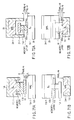
- FIGS. 48A, 48B, 48C, and 48D are sectional views showing the modification to the magnetic random access memory according to the second embodiment of the present invention.
- FIG. 48A corresponds to the section shown in FIG. 17A.
- FIG. 48B corresponds to the section shown in FIG. 17B.
- FIG. 48C corresponds to the section shown in FIG. 17C.
- FIG. 48D corresponds to the section shown in FIG. 17D.
- the conductive yoke layer 28 may be formed to cover the side surfaces of the write word line 24-1 and MTJ element 18.
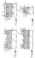
- FIG. 49 is a plan view showing the planar pattern of a magnetic random access memory according to the third embodiment of the present invention.
- FIG. 50A is a sectional view taken along a line A - A in FIG. 49.
- FIG. 50B is a sectional view taken along a line B - B in FIG. 49.
- FIG. 50C is a sectional view taken along a line C - C in FIG. 49.
- FIG. 50D is a sectional view of the substrate contact portion of a peripheral circuit.
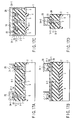
- the magnetic random access memory of the third embodiment is different from the second embodiment in that a yoke layer 34 is made of an insulating material.
- an intracell local interconnection 21-1 may be in contact with the yoke layer 34. This is advantageous in micropatterning a memory cell as compared to a memory having a conductive yoke layer. This is because, for example, in forming a write word line 24-1, no mask alignment margin for, e.g., the intracell local interconnection 21-1 need be taken into consideration.
- the intracell local interconnection 21-1 can be in contact with the yoke layer 34, the intracell local interconnection 21-1 can be widened.
- the width of the intracell local interconnection 21-1 can be equalized with that of the write word line 24-1.
- the resistance value of the intracell local interconnection 21-1 can be made small.
- FIGS. 51A to 56D are sectional views showing the method of manufacturing the magnetic random access memory according to the third embodiment of the present invention.
- FIGS. 51A, 52A, 53A, 54A, 55A, and 56A correspond to the section shown in FIG. 50A.
- FIGS. 51B, 52B, 53B, 54B, 55B, and 56B correspond to the section shown in FIG. 50B.
- FIGS. 51C, 52C, 53C, 54C, 55C, and 56C correspond to the section shown in FIG. 50C.
- FIGS. 51D, 52D, 53D, 54D, 55D, and 56D correspond to the section shown in FIG. 50D.
- FIGS. 51A to 51D is obtained by the manufacturing method described with reference to FIGS. 3A to 7D and FIGS. 19A to 25D.
- an extra metal layer 21 is etched to form a slit 33 in the extra metal layer 21.
- the slit 33 extends in the same direction as that of, e.g., a bit line 13-1 and serves as an isolation region for sequentially isolating the intracell local interconnection 21-1 to be formed later along the direction in which, e.g., a read word line 4 extends.
- an insulating material e.g., SiO 2 is deposited on the structure shown in FIGS. 52A to 52D to form a sixth dielectric interlayer 22.
- An opening that reaches an intra-peripheral-circuit via 13-3 is formed in the sixth dielectric interlayer 22 and fifth dielectric interlayer 19.
- the opening is filled with a conductive material, e.g., a metal such as tungsten to form a third metal layer - second metal layer contact 23.
- a conductive material e.g., AlCu or Cu is deposited on the structure shown in FIGS. 53A to 53D to form a third metal layer 24.
- the third metal layer 24, sixth dielectric interlayer 22, and extra metal layer 21 are etched using a mask material (not shown) corresponding to the write word line pattern and intra-peripheral-circuit interconnection pattern as a mask.
- the fifth dielectric interlayer 19 is etched halfway. With this process, the write word line 24-1, the intra-peripheral-circuit interconnection 24-2, and the intracell local interconnection 21-1 are formed.
- an insulating yoke material is deposited on the structure shown in FIGS. 55A to 55D to form the insulating yoke layer 34.
- a material of the insulating yoke layer 34 for example, an insulating ferrite, (Fe, Co)-(B, Si, Hf, Zr, Sm, Ta, Al)-(F, O, N)-based metal-nonmetal nanogranular film can be used.
- the magnetic random access memory according to the third embodiment can be formed.
- FIGS. 57A, 57B, 57C, and 57D are sectional views showing the first modification to the magnetic random access memory according to the third embodiment of the present invention.
- FIG. 57A corresponds to the section shown in FIG. 50A.
- FIG. 57B corresponds to the section shown in FIG. 50B.
- FIG. 57C corresponds to the section shown in FIG. 50C.
- FIG. 57D corresponds to the section shown in FIG. 50D.
- the insulating yoke layer 34 may be formed to cover the side surfaces of the write word line 24-1 and MTJ element 18.
- FIGS. 58A, 58B, 58C, and 58D are sectional views showing the second modification to the magnetic random access memory according to the third embodiment of the present invention.
- FIG. 58A corresponds to the section shown in FIG. 50A.
- FIG. 58B corresponds to the section shown in FIG. 50B.
- FIG. 58C corresponds to the section shown in FIG. 50C.
- FIG. 58D corresponds to the section shown in FIG. 50D.
- the side surfaces of the write word line 24-1 and MTJ element 18 may be covered with the insulating yoke layer 34, and the upper surface of the write word line 24-1 may be covered with a conductive yoke layer 27.
- FIGS. 59A to 62D are sectional views showing a method of manufacturing a magnetic random access memory according to a fourth embodiment of the present invention.
- FIGS. 59A, 60A, 61A, and 62A correspond to the section shown in FIG. 17A.
- FIGS. 59B, 60B, 61B, and 62B correspond to the section shown in FIG. 17B.
- FIGS. 59C, 60C, 61C, and 62C correspond to the section shown in FIG. 17C.
- FIGS. 59D, 60D, 61D, and 62D correspond to the section shown in FIG. 17D.
- FIGS. 59A to 59D is obtained by the manufacturing method described with reference to FIGS. 3A to 7D and FIGS. 19A to 28D.
- a conductive yoke layer 27 and third metal layer 24 are etched using a mask material (not shown) corresponding to the write word line pattern and intra-peripheral-circuit interconnection pattern as a mask. With this process, a write word line 24-1 and intra-peripheral-circuit interconnection 24-2 are formed.
- a mask layer 35 of, e.g., a photoresist is formed to cover the peripheral circuit portion.
- a sixth dielectric interlayer 22 and fifth dielectric interlayer 19 are etched halfway using the mask layer 35 and write word line 24-1, and particularly, the yoke layer 27 in this embodiment as a mask. With this process, a recess used to form the yoke layer is formed only, e.g., at the memory cell portion where memory cells are integrated. After that, the mask layer 35 is removed in this embodiment.
- a conductive yoke material is deposited on the exposed surface of the fifth dielectric interlayer 19, on the exposed surface of the write word line 24-1, on the exposed surface of the yoke layer 27, and on the sixth dielectric interlayer 22 to form a conductive yoke layer 28. Then, the conductive yoke layer 28 is left on the side surfaces of the conductive yoke layer 27, write word line 24-1 or intra-peripheral-circuit interconnection 24-2, sixth dielectric interlayer 22, and fifth dielectric interlayer 19.
- the recess used to form the yoke layer 28 can be formed only, e.g., at the memory cell array portion so that, e.g., the peripheral circuit portion can have satisfactory planarity.
- the interconnection process using the fourth metal layer, fifth metal layer,... above the third metal layer can easily be executed in, e.g., the peripheral circuit portion.
- FIGS. 63A to 69D are sectional views showing a method of manufacturing a magnetic random access memory according to a fifth embodiment of the present invention.
- FIGS. 63A, 64A, 65A, 66A, 67A, 68A, and 69A correspond to the section shown in FIG. 17A.
- FIGS. 63B, 64B, 65B, 66B, 67B, 68B, and 69B correspond to the section shown in FIG. 17B.
- FIGS. 63C, 64C, 65C, 66C, 67C, 68C, and 69C correspond to the section shown in FIG. 17C.
- FIGS. 63D, 64D, 65D, 66D, 67D, 68D, and 69D correspond to the section shown in FIG. 17D.
- FIGS. 63A to 63D is obtained by the manufacturing method described with reference to FIGS. 3A to 7D and FIGS. 19A to 25D.
- an extra metal layer 21 is etched to form a slit 33 in the extra metal layer 21.
- the slit 33 is similar to the slit 33 shown in FIGS. 52A to 52D.
- the slit 33 extends in the same direction as that of, e.g., a bit line 13-1 and serves as an isolation region for sequentially isolating the intracell local interconnection 21-1 to be formed later along the direction in which, e.g., a read word line 4 extends.
- an insulating material e.g., SiO 2 is deposited on the structure shown in FIGS. 64A to 64D to form a sixth dielectric interlayer 22.
- An opening that reaches an intra-peripheral-circuit via 13-3 is formed in the sixth dielectric interlayer 22 and fifth dielectric interlayer 19.
- the opening is filled with a conductive material, e.g., a metal such as tungsten to form a third metal layer - second metal layer contact 23.
- a conductive material e.g., AlCu or Cu is deposited on the structure shown in FIGS. 65A to 65D to form a third metal layer 24.
- a conductive yoke material is deposited on the third metal layer 24 to form a conductive yoke layer 27.
- a material of the conductive yoke layer 27 for example, an Ni-Fe alloy, Co-Fe-Ni alloy, Co-(Zr, Hf, Nb, Ta, Ti) film, or (Co, Fe, Ni)-(Si, B)-(P, Al, Mo, Nb, Mn)-based amorphous material can be used.
- the conductive yoke layer 27, third metal layer 24, sixth dielectric interlayer 22, and extra metal layer 21 are etched using a mask material (not shown) corresponding to the write word line pattern and intra-peripheral-circuit interconnection pattern as a mask.
- the fifth dielectric interlayer 19 is etched halfway. With this process, the write word line 24-1, the intra-peripheral-circuit interconnection 24-2, and the intracell local interconnection 21-1 are formed.
- an insulating material e.g., SiO 2 is deposited on the structure shown in FIGS. 67A to 67D to form an insulation layer 36.
- the insulation layer 36 is anisotropically etched using anisotropic etching, e.g., reactive ion etching (RIE) to leave the insulation layer 36 on the side surfaces of the write word line 24-1, intra-peripheral-circuit interconnection 24-2, sixth dielectric interlayer 22, intracell local interconnection 21-1, and fifth dielectric interlayer 19. A portion of the side surface of the conductive yoke layer 27 is exposed.
- anisotropic etching e.g., reactive ion etching
- a conductive yoke material is deposited on the structure shown in FIGS. 68A to 68D to form the conductive yoke layer 28.
- a material of the conductive yoke layer 28 for example, an Ni-Fe alloy, Co-Fe-Ni alloy, Co-(Zr, Hf, Nb, Ta, Ti) film, or (Co, Fe, Ni)-(Si, B)-(P, Al, Mo, Nb, Mn)-based amorphous material can be used, like the conductive yoke layer 27.
- the conductive yoke layer 28 is anisotropically etched using anisotropic etching, e.g., reactive ion etching (RIE) to leave the conductive yoke layer 28 on the side surfaces of the conductive yoke layer 27 and the insulation layer 36.
- anisotropic etching e.g., reactive ion etching (RIE)
- the intracell local interconnection 21-1 can be patterned and formed simultaneously with the write word line 24-1. For this reason, the intracell local interconnection 21-1 can have the same width as that of the write word line 24-1, and the resistance value of the intracell local interconnection 21-1 can advantageously be decreased.
- an MTJ element can be used as a magnetoresistive element.
- MTJ element Several examples of an MTJ element will be described below.
- FIG. 70A is a sectional view showing the first example of an MTJ element.
- an antiferromagnetic layer 51, ferromagnetic layer 52, tunnel barrier layer 53, ferromagnetic layer 54, and protective layer 55 are sequentially formed on an underlying layer 50.
- the ferromagnetic layer 52 functions as a fixed-layer in which the direction of spin is fixed.
- the ferromagnetic layer 54 functions as a memory-layer in which the direction of spin can be changed.
- the antiferromagnetic layer 51 fixes the direction of spin in the ferromagnetic layer 52.
- the direction of spin in the ferromagnetic layer 52 which functions as a fixed-layer, as in this example, may be fixed using, e.g., the antiferromagnetic layer 51.
- the underlying layer 50 makes it possible to easily form, e.g., the ferromagnetic layer or antiferromagnetic layer or protect the layer and is formed as needed.
- the protective layer 55 protects, e.g., the ferromagnetic layer or antiferromagnetic layer.
- the protective layer 55 is also formed, as needed, like the underlying layer 50. Matters about the underlying layer 50 and protective layer 55 also apply to the second to fourth examples to be described below.
- Examples of the material of the ferromagnetic layer 52 or 54 are as follows. Fe, Co, Ni, or an alloy thereof Magnetite with high spin polarization ratio An oxide such as CrO 2 or RXMnO 3 -y (R: rare earth. X : Ca, Ba, Sr) Heusler alloy such as NiMnSb or PtMnSb
- the ferromagnetic material 52 or 54 may contain a nonmagnetic element within a range in which the ferromagnetism is not lost.
- nonmagnetic element examples include Ag, Cu, Au, Al, Mg, Si, Bi, Ta, B, C, O, N, Pd, Pt, Zr, Ir, W, Mo, and Nb
- the ferromagnetic layer 52 or 54 has such a thickness that the ferromagnetic layer 52 or 54 does not become super-paramagnetic. More specifically, the ferromagnetic layer 52 or 54 is formed to a thickness of 0.4 nm or more. The thickness of the ferromagnetic layer 52 or 54 has no particular upper limit. However, the thickness of the ferromagnetic layer 52 or 54 is preferably, e.g., 100 nm or less from the viewpoint of formation of the MTJ element.
- Examples of the material of the antiferromagnetic layer 51 are as follows. Fe-Mn, Pt-Mn, Pt-Cr-Mn, Ni-Mn, Ir-Mn, NiO, and Fe 2 O 3
- Examples of the material of the tunnel barrier layer 53 are as follows. Al 2 O 3 , SiO 2 , MgO, AlN, Bi 2 O 3 , MgF 2 , CaF 2 , SrTiO 2 , and AlLaO 3
- the material of the tunnel barrier layer 53 may contain at least one of oxygen, nitrogen, and fluorine within a range in which the tunnel barrier layer 53 does not lose, e.g., the insulting properties.
- at least one of oxygen, nitrogen, and fluorine may be omitted within a range in which the tunnel barrier layer 53 does not lose, e.g., the insulting properties.
- the thickness of the tunnel barrier layer 53 is preferably as much as small but is not particularly limited.
- the thickness of the tunnel barrier layer 53 is set to 10 nm or less from the viewpoint of formation of the MTJ element.
- FIG. 70B is a sectional view showing the second example of an MTJ element.
- the MTJ element of the second example is an MTJ element called a double-junction type.
- an antiferromagnetic layer 51-1, ferromagnetic layer 52-1, tunnel barrier layer 53-1, ferromagnetic layer 54, tunnel barrier layer 53-2, ferromagnetic layer 52-2, antiferromagnetic layer 51-2, and protective layer 55 are sequentially formed on an underlying layer 50.
- the ferromagnetic layers 52-1 and 52-2 function as fixed-layers.
- the ferromagnetic layer 54 functions as a memory-layer.
- the antiferromagnetic layer 51-1 fixes the direction of spin in the ferromagnetic layer 52-1.
- the antiferromagnetic layer 51-2 fixes the direction of spin in the ferromagnetic layer 52-2.
- the double-junction-type MTJ element as in this example can increase the ratio of a resistance value in a low resistance mode to that in a high resistance mode, i.e., so-called MR ratio (Magneto-Resistance ratio) as compared to, e.g., the MTJ element (single-junction-type) shown in FIG. 70A.
- MR ratio Magnetic-Resistance ratio
- Examples of the materials of the antiferromagnetic layers 51-1 and 51-2, ferromagnetic layers 52-1, 52-2, and 54, and tunnel barrier layers 53-1 and 53-2 are the same as described in the first example.
- Examples of the thicknesses of the ferromagnetic layers 52-1, 52-2, and 54 are the same as described in the first example.
- Examples of the materials and thicknesses of the tunnel barrier layers 53-1 and 53-2 are the same as described in the first example.
- FIG. 70C is a sectional view showing the third example of an MTJ element.
- each of ferromagnetic layers 52 and 54 in the MTJ element of the first example has a stack structure of a ferromagnetic layer and nonmagnetic layer.
- An example of the stack structure is a three-layered structure of ferromagnetic layer/nonmagnetic layer/ferromagnetic layer.
- the ferromagnetic layer 52 has a three-layered structure of ferromagnetic layer 61/nonmagnetic layer 62/ferromagnetic layer 63.
- the ferromagnetic layer 54 has a three-layered structure of ferromagnetic layer 64/nonmagnetic layer 65/ferromagnetic layer 66.
- Examples of the material of the ferromagnetic layers 61, 63, 64, and 66 are the same as described in the first example.
- Examples of the material of the nonmagnetic layers 62 and 65 are as follows. Ru, Ir,
- ferromagnetic layer/nonmagnetic layer/ferromagnetic layer Detailed examples of the three-layered structure of ferromagnetic layer/nonmagnetic layer/ferromagnetic layer are as follows. Co/Ru/Co, Co/Ir/Co Co-Fe/Ru/Co-Fe, Co-Fe/Ir/Co-Fe
- the ferromagnetic layer 52 that functions as a fixed-layer has a stack structure, e.g., a three-layered structure of ferromagnetic layer 61/nonmagnetic layer 62/ferromagnetic layer 63, antiferromagnetic bond is preferably generated between the ferromagnetic layer 61 and the ferromagnetic layer 63 through the nonmagnetic layer 62.
- an antiferromagnetic layer 51 is formed in contact with the three-layered structure. With this structure, the direction of spin in the ferromagnetic layer 52 and, more particularly, the ferromagnetic layer 63 functioning as a fixed-layer can be more firmly fixed.
- the ferromagnetic layer 52 and, more particularly, the ferromagnetic layer 63 is hardly affected by the current field. Hence, any unexpected reversal of the direction of spin in the ferromagnetic layer 52 that function as a fixed-layer can be suppressed.
- the ferromagnetic layer 54 that functions as a memory-layer has a stack structure, e.g., a three-layered structure of ferromagnetic layer 64/nonmagnetic layer 65/ferromagnetic layer 66, antiferromagnetic bond is preferably generated between the ferromagnetic layer 64 and the ferromagnetic layer 66 through the nonmagnetic layer 65.
- the magnetic flux closes in the three-layered structure, any increase in switching field due to, e.g., the magnetic pole can be suppressed.
- any increase in power consumption due to a current field by a diamagnetic field can advantageously be suppressed.
- the ferromagnetic layer 54 that functions as a memory-layer may have a stack structure of a soft ferromagnetic layer and a ferromagnetic layer.
- a soft ferromagnetic layer means a layer whose direction of spin is more readily reversed as compared to, e.g., a ferromagnetic layer.
- the soft ferromagnetic layer 54 has a stack structure of a soft ferromagnetic layer and a ferromagnetic layer
- the soft ferromagnetic layer is arranged on a side close to a current field line, e.g., a bit line.
- This stack structure may also include a nonmagnetic layer.
- a nonmagnetic layer For example, as in this example, when a three-layered structure of ferromagnetic layer 64/nonmagnetic layer 65/ferromagnetic layer 66 is formed, e.g., the ferromagnetic layer 66 may be formed as a soft ferromagnetic layer.
- the ferromagnetic layers 52 and 54 have stack structures, respectively. However, only the ferromagnetic layer 52 or ferromagnetic layer 54 may have a stack structure.
- FIG. 70D is a sectional view showing the fourth example of an MTJ element.
- each of ferromagnetic layers 52-1, 54, and 52-2 of the MTJ element of the second example has a stack structure described in the third example.
- the ferromagnetic layer 52-1 has a three-layered structure of ferromagnetic layer 61-1/nonmagnetic layer 62-1/ferromagnetic layer 63-1.
- the ferromagnetic layer 54 has a three-layered structure of ferromagnetic layer 64/nonmagnetic layer 65/ferromagnetic layer 66.
- the ferromagnetic layer 52-2 has a three-layered structure of ferromagnetic layer 61-2/nonmagnetic layer 62-2/ferromagnetic layer 63-2.
- Examples of the material of the ferromagnetic layers 61-1, 61-2, 63-1, 63-2, 64, and 66 are the same as described in the first example.
- Examples of the material of the nonmagnetic layers 62-1, 62-2, and 65 are the same as described in the third example.
- all the ferromagnetic layers 52-1, 54, and 52-2 have stack structures, respectively. However, only one of them may have a stack structure.
- a yoke layer that covers, e.g., at least the side surface of the write word line 24-1 and the side surface of the MTJ element 18 is arranged.
- the magnetic field from the write word line 24-1 can be efficiently applied to the MTJ element 18.
- an adjacent unselected MTJ element 18 is hard to be influenced by the magnetic field from the selected write word line 24-1. For this reason, the reliability related to, e.g., a data write can be improved.
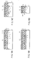
- FIGS. 71A and 71B are side views of a magnetic random access memory of the reference example.
- yoke layers are formed in, e.g., the magnetic random access memory shown in FIG. 73, as shown in FIGS. 71A and 71B.
- the yoke layers include a conductive yoke layer 126 that covers the lower and side surfaces of a write word line 124-1 and a conductive yoke layer 128 that covers the upper and side surfaces of a bit line 113-1 and the side surface of an MTJ element 118.
- an intracell local interconnection 121-1 is formed above the write word line 124-1. For this reason, a thickness t1 of the intracell local interconnection 121-1 and a thickness t2 of a dielectric interlayer which insulates the intracell local interconnection 121-1 from the write word line 124-1 are added between the MTJ element 118 and the write word line 124-1.
- the distance from the memory-layer of the MTJ element 118 to the yoke layer 128 decreases.
- a distance D WWL-M from the memory-layer of the MTJ element 118 to the yoke layer 126 increases.
- FIGS. 72A and 72B are side views of a magnetic random access memory according to the second to fifth embodiments.
- an intracell local interconnection 21-1 is formed below a write word line 24-1.
- An MTJ element 18 is formed on a bit line 13-1. More specifically, the bit line 13-1 is arranged under the MTJ element 18. In addition, an upper surface Stop of the bit line 13-1 is flush with a lower surface Sbtm of the MTJ element 18. For this reason, it is only necessary to set an insulating distance Diso between a yoke layer 28 which covers the upper and side surfaces of the write word line 24-1 and the side surface of the MTJ element 18 and a conductive yoke layer 26 which covers the bottom and side surfaces of the bit line 13-1.
- the memory-layer of the MTJ element 18 can be made closer to the yoke layer 26, as compared to the reference example.
- the distance D BL-M from the memory-layer of the MTJ element 18 to the yoke layer 26 and the distance D WWL-M from the memory-layer of the MTJ element 18 to the yoke layer 28 can substantially equal.
- the distances D BL-M and D WWL-M can substantially equal, the magnetic field generated from the yoke layer 26 and that generated from the yoke layer 28 can be uniformly applied to the memory-layer. For this reason, for example, the magnetic field from the write word line 24-1 and the magnetic field from the bit line 13-1 can be more efficiently applied to the MTJ element 18, as compared to the reference example.
- an adjacent unselected MTJ element 18 is hard to be influenced by the magnetic field from the selected write word line 24-1. For this reason, the reliability related to, e.g., a data write can be further improved.
- the embodiments incorporate inventions of various phases, and the inventions of various phases can be extracted by appropriately combining a plurality of components disclosed in the embodiments.
- the description has been done on the basis of examples in which present invention is applied to a magnetic random access memory.
- the present invention also incorporates a semiconductor integrated circuit device incorporating the above-described magnetic random access memory, e.g., a processor or system LSI.
Landscapes
- Engineering & Computer Science (AREA)
- Chemical & Material Sciences (AREA)
- Nanotechnology (AREA)
- Physics & Mathematics (AREA)
- Mathematical Physics (AREA)
- Theoretical Computer Science (AREA)
- Crystallography & Structural Chemistry (AREA)
- Computer Hardware Design (AREA)
- Mram Or Spin Memory Techniques (AREA)
- Hall/Mr Elements (AREA)
- Semiconductor Memories (AREA)
Applications Claiming Priority (4)
| Application Number | Priority Date | Filing Date | Title |
|---|---|---|---|
| JP2002012640 | 2002-01-22 | ||
| JP2002012640 | 2002-01-22 | ||
| JP2002183983 | 2002-06-25 | ||
| JP2002183983A JP4053825B2 (ja) | 2002-01-22 | 2002-06-25 | 半導体集積回路装置 |
Publications (2)
| Publication Number | Publication Date |
|---|---|
| EP1329950A2 true EP1329950A2 (de) | 2003-07-23 |
| EP1329950A3 EP1329950A3 (de) | 2007-10-10 |
Family
ID=26625590
Family Applications (1)
| Application Number | Title | Priority Date | Filing Date |
|---|---|---|---|
| EP02016245A Withdrawn EP1329950A3 (de) | 2002-01-22 | 2002-07-22 | Magnetoresistives Halbleiterschaltungsbauelement und dessen Verfahren zur Herstellung |
Country Status (6)
| Country | Link |
|---|---|
| US (2) | US6958932B2 (de) |
| EP (1) | EP1329950A3 (de) |
| JP (1) | JP4053825B2 (de) |
| KR (1) | KR100550506B1 (de) |
| CN (1) | CN100476991C (de) |
| TW (1) | TW584940B (de) |
Families Citing this family (18)
| Publication number | Priority date | Publication date | Assignee | Title |
|---|---|---|---|---|
| JP3898556B2 (ja) | 2002-04-22 | 2007-03-28 | 株式会社東芝 | 磁気ランダムアクセスメモリ |
| JP4322481B2 (ja) * | 2002-08-12 | 2009-09-02 | 株式会社東芝 | 半導体集積回路装置 |
| KR100481876B1 (ko) * | 2003-02-20 | 2005-04-11 | 삼성전자주식회사 | 자기 터널 접합을 구비하는 자기 메모리 및 그 제조 방법 |
| US7067866B2 (en) * | 2003-03-31 | 2006-06-27 | Applied Spintronics Technology, Inc. | MRAM architecture and a method and system for fabricating MRAM memories utilizing the architecture |
| US7183130B2 (en) * | 2003-07-29 | 2007-02-27 | International Business Machines Corporation | Magnetic random access memory and method of fabricating thereof |
| WO2005036558A1 (en) * | 2003-10-14 | 2005-04-21 | Agency For Science, Technology And Research | Magnetic memory device |
| KR100634501B1 (ko) | 2004-01-29 | 2006-10-13 | 삼성전자주식회사 | 자기 메모리 소자 및 그 제조방법 |
| US7344896B2 (en) * | 2004-07-26 | 2008-03-18 | Infineon Technologies Ag | Ferromagnetic liner for conductive lines of magnetic memory cells and methods of manufacturing thereof |
| US20060022286A1 (en) * | 2004-07-30 | 2006-02-02 | Rainer Leuschner | Ferromagnetic liner for conductive lines of magnetic memory cells |
| JP4560025B2 (ja) * | 2006-09-29 | 2010-10-13 | 株式会社東芝 | 磁気ランダムアクセスメモリ及びその製造方法 |
| KR100829361B1 (ko) * | 2006-12-26 | 2008-05-13 | 동부일렉트로닉스 주식회사 | 자기 메모리 소자의 제조방법 |
| JP2008227009A (ja) | 2007-03-09 | 2008-09-25 | Toshiba Corp | 磁気ランダムアクセスメモリ、その書き込み方法及びその製造方法 |
| US7911830B2 (en) * | 2007-05-17 | 2011-03-22 | Integrated Magnetoelectronics | Scalable nonvolatile memory |
| KR100944605B1 (ko) * | 2007-12-24 | 2010-02-25 | 주식회사 동부하이텍 | 반도체 소자 |
| US7782660B2 (en) * | 2008-03-20 | 2010-08-24 | International Business Machines Corporation | Magnetically de-coupling magnetic memory cells and bit/word lines for reducing bit selection errors |
| JP2010212661A (ja) * | 2009-02-13 | 2010-09-24 | Fujitsu Ltd | 磁気ランダムアクセスメモリ |
| JP5483281B2 (ja) * | 2010-03-31 | 2014-05-07 | ルネサスエレクトロニクス株式会社 | 半導体装置および半導体装置アセンブリ |
| CN114361201B (zh) * | 2020-10-13 | 2026-03-24 | 联华电子股份有限公司 | 半导体装置 |
Family Cites Families (32)
| Publication number | Priority date | Publication date | Assignee | Title |
|---|---|---|---|---|
| US5902690A (en) * | 1997-02-25 | 1999-05-11 | Motorola, Inc. | Stray magnetic shielding for a non-volatile MRAM |
| US5784311A (en) * | 1997-06-13 | 1998-07-21 | International Business Machines Corporation | Two-device memory cell on SOI for merged logic and memory applications |
| US5956267A (en) | 1997-12-18 | 1999-09-21 | Honeywell Inc | Self-aligned wordline keeper and method of manufacture therefor |
| DE19836567C2 (de) * | 1998-08-12 | 2000-12-07 | Siemens Ag | Speicherzellenanordnung mit Speicherelementen mit magnetoresistivem Effekt und Verfahren zu deren Herstellung |
| US5940319A (en) * | 1998-08-31 | 1999-08-17 | Motorola, Inc. | Magnetic random access memory and fabricating method thereof |
| US5995417A (en) * | 1998-10-20 | 1999-11-30 | Advanced Micro Devices, Inc. | Scheme for page erase and erase verify in a non-volatile memory array |
| JP2000132961A (ja) * | 1998-10-23 | 2000-05-12 | Canon Inc | 磁気薄膜メモリ、磁気薄膜メモリの読出し方法、及び磁気薄膜メモリの書込み方法 |
| US6188105B1 (en) * | 1999-04-01 | 2001-02-13 | Intersil Corporation | High density MOS-gated power device and process for forming same |
| JP3913971B2 (ja) | 1999-12-16 | 2007-05-09 | 株式会社東芝 | 磁気メモリ装置 |
| JP3868699B2 (ja) | 2000-03-17 | 2007-01-17 | 株式会社東芝 | 磁気メモリ装置 |
| KR100418537B1 (ko) | 1999-12-16 | 2004-02-11 | 가부시끼가이샤 도시바 | 자기 메모리 장치 |
| JP2001217398A (ja) * | 2000-02-03 | 2001-08-10 | Rohm Co Ltd | 強磁性トンネル接合素子を用いた記憶装置 |
| US6211090B1 (en) * | 2000-03-21 | 2001-04-03 | Motorola, Inc. | Method of fabricating flux concentrating layer for use with magnetoresistive random access memories |
| DE10113853B4 (de) * | 2000-03-23 | 2009-08-06 | Sharp K.K. | Magnetspeicherelement und Magnetspeicher |
| JP4656720B2 (ja) * | 2000-09-25 | 2011-03-23 | ルネサスエレクトロニクス株式会社 | 薄膜磁性体記憶装置 |
| JP2002208682A (ja) * | 2001-01-12 | 2002-07-26 | Hitachi Ltd | 磁気半導体記憶装置及びその製造方法 |
| JP2003151260A (ja) * | 2001-11-13 | 2003-05-23 | Mitsubishi Electric Corp | 薄膜磁性体記憶装置 |
| TW569442B (en) * | 2001-12-18 | 2004-01-01 | Toshiba Corp | Magnetic memory device having magnetic shield layer, and manufacturing method thereof |
| JP2003197875A (ja) * | 2001-12-28 | 2003-07-11 | Toshiba Corp | 磁気記憶装置 |
| TWI266443B (en) * | 2002-01-16 | 2006-11-11 | Toshiba Corp | Magnetic memory |
| JP4157707B2 (ja) * | 2002-01-16 | 2008-10-01 | 株式会社東芝 | 磁気メモリ |
| US6548849B1 (en) * | 2002-01-31 | 2003-04-15 | Sharp Laboratories Of America, Inc. | Magnetic yoke structures in MRAM devices to reduce programming power consumption and a method to make the same |
| CN100412984C (zh) * | 2002-02-22 | 2008-08-20 | 株式会社东芝 | 磁随机存取存储器 |
| US6873023B2 (en) * | 2002-04-18 | 2005-03-29 | Kabushiki Kaisha Toshiba | Magnetic random access memory |
| US6780653B2 (en) * | 2002-06-06 | 2004-08-24 | Micron Technology, Inc. | Methods of forming magnetoresistive memory device assemblies |
| US6806523B2 (en) * | 2002-07-15 | 2004-10-19 | Micron Technology, Inc. | Magnetoresistive memory devices |
| US6770491B2 (en) * | 2002-08-07 | 2004-08-03 | Micron Technology, Inc. | Magnetoresistive memory and method of manufacturing the same |
| US6740948B2 (en) * | 2002-08-30 | 2004-05-25 | Hewlett-Packard Development Company, L.P. | Magnetic shielding for reducing magnetic interference |
| JP3866641B2 (ja) * | 2002-09-24 | 2007-01-10 | 株式会社東芝 | 磁気記憶装置およびその製造方法 |
| JP3906139B2 (ja) * | 2002-10-16 | 2007-04-18 | 株式会社東芝 | 磁気ランダムアクセスメモリ |
| US6759297B1 (en) * | 2003-02-28 | 2004-07-06 | Union Semiconductor Technology Corporatin | Low temperature deposition of dielectric materials in magnetoresistive random access memory devices |
| JP3831353B2 (ja) * | 2003-03-27 | 2006-10-11 | 株式会社東芝 | 磁気ランダムアクセスメモリ |
-
2002
- 2002-06-25 JP JP2002183983A patent/JP4053825B2/ja not_active Expired - Fee Related
- 2002-07-22 EP EP02016245A patent/EP1329950A3/de not_active Withdrawn
- 2002-07-22 US US10/199,176 patent/US6958932B2/en not_active Expired - Lifetime
- 2002-10-03 TW TW091122835A patent/TW584940B/zh not_active IP Right Cessation
- 2002-10-23 CN CNB021480575A patent/CN100476991C/zh not_active Expired - Fee Related
- 2002-10-30 KR KR1020020066439A patent/KR100550506B1/ko not_active Expired - Fee Related
-
2005
- 2005-06-15 US US11/152,411 patent/US20050274984A1/en not_active Abandoned
Also Published As
| Publication number | Publication date |
|---|---|
| KR100550506B1 (ko) | 2006-02-13 |
| TW584940B (en) | 2004-04-21 |
| US20050274984A1 (en) | 2005-12-15 |
| US20030137028A1 (en) | 2003-07-24 |
| CN100476991C (zh) | 2009-04-08 |
| CN1434455A (zh) | 2003-08-06 |
| JP2003289135A (ja) | 2003-10-10 |
| KR20030063091A (ko) | 2003-07-28 |
| US6958932B2 (en) | 2005-10-25 |
| EP1329950A3 (de) | 2007-10-10 |
| JP4053825B2 (ja) | 2008-02-27 |
Similar Documents
| Publication | Publication Date | Title |
|---|---|---|
| KR100610710B1 (ko) | 자기 랜덤 액세스 메모리 | |
| JP4053825B2 (ja) | 半導体集積回路装置 | |
| KR100537117B1 (ko) | 자기 차폐층을 구비하는 자기 메모리 디바이스 및 그 제조방법 | |
| CN117425389A (zh) | 半导体元件及其制作方法 | |
| US20250113494A1 (en) | Semiconductor device and method for fabricating the same | |
| CN112447788A (zh) | 磁阻式随机存取存储器 | |
| US12408559B2 (en) | Semiconductor device and method for fabricating the same | |
| EP3905250B1 (de) | Halbleiterbauelement und verfahren zur herstellung davon | |
| EP4199688B1 (de) | Halbleiterbauelement und verfahren zur herstellung davon | |
| KR100550484B1 (ko) | 자기 기억 장치의 제조 방법 | |
| US20250366377A1 (en) | Semiconductor device and method for fabricating the same | |
| JP2002319663A (ja) | 半導体記憶装置及びその製造方法 | |
| CN113809117B (zh) | 半导体元件及其制作方法 | |
| JP2004071881A (ja) | 半導体集積回路装置及びその製造方法 | |
| US20250160217A1 (en) | Magnetoresistive random access memory | |
| KR20250107008A (ko) | 가변 저항 메모리 소자 | |
| TW202602343A (zh) | 一種製作磁阻式隨機存取記憶體元件的方法 | |
| TW202545299A (zh) | 磁阻式隨機存取記憶體及其製作方法 | |
| TW202547283A (zh) | 磁阻式隨機存取記憶體及其製作方法 |
Legal Events
| Date | Code | Title | Description |
|---|---|---|---|
| PUAI | Public reference made under article 153(3) epc to a published international application that has entered the european phase |
Free format text: ORIGINAL CODE: 0009012 |
|
| 17P | Request for examination filed |
Effective date: 20020722 |
|
| AK | Designated contracting states |
Designated state(s): AT BE BG CH CY CZ DE DK EE ES FI FR GB GR IE IT LI LU MC NL PT SE SK TR |
|
| AX | Request for extension of the european patent |
Extension state: AL LT LV MK RO SI |
|
| RIC1 | Information provided on ipc code assigned before grant |
Ipc: H01L 43/08 20060101ALN20070524BHEP Ipc: H01L 27/22 20060101ALI20030509BHEP Ipc: H01L 21/8247 20060101AFI20070524BHEP |
|
| PUAL | Search report despatched |
Free format text: ORIGINAL CODE: 0009013 |
|
| AK | Designated contracting states |
Kind code of ref document: A3 Designated state(s): AT BE BG CH CY CZ DE DK EE ES FI FR GB GR IE IT LI LU MC NL PT SE SK TR |
|
| AX | Request for extension of the european patent |
Extension state: AL LT LV MK RO SI |
|
| 17Q | First examination report despatched |
Effective date: 20080403 |
|
| AKX | Designation fees paid |
Designated state(s): DE FR GB |
|
| STAA | Information on the status of an ep patent application or granted ep patent |
Free format text: STATUS: THE APPLICATION IS DEEMED TO BE WITHDRAWN |
|
| 18D | Application deemed to be withdrawn |
Effective date: 20121031 |