EP1326288A2 - Integrierte Halbleiterschaltung und Verfahren zu deren Herstellung - Google Patents
Integrierte Halbleiterschaltung und Verfahren zu deren Herstellung Download PDFInfo
- Publication number
- EP1326288A2 EP1326288A2 EP02258802A EP02258802A EP1326288A2 EP 1326288 A2 EP1326288 A2 EP 1326288A2 EP 02258802 A EP02258802 A EP 02258802A EP 02258802 A EP02258802 A EP 02258802A EP 1326288 A2 EP1326288 A2 EP 1326288A2
- Authority
- EP
- European Patent Office
- Prior art keywords
- semiconductor
- substrate
- integrated circuit
- manufacturing
- semiconductor element
- Prior art date
- Legal status (The legal status is an assumption and is not a legal conclusion. Google has not performed a legal analysis and makes no representation as to the accuracy of the status listed.)
- Ceased
Links
Images


Classifications
-
- H—ELECTRICITY
- H10—SEMICONDUCTOR DEVICES; ELECTRIC SOLID-STATE DEVICES NOT OTHERWISE PROVIDED FOR
- H10H—INORGANIC LIGHT-EMITTING SEMICONDUCTOR DEVICES HAVING POTENTIAL BARRIERS
- H10H20/00—Individual inorganic light-emitting semiconductor devices having potential barriers, e.g. light-emitting diodes [LED]
- H10H20/01—Manufacture or treatment
- H10H20/011—Manufacture or treatment of bodies, e.g. forming semiconductor layers
- H10H20/018—Bonding of wafers
-
- H—ELECTRICITY
- H10—SEMICONDUCTOR DEVICES; ELECTRIC SOLID-STATE DEVICES NOT OTHERWISE PROVIDED FOR
- H10K—ORGANIC ELECTRIC SOLID-STATE DEVICES
- H10K59/00—Integrated devices, or assemblies of multiple devices, comprising at least one organic light-emitting element covered by group H10K50/00
- H10K59/80—Constructional details
- H10K59/875—Arrangements for extracting light from the devices
-
- H—ELECTRICITY
- H10—SEMICONDUCTOR DEVICES; ELECTRIC SOLID-STATE DEVICES NOT OTHERWISE PROVIDED FOR
- H10P—GENERIC PROCESSES OR APPARATUS FOR THE MANUFACTURE OR TREATMENT OF DEVICES COVERED BY CLASS H10
- H10P90/00—Preparation of wafers not covered by a single main group of this subclass, e.g. wafer reinforcement
- H10P90/19—Preparing inhomogeneous wafers
- H10P90/1904—Preparing vertically inhomogeneous wafers
- H10P90/1906—Preparing SOI wafers
- H10P90/1914—Preparing SOI wafers using bonding
-
- H—ELECTRICITY
- H10—SEMICONDUCTOR DEVICES; ELECTRIC SOLID-STATE DEVICES NOT OTHERWISE PROVIDED FOR
- H10W—GENERIC PACKAGES, INTERCONNECTIONS, CONNECTORS OR OTHER CONSTRUCTIONAL DETAILS OF DEVICES COVERED BY CLASS H10
- H10W70/00—Package substrates; Interposers; Redistribution layers [RDL]
- H10W70/01—Manufacture or treatment
- H10W70/05—Manufacture or treatment of insulating or insulated package substrates, or of interposers, or of redistribution layers
- H10W70/093—Connecting or disconnecting other interconnections thereto or therefrom, e.g. connecting bond wires or bumps
-
- H—ELECTRICITY
- H10—SEMICONDUCTOR DEVICES; ELECTRIC SOLID-STATE DEVICES NOT OTHERWISE PROVIDED FOR
- H10K—ORGANIC ELECTRIC SOLID-STATE DEVICES
- H10K59/00—Integrated devices, or assemblies of multiple devices, comprising at least one organic light-emitting element covered by group H10K50/00
- H10K59/80—Constructional details
- H10K59/87—Passivation; Containers; Encapsulations
- H10K59/873—Encapsulations
-
- H—ELECTRICITY
- H10—SEMICONDUCTOR DEVICES; ELECTRIC SOLID-STATE DEVICES NOT OTHERWISE PROVIDED FOR
- H10P—GENERIC PROCESSES OR APPARATUS FOR THE MANUFACTURE OR TREATMENT OF DEVICES COVERED BY CLASS H10
- H10P72/00—Handling or holding of wafers, substrates or devices during manufacture or treatment thereof
- H10P72/70—Handling or holding of wafers, substrates or devices during manufacture or treatment thereof for supporting or gripping
- H10P72/74—Handling or holding of wafers, substrates or devices during manufacture or treatment thereof for supporting or gripping using temporarily an auxiliary support
- H10P72/7428—Handling or holding of wafers, substrates or devices during manufacture or treatment thereof for supporting or gripping using temporarily an auxiliary support used to support diced chips prior to mounting
-
- H—ELECTRICITY
- H10—SEMICONDUCTOR DEVICES; ELECTRIC SOLID-STATE DEVICES NOT OTHERWISE PROVIDED FOR
- H10P—GENERIC PROCESSES OR APPARATUS FOR THE MANUFACTURE OR TREATMENT OF DEVICES COVERED BY CLASS H10
- H10P72/00—Handling or holding of wafers, substrates or devices during manufacture or treatment thereof
- H10P72/70—Handling or holding of wafers, substrates or devices during manufacture or treatment thereof for supporting or gripping
- H10P72/74—Handling or holding of wafers, substrates or devices during manufacture or treatment thereof for supporting or gripping using temporarily an auxiliary support
- H10P72/7434—Handling or holding of wafers, substrates or devices during manufacture or treatment thereof for supporting or gripping using temporarily an auxiliary support used in a transfer process involving at least two transfer steps, i.e. including an intermediate handle substrate
-
- H—ELECTRICITY
- H10—SEMICONDUCTOR DEVICES; ELECTRIC SOLID-STATE DEVICES NOT OTHERWISE PROVIDED FOR
- H10W—GENERIC PACKAGES, INTERCONNECTIONS, CONNECTORS OR OTHER CONSTRUCTIONAL DETAILS OF DEVICES COVERED BY CLASS H10
- H10W70/00—Package substrates; Interposers; Redistribution layers [RDL]
- H10W70/099—Connecting interconnections to insulating or insulated package substrates, interposers or redistribution layers
-
- H—ELECTRICITY
- H10—SEMICONDUCTOR DEVICES; ELECTRIC SOLID-STATE DEVICES NOT OTHERWISE PROVIDED FOR
- H10W—GENERIC PACKAGES, INTERCONNECTIONS, CONNECTORS OR OTHER CONSTRUCTIONAL DETAILS OF DEVICES COVERED BY CLASS H10
- H10W72/00—Interconnections or connectors in packages
- H10W72/071—Connecting or disconnecting
- H10W72/073—Connecting or disconnecting of die-attach connectors
- H10W72/07302—Connecting or disconnecting of die-attach connectors using an auxiliary member
- H10W72/07304—Connecting or disconnecting of die-attach connectors using an auxiliary member the auxiliary member being temporary, e.g. a sacrificial coating
-
- H—ELECTRICITY
- H10—SEMICONDUCTOR DEVICES; ELECTRIC SOLID-STATE DEVICES NOT OTHERWISE PROVIDED FOR
- H10W—GENERIC PACKAGES, INTERCONNECTIONS, CONNECTORS OR OTHER CONSTRUCTIONAL DETAILS OF DEVICES COVERED BY CLASS H10
- H10W72/00—Interconnections or connectors in packages
- H10W72/071—Connecting or disconnecting
- H10W72/073—Connecting or disconnecting of die-attach connectors
- H10W72/07331—Connecting techniques
-
- H—ELECTRICITY
- H10—SEMICONDUCTOR DEVICES; ELECTRIC SOLID-STATE DEVICES NOT OTHERWISE PROVIDED FOR
- H10W—GENERIC PACKAGES, INTERCONNECTIONS, CONNECTORS OR OTHER CONSTRUCTIONAL DETAILS OF DEVICES COVERED BY CLASS H10
- H10W90/00—Package configurations
-
- H—ELECTRICITY
- H10—SEMICONDUCTOR DEVICES; ELECTRIC SOLID-STATE DEVICES NOT OTHERWISE PROVIDED FOR
- H10W—GENERIC PACKAGES, INTERCONNECTIONS, CONNECTORS OR OTHER CONSTRUCTIONAL DETAILS OF DEVICES COVERED BY CLASS H10
- H10W90/00—Package configurations
- H10W90/701—Package configurations characterised by the relative positions of pads or connectors relative to package parts
- H10W90/731—Package configurations characterised by the relative positions of pads or connectors relative to package parts of die-attach connectors
- H10W90/734—Package configurations characterised by the relative positions of pads or connectors relative to package parts of die-attach connectors between a chip and a stacked insulating package substrate, interposer or RDL
-
- H—ELECTRICITY
- H10—SEMICONDUCTOR DEVICES; ELECTRIC SOLID-STATE DEVICES NOT OTHERWISE PROVIDED FOR
- H10W—GENERIC PACKAGES, INTERCONNECTIONS, CONNECTORS OR OTHER CONSTRUCTIONAL DETAILS OF DEVICES COVERED BY CLASS H10
- H10W99/00—Subject matter not provided for in other groups of this subclass
Definitions
- the present invention relates to semiconductor integrated circuits, methods for manufacturing semiconductor integrated circuits, semiconductor element members, electrooptic devices, and electronic devices. More specifically, the present invention relates to a method for transferring a semiconductor element onto an object having material properties different from those of the semiconductor element, such as a substrate.
- Such techniques include, for instance, formation of a vertical cavity surface emitting laserdiode (VCSEL), a photodiode (PD), or a high electron mobility transistor (HEMT) on a silicon semiconductor substrate, and attachment of a micro-silicon transistor, instead of a thin film transistor (TET) of each pixel of a liquid crystal display (LCD), onto a glass substrate.
- VCSEL vertical cavity surface emitting laserdiode
- PD photodiode
- HEMT high electron mobility transistor
- Examples of the integrated circuits including such a semiconductor having different material properties include an optoelectronic integrated circuit (OEIC).
- OEIC optoelectronic integrated circuit
- the optoelectronic integrated circuit is an integrated circuit having an optical input/output means. Signal processing in the OEIC is electrically performed whereas light is used for input and output processes of the OEIC.
- silicon is an indirect transition semiconductor, it cannot emit light by itself. Accordingly, it is necessary to form an integrated circuit by combining silicon with another semiconductor light emitting diode.
- the VCSEL made from a GaAs compound semiconductor, etc. may be favorably used as a semiconductor light emitting diode.
- a semiconductor process such as epitaxy, since the VCSEL does not match the lattice structure of silicon.
- the VCSEL is formed on a GaAs substrate.
- a method has been considered in which an electric signal transmission circuit is merged with an optical signal transmission circuit by making the VCSEL on the GaAs substrate into a chip and mechanically mounting the chip on a silicon integrated circuit substrate.
- the size of the VCSEL chip on an integrated circuit be as small as possible from the viewpoint of effectively using the surface of the semiconductor substrate on which the integrated circuit is formed, and of readiness in handling the chip after merging. It is ideal for the size of the chip to be about the same size as a monolithic integrated circuit, i.e., dimensions of a few ⁇ m in thickness x a few tens of ⁇ m 2 in surface area. However, according to convention semiconductor mounting techniques, the size of a chip that can be handled is greater than a few tens of ⁇ m in thickness x a few hundreds of ⁇ m 2 in surface area.
- a semiconductor layer (a functional layer) a few pin thick, which becomes a target semiconductor element, is formed on a desired position of the final substrate. This is processed using a normal semiconductor process, and is made into a product by attaching electrodes, etc.
- the present invention takes into consideration the above-mentioned circumstances, and it has as an object to solve the above problems generated when a semiconductor element is formed on an object having material properties different from those of the semiconductor element to improve the efficiency in using the semiconductor substrate on which the semiconductor element is formed, and to provide semiconductor integrated circuits, methods for manufacturing the semiconductor integrated circuit, semiconductor element members, electrooptic devices, and electronic devices by which unnecessary activity in the manufacturing process of the integrated circuit can be reduced.
- the first aspect of the present invention provides a method for manufacturing a semiconductor integrated circuit, comprising the steps of: forming a semiconductor element on a semiconductor substrate; and separating only a function layer including the semiconductor element, which is a surface layer of the semiconductor substrate, from the semiconductor substrate.
- the semiconductor element may be a compound semiconductor, or silicon semiconductor
- the object to which the semiconductor element is joined may be a silicon semiconductor substrate, a compound semiconductor substrate, or other substances.
- the semiconductor elements are separated in the shape of micro tiles after they are completed on the semiconductor substrate, it becomes possible to conduct a selection test on the semiconductor elements prior to forming an integrated circuit.
- the present invention also provides a method for manufacturing a semiconductor integrated circuit, comprising the steps of: forming a semiconductor element on a semiconductor substrate; attaching a film member on a surface of the semiconductor substrate on which the semiconductor element is formed; and separating a function layer of the semiconductor substrate including the semiconductor element from the semiconductor substrate.
- the functional layer including the semiconductor element may be separated from the semiconductor substrate in the shape of micro tiles, and they can be handled by mounting on the film member, it becomes possible to individually select the semiconductor elements to be joined to a final substrate, and to decrease the size of the semiconductor element that can be handled as compared with that of conventional mounting techniques.
- the semiconductor element be a compound semiconductor device including at least one of a light emitting diode, a vertical cavity surface emitting laserdiode, a photodiode, a high electron mobility transistor, an inductor, a capacitor, a resistor, and a heterojunction bipolar transistor.
- the semiconductor element be a silicon semiconductor device including at least one of an integrated circuit, a photodiode, a transistor, and a diode.
- the above method for manufacturing a semiconductor integrated circuit further includes the step of joining the functional layer attached to the film member onto a substrate made of silicon, quartz, sapphire, metals, ceramics, or plastic films.
- the semiconductor substrate in the above method for manufacturing a semiconductor integrated circuit, includes a sacrificial layer disposed below the functional layer, and the functional layer is separated from the semiconductor substrate by etching the sacrificial layer.
- the semiconductor substrate include a gallium-arsenic compound semiconductor
- the sacrificial layer includes an aluminum-arsenic compound semiconductor, an aluminum-gallium-arsenic compound semiconductor, an indium-phosphorus compound semiconductor, or an indium-gallium-phosphorus compound semiconductor.
- the semiconductor substrate be formed as a Silicon-On-Insulator substrate, and that the sacrificial layer include a silicon oxide membrane.
- the above method for manufacturing a semiconductor integrated circuit further include the step of: forming separation grooves on the semiconductor substrate, wherein the functional layer is separated from the semiconductor substrate by using the separation grooves and etching the sacrificial layer.
- the separation groove be formed by using a dry etching process or wet etching process.
- each of the separation grooves have a depth sufficient to reach at least the sacrificial layer.
- the sacrificial layer be etched using low concentration hydrochloric acid, hydrogen fluoride, or buffered hydrogen fluoride.
- the present invention also provides a method for manufacturing a semiconductor integrated circuit, including the steps of: forming a semiconductor element on a semiconductor substrate, the semiconductor substrate including a sacrificial layer that may be removed by an etching process; forming separation grooves on the semiconductor substrate, each of the separation grooves having a depth sufficient to reach at least the sacrificial layer; attaching a film member on a surface of the semiconductor substrate; and separating the semiconductor element from the semiconductor substrate by supplying an etching solution to the separation grooves to etch the sacrificial layer.
- the above method for manufacturing a semiconductor integrated circuit further include the step of joining the semiconductor element attached to the film member to a substrate different from the semiconductor substrate.
- the above method for manufacturing a semiconductor integrated circuit further include the step of connecting the semiconductor element, which is joined to the substrate, to a circuit formed on the substrate.
- the present invention also provides a semiconductor element member, including a semiconductor element; and a film member attached to the semiconductor element, wherein the semiconductor element member is produced by a method comprising the steps of: forming the semiconductor element on a semiconductor substrate; separating the semiconductor element from the semiconductor substrate; and attaching the film member onto the semiconductor element.
- the present invention also provides a semiconductor integrated circuit including the above semiconductor element member, and a substrate, which is different from the semiconductor substrate used for forming the semiconductor element, on which the semiconductor element member is mounted, wherein the semiconductor element member is produced by a method comprising the steps of joining the semiconductor element member to the substrate, and connecting the semiconductor element to a circuit of the substrate.
- the present invention also provides an electrooptic device including the above semiconductor integrated circuit.
- the present invention also provides an electrooptic device including at least one of the functional layer produced by the above method, and the semiconductor element produced by the above method.
- the above electrooptic device further include a plurality of scan lines and data lines which are formed in a matrix; a switching device connected to the scan lines and data lines; and a pixel electrode connected to the switching device.
- the above electrooptic device further include a light emitting element.
- the present invention also provides an electronic device including the above electrooptic device.
- semiconductor substrate used in the embodiments of the present invention means an object made of a semiconductor material.
- the shape of the semiconductor substrate is not particularly limited, and a semiconductor material having other than a plate shape is included in the "semiconductor substrate".
- FIG. 1 is a diagram showing a schematic cross-sectional view for explaining the first step of a method for manufacturing a semiconductor integrated circuit according to the embodiment of the present invention.
- a substrate 10 is a semiconductor substrate, and in this embodiment, the substrate 10 is a GaAs compound semiconductor substrate.
- a sacrificial layer 11 is disposed as the lowest layer in the substrate 10.
- the sacrificial layer 11 is made of aluminum-arsenic (AlAs) and has a thickness of about several hundred nm, for example.
- AlAs aluminum-arsenic
- a functional layer 12 may be disposed on the sacrificial layer 11.
- the thickness of the functional layer 12 is, for instance, between about 1 to 20 ⁇ m.
- a semiconductor device (semiconductor element) 13 is formed on the functional layer 12.
- the semiconductor device 13 include, for instance, a light emitting diode (LED), a vertical cavity surface emitting laserdiode (VCSEL), a photodiode (PD), a high electron mobility transistor (HEMT), and a high electron mobility transistor (HEMT).
- LED light emitting diode
- VCSEL vertical cavity surface emitting laserdiode
- PD photodiode
- HEMT high electron mobility transistor
- HEMT high electron mobility transistor
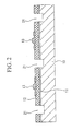
- FIG. 2 is a diagram showing a schematic cross-sectional view for explaining the second step of the method for manufacturing a semiconductor integrated circuit according to the embodiment of the present invention.
- separation grooves 21 are formed so as to divide each of the semiconductor devices 13.
- Each separation groove 21 has a depth deep enough to reach at least the sacrificial layer 11. Both the width and depth of the separation groove 21 may be, for instance, in the range of about 10 to several hundred ⁇ m.
- the separation grooves 21 are connected to each other so that a selective etching solution, which will be described later, will flow in the separation grooves 21.
- the distance between the separation grooves 21 is adjusted to be about several tens to several hundred ⁇ m so that each of the semiconductor devices 21 divided and separated by the separation grooves 21 have a size of about several tens to several hundred ⁇ m 2 .
- the separation grooves 21 may be formed using a photolithography method combined with a wet etching method, or a dry etching method. Moreover, the separation grooves 21 may also be formed by dicing of a U-shape groove as long as no cracks are generated on the substrate.
- a sulfuric acid type etching solution may be used for wet etching, and a chlorine gas may be used for dry etching Since the pattern dimension of the separation groove 21 is large and accuracy is not very important, etching masks need not be formed using the photolithography. That is, the etching masks may be formed using, for instance, the offset printing. In the formation of the separation grooves 21, the direction of the separation grooves 21 with respect to the crystal orientation of the substrate 10 is important.
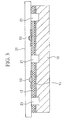
- FIG. 3 is a diagram showing a schematic cross-sectional view for explaining the third step of the method for manufacturing a semiconductor integrated circuit according to the embodiment of the present invention.
- an intermediate transfer film 31 is attached to a surface (the semiconductor device 13 side) of the substrate 10.
- the intermediate transfer film 31 is a flexible band-shape film, the surface of which is coated with an adhesive.
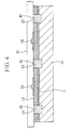
- FIG. 4 is a diagram showing a schematic cross-sectional view for explaining the fourth step of the method for manufacturing a semiconductor integrated circuit according to the embodiment of the present invention.
- a selective etching solution 41 is filled in the separation grooves 21.
- low concentration hydrochloric acid having high selectivity to aluminum-arsenic is used as the selective etching solution 41.
- hydrochloric acid from the viewpoint of selectivity.
- FIG. 5 is a diagram showing a schematic cross-sectional view for explaining the fifth step of the method for manufacturing a semiconductor integrated circuit according to the embodiment of the present invention.
- this step after a predetermined period of time has elapsed since the application of the selective etching solution 41 to the separation grooves 21 in the fourth step, the whole sacrificial layer 11 is removed from the substrate 10 using the selective etching process. After this, pure water is introduced to the portions where the separation grooves 32 and the sacrificial layer 11 were present to rinse the portions.
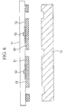
- FIG. 6 is a diagram showing a schematic cross-sectional view for explaining the sixth step of the method for manufacturing a semiconductor integrated circuit according to the embodiment of the present invention.
- the functional layers 12 are separated from the substrate 10.
- the functional layers 12 attached to the intermediate transfer film 31 are separated from the substrate 10 by separating the intermediate transfer film 31 from the substrate 10.
- the functional layers 12 on which the semiconductor devices 13 are formed are separated by the formation of the separation grooves 21 and the etching of the sacrificial layer 11 to be formed as a semiconductor element of a predetermined shape, for instance, a micro tile shape, which will also be referred to as a micro tile element 61 hereinafter, and are attached and supported by the intermediate transfer film 31.
- the thickness of the functional layer be in the range of about 1 to 8 ⁇ m, and the dimensions (i.e., length and width) thereof be in the range of about several tens to several hundred ⁇ m, for instance.
- the substrate 10, from which the functional layers 12 are separated for the formation of another semiconductor device.
- the above-mentioned first to sixth steps may be repeated by providing a plurality of the sacrificial layers 11 in advance, and hence, the micro tile elements 61 may be repeatedly produced.
- FIG. 7 is a diagram showing a schematic cross-sectional view for explaining the seventh step of the method for manufacturing a semiconductor integrated circuit according to the embodiment of the present invention.
- the micro tile elements 61 are aligned at desired positions on a final substrate 71 by transferring the intermediate transfer film 31 to which the micro tile elements 61 are attached.
- the final substrate 71 is made of a silicon semiconductor, and an LSI area 72 has been provided with the final substrate 71.
- an adhesive 73 for adhering the micro tile elements 61 is applied to desired positions on the final substrate 71.
- FIG. 8 is a diagram showing a schematic cross-sectional view for explaining the eighth step of the method for manufacturing a semiconductor integrated circuit according to the embodiment of the present invention.
- the micro tile elements 61 which have been aligned at desired positions on the final substrate 71, are pressed against the final substrate 71 via the intermediate transfer film 31 using a collet 81 so that the micro tile elements 61 are joined to the final substrate 71.
- the adhesive 73 is applied to the desired positions on the final substrate 71, the micro tile elements 61 are attached to the desired positions on the final substrate 71.
- the adhesive is used as a means for adhering the micro tile elements 61 on the final substrate 71, it is possible to use other adhering means.
- FIG. 9 is a diagram showing a schematic cross-sectional view for explaining the ninth step of the method for manufacturing a semiconductor integrated circuit according to the embodiment of the present invention.
- the intermediate transfer film 31 is separated from the micro tile elements 61 by eliminating the adhesive power from the intermediate transfer film 31.
- a UV curable adhesive or a thermosetting adhesive may be used for the adhesive on the intermediate transfer film 31.
- the collet 81 is made of a transparent material so that the adhesive power of the intermediate transfer film 31 may be eliminated by irradiating ultraviolet (UV) rays from an end of the collet 81.
- UV ultraviolet
- the thermosetting adhesive it is sufficient to heat the collet 81 to eliminate the adhesive power.
- micro tile elements 61 are firmly joined to the final substrate 71 by subjecting them to a heating process, etc.
- FIG. 10 is a diagram showing a schematic cross-sectional view for explaining the eleventh step of the method for manufacturing a semiconductor integrated circuit according to the embodiment of the present invention.
- the electrodes of the micro tile elements 61 are electrically connected to the circuit on the final substrate 71 via wiring 91 to form a LSI chip.
- the final substrate 71 not only the silicon semiconductor but also a quartz substrate or a plastic film may be applied.
- the silicon semiconductor is applied as the final substrate 71, it is possible to make it a substrate having a charge coupled device (CCD).
- CCD charge coupled device
- a glass substrate, such as one of quartz is applied as the final substrate 71, it may be used for liquid crystal displays (LCDs) or organic electroluminescent displays.
- the plastic film is applied as the final substrate 71, this may be used for LCDs, organic electroluminescent panels, or IC film packages.
- the first to eleventh steps of the second embodiment correspond to the first to eleventh steps of the first embodiment.
- the significant difference between the first and second embodiments is that the method used for selectively etching the sacrificial layer in the fourth step is different.
- a silicon transistor is formed on a silicon-on-insulator (SOI) substrate using an ordinary process.
- SOI silicon-on-insulator
- a silicon oxide membrane which becomes a sacrificial layer is provided with the SOI substrate.
- separation grooves are formed on the SOI substrate.
- Each separation groove has a depth deep enough to reach at least the silicon oxide membrane which becomes the sacrificial layer in the SOI substrate.
- the separation grooves may be formed using a method, such as an etching.
- an intermediate transfer film is attached to a surface (the silicon transistor side) of the SOI substrate.
- hydrogen fluoride is introduced to the separation groove in order to selectively etch only the silicon oxide membrane which forms the sacrificial layer.
- the sacrificial layer made of the silicon oxide membrane is etched to separate the silicon transistor (silicon semiconductor element) from the silicon substrate.
- the silicon transistor attached to the intermediate transfer film is separated from the SOI substrate by separating the intermediate transfer film from the SOI substrate.
- the silicon transistors are aligned at desired positions on the final substrate by moving the intermediate transfer film.
- a glass substrate for liquid crystal is used as the final substrate.
- the silicon transistors aligned at desired positions on the final substrate are joined to the final substrate by pressing against the final substrate via the intermediate transfer film using a collet.
- each of the silicon transistors is adhered to the desired position on the final substrate.
- the adhesive power of the intermediate transfer film is eliminated to separate the intermediate transfer film from the silicon transistor.
- the silicon transistor is completely joined to the final substrate by subjecting the transistor to a heating process, and so forth.
- the electrodes of the transistor are connected to the circuit on the final substrate via wiring to form the glass substrate for liquid crystal, a driving circuit therefor, and so forth.
- FIG. 18 is a diagram showing a schematic perspective view of an example of conventional hybrid integrated circuits.
- a silicon LSI chip 111 includes a LSI area 112.
- a photodiode chip 101a, a VCSEL chip 101b, and a HEMT chip 101c are joined to the surface of the silicon LSI chip 111.
- the limit in size of the chip that can be handled using the conventional mounting techniques is thickness of several tens ⁇ m x surface area of several hundreds ⁇ m 2 . Accordingly, the size of the photodiode chip 101a, the VCSEL chip 101b, and the HEMT chip 101c become greater than the thickness of several tens ⁇ m x surface area of several hundreds ⁇ m 2 .
- FIG 11 is a schematic perspective view showing an example of the integrated circuits which are manufactured by using the method for manufacturing the semiconductor integrated circuit according to an embodiment of the present invention.
- the silicon LSI chip which is the final substrate 71, includes the LSI area 72.
- a photodiode tile 61a, a VCSEL tile 61b, and a high performance transistor tiles 61c are joined to the surface of the final substrate 71.
- the HBT means a compound semiconductor heterojunction bipolar transistor.
- the photodiode tile 61a, the VCSEL tile 61b, and the high performance transistor tile 61 c are manufactured as the micro tile elements 61 and are joined using the manufacturing method according to the first embodiment of the present invention. Accordingly, it is possible to realize the dimensions (thickness of several ⁇ m x surface area of several tens of ⁇ m 2 ) for the photodiode tile 61a, the VCSEL tile 61b, and the high performance transistor 61c.
- a semiconductor element i.e., the micro tile element 61
- an arbitrary kind of substrate such as silicon, quartz, sapphire, metals, ceramics, and plastic films.
- a test can be performed on a semiconductor element in advance and the semiconductor may be selected based on the result of the test since the semiconductor element (the semiconductor device 13) is processed to be the micro tile element 61 after the semiconductor element is formed on the semiconductor substrate (the substrate 10).
- the whole semiconductor substrate (the substrate 10) from which the micro tile elements 61 are produced can be used for the semiconductor devices 13 except the portion that is used for the separation grooves. Accordingly, it becomes possible to increase the efficiency in using the area of the semiconductor substrate (the substrate 10), and to reduce the manufacturing cost.
- each of the micro tile elements 61 may be selected and joined to the final substrate 71.
- the micro tile elements 61 are joined to the final substrate 71 in a completed state as a semiconductor element, a complicated semiconductor process is not required after the joining process. Accordingly, it is not necessary to treat the whole final substrate 71 after the micro tile elements 61 are joined to the final substrate 71, and hence, it becomes possible to reduce the unnecessary activity in the manufacturing process.
- a vertical cavity surface emitting laserdiode (VCSEL) and a photodiode (PD) are disposed on a silicon LSI using the above method according to the first embodiment of the present invention.
- VCSEL vertical cavity surface emitting laserdiode
- PD photodiode
- a high performance transistor e.g. HBT
- a silicon LSI using the above method according to the first embodiment of the present invention.
- the length of wiring can be shortened, and hence, high performance of the circuits can be realized.
- the whole semiconductor substrate (the substrate 10) from which the micro tile elements 61 are produced, can be used as the semiconductor devices 13 except the portion that is used for the separation grooves 21. Accordingly, it becomes possible to increase the efficiency in using the area of the AgAs substrate, which is expensive, and to reduce the manufacturing cost.
- a micro-silicon transistor instead of a thin film transistor (TFT) is attached using the manufacturing method according to the present invention. That is, the silicon transistors are attached to a glass substrate for liquid crystal by using the above-mentioned method according to the second embodiment of the present invention. In this manner, it becomes possible to obtain a switching function, the performance of which is better compared to the case where the TFT is employed. Since the proportion of the area of the transistor in a pixel of a liquid crystal display is only a few percent, the rest of the pixel area other than the TFT area becomes useless if the entire surface of the pixel is formed using a TFT process.
- TFT thin film transistor
- Electrooptic Device As each pixel of an organic electroluminescent device, which is an electrooptic device, a micro-silicon transistor, instead of a thin film transistor (TFT), is attached using the manufacturing method according to the present invention.
- TFT thin film transistor
- FIG. 12 is a diagram showing a cross-sectional view of an example of the electroluminescent devices which is an electrooptic device according to the embodiment of the present invention.
- an organic electroluminescent device 1 includes an optically transparent substrate (light permeable layer) 2, and an organic electroluminescent element (light emitting element) 9 including a light emitting layer 5 and a positive hole transporting layer 6.
- the light emitting layer 5 is disposed between a pair of electrodes (a cathode 7 and an anode 8) and is made of an organic electroluminescent material.
- a low refractive index layer 3, and a sealing layer 4 may be laminated between the substrate 2 and the organic electroluminescent element 9, The low refractive index layer 3 is disposed closer to the substrate 2 as compared to the sealing layer 4.
- a sealing member 320 which prevents air from entering the organic electroluminescent element 9, is disposed on a surface opposite the sealing layer 4 as shown in FIG. 13.
- the organic electroluminescent device 1 may be produced by forming the anode 8 on the sealing layer 4 using sputtering, ion-plating, or a vacuum vapor deposition method, and vapor depositing and laminating the positive hole transporting layer 6, the light emitting layer 5, and the cathode 7 in that order on the anode 8.
- the materials that can be used for forming the substrate 2 include a transparent or translucent material through which light may pass, for instance, a transparent glass, quartz, sapphire, or transparent synthetic resins, such as polyester, polyacrylate, polycarbonate, and polyetherketone.
- a soda-lime glass which is inexpensive may be suitably used as a material for forming the substrate 2.
- the substrate 2 may be made of an opaque substance.
- ceramics such as alumina
- a sheet of metal such as stainless steel, which is subjected to an insulating treatment like surface oxidation, thermosetting resins, and thermoplastic resins may be suitably used.
- the anode 8 is a'transparent electrode made of indium tin oxide (ITO), for example, and light can be transmitted through the anode 8.
- the positive hole transporting layer 6 may be made of, for instance, triphenylamine derivative (TPD), pyrazoline derivative, arylamine derivative, stilbene derivative, and triphenyldiamine derivative. More specifically, examples of the anode 8 include those disclosed in Japanese Unexamined Patent Application, First publication No. Sho 63-70257, Japanese Unexamined Patent Application, First publication No. Sho 63-175860, Japanese Unexamined Patent Application, First publication No. Hei 2-135359, Japanese Unexamined Patent Application, First publication No. Hei 2-135361, Japanese Unexamined Patent Application, First publication No.
- a positive hole injection layer may be formed instead of the positive hole transporting layer, and it is possible to form both the positive hole injection layer and the positive hole transporting layer.
- the materials that may be used for forming the positive hole injection hole include, for instance, copper phthalocyanine (CuPc), polyphenylenevinylene which is a polytetrahydrothiophenylphenylene, 1,1-bis-(4-N,N-ditolylaminophenyl)cyclohexane, and tris(8-hydroxyquinolinol).
- CuPc copper phthalocyanine
- CuPc copper phthalocyanine
- Non-limiting examples of the materials that may be used for forming the light emitting layer 5 include, for instance, low molecular organic light emitting pigments and high molecular light emitting materials, i.e., various fluorescent substances and phosphorescent substances, and organic electroluminescent materials, such as Alq 3 (aluminum chelate complexes).
- organic electroluminescent materials such as Alq 3 (aluminum chelate complexes).
- conjugated polymers which function as light emitting materials use of one which includes an arylenevinylene or polyfluorene structure is particularly preferable.
- the cathode 7 is a metal electrode made of aluminum (AI), magnesium (Mg), gold (Au), silver (Ag) and so forth.
- an electron transporting layer or an electron injection layer between the cathode 7 and the light emitting layer 5.
- Materials that can be used for forming the electron transporting layer are not particularly limited, and examples of such materials include, for instance, oxadiazole derivatives, anthraquinodimethane and its derivatives, benzoquinone and its derivatives, naphthoquinone and its derivatives, anthraquinone and its derivatives, tetracyanoanthraquinodimethane and its derivatives, fluorenone derivatives, diphenyldicyanoethylene and its derivatives, diphenoquinone derivatives, and metal complexes of 8-hydroxyquinoline and its derivatives.
- examples of the materials that can be used for the electron transporting layer include those disclosed in Japanese Unexamined Patent Application, First publication No. Sho 63-70257, Japanese Unexamined Patent Application, First publication No. Sho 63-175860, Japanese Unexamined Patent Application, First publication No. Hei 2-135359, Japanese Unexamined Patent Application, First publication No. Hei 2-135361, Japanese Unexamined Patent Application, First publication No. Hei 2-209988, Japanese Unexamined Patent Application, First publication No. Hei 3-37992, and Japanese Unexamined Patent Application, First publication No. Hei 3-152184.
- the organic electroluminescent device 1 is of an active matrix type, and in practice, a plurality of data lines and scan lines are arranged on the substrate 2 in a grid.
- an organic electroluminescent element is connected to each pixel, which is divided by the data lines and the scan lines to be disposed in a matrix, via driving TFTs, such as switching transistors and driving transistors.
- driving TFTs such as switching transistors and driving transistors.
- micro silicon transistors of the present invention are attached to each pixel instead of the driving TFTs, such as the switching transistors and the driving transistors, conventionally provided with each pixel.
- the attachment of the micro silicon transistors is carried out using the above-mentioned first to eleventh steps of the manufacturing method according to the embodiment of the present invention.
- FIG. 14 is a diagram showing a case where the electrooptic device according to the embodiment of the present invention is applied to an active matrix type display device (an electrooptic device) using electroluminescent elements.
- FIG. 14 which is a circuit diagram
- a plurality of scan lines 131, a plurality of signal lines 132 extending in directions crossing the scan lines 131, and a plurality of common feed lines 133 extending in directions parallel to the signal lines 132 are arranged on the substrate.
- a pixel (a pixel area element) AR is formed at each of the position where the scan line 131 crosses the signal line 132.
- a data line driving circuit 390 having a shift register, a level shifter, a video line, and an analog switch is provided for the signal lines 132.
- a scan line driving circuit 380 including a shift register and a level shifter is provided with the scan line 131.
- a first transistor 322, a retention volume cap, a second transistor 324, a pixel electrode 323, and a light emitting portion (light emitting layer) 360 are provided in each of the pixel area AR.
- a scan signal is supplied to a gate via the scan line 131.
- the retention volume cap retains an image signal supplied from the signal line 132 via the first transistor 322.
- the image signal retained by the retention volume cap is supplied to a gate of the second transistor 324.
- a driving current flows to the pixel electrode 323 from the common feed lines 133 via the second transistor 324 when the pixel electrode 323 is electrically connected to the common feed lines 133.
- the light emitting portion 360 is disposed between the pixel electrode 323, which functions as an anode, and a common electrode 222, which functions as a cathode.
- the first transistor 322, and the second transistor 324 are micro silicon transistors which are attached to a substrate of the electroluminescent display device manufactured by using the above explained first to eleventh steps according to the present invention.
- the light emitting layer 360 emits light in accordance with the amount of current which flows through the light emitting layer 360.
- FIG. 15 is a diagram showing a perspective view of a mobile phone, which is an example of the electronic devices according to the embodiment of the present invention.
- the reference numeral 1000 indicates a body of the mobile phone
- the reference numeral 1001 indicates a display portion to which the above-mentioned electrooptic device of the present invention has been applied.
- FIG 16 is a diagram showing a perspective view of a wristwatch type electronic device, which is another example of the electronic devices according to the embodiment of the present invention.
- the reference numeral 1100 indicates a body of the watch
- the reference numeral 1101 indicates a display portion to which the above-mentioned electrooptic device of the present invention has been applied.
- FIG 17 is a diagram showing a perspective view of a portable information processing device, such as a word processor and a personal computer, which is an example of the electronic devices according to the embodiment of the present invention.
- the reference numeral 1200 indicates an information processing device
- the reference numeral 1202 indicates an input unit, such as a keyboard
- the reference numeral 1204 indicates a body of the information processing device
- the reference numeral 1206 indicates a display portion to which the above-mentioned electrooptic device of the present invention has been applied.
- each of the devices has an excellent display grade, and in particular, an electronic device having an electroluminescent display unit, which includes a high-response, and bright screen, may be realized. Also, by using the manufacturing method according to the embodiment of the present invention, the size of the electronic device may be reduced as compared with that of a conventional device. Moreover, by using the manufacturing method according to the embodiment of the present invention, the manufacturing cost may be reduced as compared with conventional manufacturing methods.
- the semiconductor elements formed on the semiconductor substrate are separated from the semiconductor substrate so as to be in the shape of a micro tile, it becomes possible to join the semiconductor elements separated in the shape of the micro tile to an arbitrary object to form an integrated circuit.
Landscapes
- Thin Film Transistor (AREA)
- Bipolar Integrated Circuits (AREA)
- Solid State Image Pick-Up Elements (AREA)
- Bipolar Transistors (AREA)
- Weting (AREA)
- Junction Field-Effect Transistors (AREA)
Applications Claiming Priority (2)
| Application Number | Priority Date | Filing Date | Title |
|---|---|---|---|
| JP2001398200 | 2001-12-27 | ||
| JP2001398200A JP2003197881A (ja) | 2001-12-27 | 2001-12-27 | 半導体集積回路、半導体集積回路の製造方法、半導体素子部材、電気光学装置、電子機器 |
Publications (2)
| Publication Number | Publication Date |
|---|---|
| EP1326288A2 true EP1326288A2 (de) | 2003-07-09 |
| EP1326288A3 EP1326288A3 (de) | 2004-11-17 |
Family
ID=19189292
Family Applications (1)
| Application Number | Title | Priority Date | Filing Date |
|---|---|---|---|
| EP02258802A Ceased EP1326288A3 (de) | 2001-12-27 | 2002-12-19 | Integrierte Halbleiterschaltung und Verfahren zu deren Herstellung |
Country Status (3)
| Country | Link |
|---|---|
| US (1) | US7244662B2 (de) |
| EP (1) | EP1326288A3 (de) |
| JP (1) | JP2003197881A (de) |
Cited By (6)
| Publication number | Priority date | Publication date | Assignee | Title |
|---|---|---|---|---|
| WO2010036305A1 (en) * | 2008-09-24 | 2010-04-01 | Eastman Kodak Company | Method for assembling integrated circuits involving a release member. |
| US7757019B2 (en) | 2003-11-25 | 2010-07-13 | International Business Machines Corporation | Mobile hub and managing events in a mobile hub |
| EP1515367A3 (de) * | 2003-09-11 | 2010-09-08 | Oki Data Corporation | Halbleiterbauelement und dessen Herstellungsverfahren |
| US7879691B2 (en) | 2008-09-24 | 2011-02-01 | Eastman Kodak Company | Low cost die placement |
| US9761444B2 (en) | 2004-06-04 | 2017-09-12 | The Board Of Trustees Of The University Of Illinois | Methods and devices for fabricating and assembling printable semiconductor elements |
| CN107968066A (zh) * | 2013-07-29 | 2018-04-27 | 晶元光电股份有限公司 | 半导体装置 |
Families Citing this family (41)
| Publication number | Priority date | Publication date | Assignee | Title |
|---|---|---|---|---|
| JP3956697B2 (ja) * | 2001-12-28 | 2007-08-08 | セイコーエプソン株式会社 | 半導体集積回路の製造方法 |
| JP3812500B2 (ja) * | 2002-06-20 | 2006-08-23 | セイコーエプソン株式会社 | 半導体装置とその製造方法、電気光学装置、電子機器 |
| JP4097510B2 (ja) * | 2002-11-20 | 2008-06-11 | 株式会社沖データ | 半導体装置の製造方法 |
| TWI222545B (en) * | 2003-02-27 | 2004-10-21 | Toppoly Optoelectronics Corp | Method of transferring a thin film device onto a plastic sheet and method of forming a flexible liquid crystal display |
| JP4042608B2 (ja) | 2003-04-01 | 2008-02-06 | セイコーエプソン株式会社 | トランジスタ及び電子機器 |
| JP2004325999A (ja) * | 2003-04-28 | 2004-11-18 | Seiko Epson Corp | 光ファイバ送受信モジュール及び電子機器 |
| WO2005012993A1 (ja) * | 2003-07-31 | 2005-02-10 | Sanyo Electric Co., Ltd. | エレクトロクロミック表示装置 |
| JP2005049770A (ja) * | 2003-07-31 | 2005-02-24 | Sanyo Electric Co Ltd | エレクトロクロミック表示装置 |
| TWI221010B (en) * | 2003-08-07 | 2004-09-11 | Ind Tech Res Inst | A method for transferably pasting an element |
| JP4400327B2 (ja) | 2003-09-11 | 2010-01-20 | セイコーエプソン株式会社 | タイル状素子用配線形成方法 |
| JP2005093703A (ja) * | 2003-09-17 | 2005-04-07 | Seiko Epson Corp | タイル状素子用配線形成方法、タイル状素子用配線構造物及び電子機器 |
| CN1894796B (zh) | 2003-12-15 | 2010-09-01 | 株式会社半导体能源研究所 | 薄膜集成电路器件的制造方法和非接触薄膜集成电路器件及其制造方法 |
| US7271076B2 (en) * | 2003-12-19 | 2007-09-18 | Semiconductor Energy Laboratory Co., Ltd. | Manufacturing method of thin film integrated circuit device and manufacturing method of non-contact type thin film integrated circuit device |
| US7566010B2 (en) * | 2003-12-26 | 2009-07-28 | Semiconductor Energy Laboratory Co., Ltd. | Securities, chip mounting product, and manufacturing method thereof |
| CN100502018C (zh) * | 2004-02-06 | 2009-06-17 | 株式会社半导体能源研究所 | 薄膜集成电路的制造方法和元件基片 |
| CN1934707B (zh) * | 2004-03-22 | 2014-09-10 | 株式会社半导体能源研究所 | 制造集成电路的方法 |
| US7521292B2 (en) | 2004-06-04 | 2009-04-21 | The Board Of Trustees Of The University Of Illinois | Stretchable form of single crystal silicon for high performance electronics on rubber substrates |
| JP5164833B2 (ja) * | 2005-06-02 | 2013-03-21 | ザ ボード オブ トラスティーズ オブ ザ ユニヴァーシティー オブ イリノイ | 印刷可能な半導体構造の製造方法 |
| US7545042B2 (en) * | 2005-12-22 | 2009-06-09 | Princo Corp. | Structure combining an IC integrated substrate and a carrier, and method of manufacturing such structure |
| US20080009095A1 (en) * | 2006-06-01 | 2008-01-10 | The Johns Hopkins University | Advanced Thin Flexible Microelectronic Assemblies and Methods for Making Same |
| DE102006032047A1 (de) * | 2006-07-10 | 2008-01-24 | Schott Ag | Verfahren zur Herstellung optoelektronischer Bauelemente und damit hergestellte Erzeugnisse |
| JP2008053250A (ja) * | 2006-08-22 | 2008-03-06 | Sony Corp | 半導体装置の製造方法 |
| JP2008147418A (ja) * | 2006-12-11 | 2008-06-26 | Hitachi Ltd | 薄膜トランジスタ装置、画像表示装置およびその製造方法 |
| JP5403201B2 (ja) * | 2007-01-25 | 2014-01-29 | セイコーエプソン株式会社 | 半導体装置の製造方法 |
| JP4420075B2 (ja) | 2007-07-17 | 2010-02-24 | セイコーエプソン株式会社 | 液滴吐出ヘッド |
| EP2031714B1 (de) * | 2007-08-31 | 2010-08-18 | EM Microelectronic-Marin SA | Optoelektronischer Schaltkreis mit einem Photoempfänger und einer Laserdiode und diesen umfassendes Modul |
| US8435816B2 (en) * | 2008-08-22 | 2013-05-07 | Lattice Power (Jiangxi) Corporation | Method for fabricating InGaAlN light emitting device on a combined substrate |
| US7972936B1 (en) * | 2009-02-03 | 2011-07-05 | Hrl Laboratories, Llc | Method of fabrication of heterogeneous integrated circuits and devices thereof |
| US8546237B2 (en) * | 2010-08-31 | 2013-10-01 | Oepic Semiconductors, Inc. | Transferring and resizing of epitaxial film arrays and method thereof |
| JP5810718B2 (ja) * | 2011-03-18 | 2015-11-11 | 富士ゼロックス株式会社 | シリコン層転写用基板及び半導体基板の製造方法 |
| US9765934B2 (en) | 2011-05-16 | 2017-09-19 | The Board Of Trustees Of The University Of Illinois | Thermally managed LED arrays assembled by printing |
| JP5733090B2 (ja) | 2011-08-01 | 2015-06-10 | 富士ゼロックス株式会社 | 有機電界発光素子及び表示媒体 |
| US8900974B2 (en) | 2011-11-18 | 2014-12-02 | Invensas Corporation | High yield substrate assembly |
| US8912024B2 (en) * | 2011-11-18 | 2014-12-16 | Invensas Corporation | Front facing piggyback wafer assembly |
| WO2014061906A1 (ko) * | 2012-10-15 | 2014-04-24 | 서울바이오시스 주식회사 | 성장 기판 분리 방법, 발광 다이오드 제조 방법 및 그것에 의해 제조된 발광 다이오드 |
| US9269647B2 (en) * | 2014-05-29 | 2016-02-23 | Samsung Electronics Co., Ltd. | Semiconductor package having heat dissipating member |
| JP2017535946A (ja) * | 2014-11-05 | 2017-11-30 | エーファウ・グループ・エー・タルナー・ゲーエムベーハー | 製品基板をコーティングするための方法と装置 |
| JP7059518B2 (ja) * | 2017-04-03 | 2022-04-26 | 住友電気工業株式会社 | 半導体光素子を作製する方法 |
| RU2752291C2 (ru) * | 2018-01-17 | 2021-07-26 | Интел Корпорейшн | Устройства, основанные на избирательно эпитаксиально выращенных материалах iii-v групп |
| TWI773324B (zh) * | 2021-05-17 | 2022-08-01 | 錼創顯示科技股份有限公司 | 微型發光元件、微型發光結構及顯示裝置 |
| CN113380947B (zh) | 2021-05-21 | 2023-12-19 | 厦门半导体工业技术研发有限公司 | 一种半导体集成电路器件及其制造方法 |
Citations (2)
| Publication number | Priority date | Publication date | Assignee | Title |
|---|---|---|---|---|
| US5300788A (en) * | 1991-01-18 | 1994-04-05 | Kopin Corporation | Light emitting diode bars and arrays and method of making same |
| US6291266B1 (en) * | 2000-11-29 | 2001-09-18 | Hrl Laboratories, Llc | Method for fabricating large area flexible electronics |
Family Cites Families (27)
| Publication number | Priority date | Publication date | Assignee | Title |
|---|---|---|---|---|
| US4356429A (en) * | 1980-07-17 | 1982-10-26 | Eastman Kodak Company | Organic electroluminescent cell |
| US4539507A (en) | 1983-03-25 | 1985-09-03 | Eastman Kodak Company | Organic electroluminescent devices having improved power conversion efficiencies |
| JPS6372665A (ja) * | 1986-09-12 | 1988-04-02 | Fuji Xerox Co Ltd | 電子写真用電荷輸送材料の製造方法 |
| JPS63175860A (ja) * | 1987-01-16 | 1988-07-20 | Fuji Xerox Co Ltd | 電子写真感光体 |
| JP2651237B2 (ja) * | 1989-02-10 | 1997-09-10 | 出光興産株式会社 | 薄膜エレクトロルミネッセンス素子 |
| JPH02135359A (ja) * | 1988-11-16 | 1990-05-24 | Fuji Xerox Co Ltd | 電子写真感光体 |
| JPH02135361A (ja) * | 1988-11-16 | 1990-05-24 | Fuji Xerox Co Ltd | 電子写真感光体 |
| JPH0337992A (ja) * | 1989-07-04 | 1991-02-19 | Idemitsu Kosan Co Ltd | 有機エレクトロルミネッセンス素子の製造方法 |
| JPH03152184A (ja) * | 1989-11-08 | 1991-06-28 | Nec Corp | 有機薄膜el素子 |
| US5073230A (en) * | 1990-04-17 | 1991-12-17 | Arizona Board Of Regents Acting On Behalf Of Arizona State University | Means and methods of lifting and relocating an epitaxial device layer |
| US5376561A (en) * | 1990-12-31 | 1994-12-27 | Kopin Corporation | High density electronic circuit modules |
| US5827751A (en) * | 1991-12-06 | 1998-10-27 | Picogiga Societe Anonyme | Method of making semiconductor components, in particular on GaAs of InP, with the substrate being recovered chemically |
| US5286335A (en) * | 1992-04-08 | 1994-02-15 | Georgia Tech Research Corporation | Processes for lift-off and deposition of thin film materials |
| US5401983A (en) * | 1992-04-08 | 1995-03-28 | Georgia Tech Research Corporation | Processes for lift-off of thin film materials or devices for fabricating three dimensional integrated circuits, optical detectors, and micromechanical devices |
| US5465009A (en) * | 1992-04-08 | 1995-11-07 | Georgia Tech Research Corporation | Processes and apparatus for lift-off and bonding of materials and devices |
| JPH06151720A (ja) * | 1992-11-12 | 1994-05-31 | Nippon Telegr & Teleph Corp <Ntt> | モノリシック集積回路の構成法 |
| JP3379992B2 (ja) | 1993-06-18 | 2003-02-24 | 富士通フロンテック株式会社 | 媒体収容カセット |
| JP2950106B2 (ja) * | 1993-07-14 | 1999-09-20 | 松下電器産業株式会社 | 光素子実装体の製造方法 |
| JPH09503622A (ja) | 1993-09-30 | 1997-04-08 | コピン・コーポレーシヨン | 転写薄膜回路を使用した3次元プロセッサー |
| US5391257A (en) * | 1993-12-10 | 1995-02-21 | Rockwell International Corporation | Method of transferring a thin film to an alternate substrate |
| US6033995A (en) * | 1997-09-16 | 2000-03-07 | Trw Inc. | Inverted layer epitaxial liftoff process |
| JP3406207B2 (ja) * | 1997-11-12 | 2003-05-12 | シャープ株式会社 | 表示用トランジスタアレイパネルの形成方法 |
| JP3510479B2 (ja) * | 1998-04-27 | 2004-03-29 | シャープ株式会社 | 光入出力素子アレイ装置の製造法 |
| JP3144387B2 (ja) * | 1998-08-17 | 2001-03-12 | 日本電気株式会社 | 半導体装置の製造方法 |
| US6214733B1 (en) * | 1999-11-17 | 2001-04-10 | Elo Technologies, Inc. | Process for lift off and handling of thin film materials |
| JP2001283755A (ja) * | 2000-03-31 | 2001-10-12 | Canon Inc | 電子光学系アレイとこの作製方法、荷電粒子線露光装置ならびにデバイス製造方法 |
| JP2002353235A (ja) * | 2001-05-23 | 2002-12-06 | Matsushita Electric Ind Co Ltd | アクティブマトリクス基板とそれを用いた表示装置およびその製造方法 |
-
2001
- 2001-12-27 JP JP2001398200A patent/JP2003197881A/ja not_active Withdrawn
-
2002
- 2002-12-19 US US10/322,555 patent/US7244662B2/en not_active Expired - Lifetime
- 2002-12-19 EP EP02258802A patent/EP1326288A3/de not_active Ceased
Patent Citations (2)
| Publication number | Priority date | Publication date | Assignee | Title |
|---|---|---|---|---|
| US5300788A (en) * | 1991-01-18 | 1994-04-05 | Kopin Corporation | Light emitting diode bars and arrays and method of making same |
| US6291266B1 (en) * | 2000-11-29 | 2001-09-18 | Hrl Laboratories, Llc | Method for fabricating large area flexible electronics |
Non-Patent Citations (1)
| Title |
|---|
| FATHOLLAHNEJAD H. ET AL: "The integration of GaAs vertical-cavity surface emitting lasers onto silicon circuitry", HIGH SPEED SEMICONDUCTOR DEVICES AND CIRCUITS, 1995. PROCEEDINGS, 7 August 1995 (1995-08-07), pages 373 - 381 * |
Cited By (11)
| Publication number | Priority date | Publication date | Assignee | Title |
|---|---|---|---|---|
| EP1515367A3 (de) * | 2003-09-11 | 2010-09-08 | Oki Data Corporation | Halbleiterbauelement und dessen Herstellungsverfahren |
| US8384221B2 (en) | 2003-09-11 | 2013-02-26 | Oki Data Corporation | Semiconductor device, LED head and method of manufacturing the same |
| US7757019B2 (en) | 2003-11-25 | 2010-07-13 | International Business Machines Corporation | Mobile hub and managing events in a mobile hub |
| US9761444B2 (en) | 2004-06-04 | 2017-09-12 | The Board Of Trustees Of The University Of Illinois | Methods and devices for fabricating and assembling printable semiconductor elements |
| US9768086B2 (en) | 2004-06-04 | 2017-09-19 | The Board Of Trustees Of The University Of Illinois | Methods and devices for fabricating and assembling printable semiconductor elements |
| US10374072B2 (en) | 2004-06-04 | 2019-08-06 | The Board Of Trustees Of The University Of Illinois | Methods and devices for fabricating and assembling printable semiconductor elements |
| US11088268B2 (en) | 2004-06-04 | 2021-08-10 | The Board Of Trustees Of The University Of Illinois | Methods and devices for fabricating and assembling printable semiconductor elements |
| US12074213B2 (en) | 2004-06-04 | 2024-08-27 | The Board Of Trustees Of The University Of Illinois | Methods and devices for fabricating and assembling printable semiconductor elements |
| WO2010036305A1 (en) * | 2008-09-24 | 2010-04-01 | Eastman Kodak Company | Method for assembling integrated circuits involving a release member. |
| US7879691B2 (en) | 2008-09-24 | 2011-02-01 | Eastman Kodak Company | Low cost die placement |
| CN107968066A (zh) * | 2013-07-29 | 2018-04-27 | 晶元光电股份有限公司 | 半导体装置 |
Also Published As
| Publication number | Publication date |
|---|---|
| US20030170965A1 (en) | 2003-09-11 |
| EP1326288A3 (de) | 2004-11-17 |
| JP2003197881A (ja) | 2003-07-11 |
| US7244662B2 (en) | 2007-07-17 |
Similar Documents
| Publication | Publication Date | Title |
|---|---|---|
| US7244662B2 (en) | Method for manufacturing semiconductor integrated circuit | |
| US6858518B2 (en) | Method for manufacturing semiconductor integrated circuit | |
| US6943050B2 (en) | Method for making semiconductor device, semiconductor element composite, electro-optical apparatus, and electronic system | |
| JP3956697B2 (ja) | 半導体集積回路の製造方法 | |
| US7180924B2 (en) | Semiconductor apparatus and a semiconductor unit, the semiconductor unit including a functional layer including a semiconductor element, and a highly conductive layer | |
| CN1945856B (zh) | 半导体器件及其制造方法 | |
| US6828726B2 (en) | Display panel having light-emission element within an opening formed of insulating layers | |
| CN100585870C (zh) | 有机电致发光显示器件 | |
| US6844673B1 (en) | Split-fabrication for light emitting display structures | |
| EP2324507B1 (de) | Oled-anzeigevorrichtung mit eingebetteter chip steuerung und verfahren zu deren herstellung | |
| CN101197355B (zh) | 电子器件及其制造方法、发光二极管显示单元及其制造方法 | |
| KR100530992B1 (ko) | 유기 일렉트로루미네선스 장치, 유기 일렉트로루미네선스장치의 제조 방법 및 전자 기기 | |
| JP2004031669A (ja) | 半導体素子部材及び半導体装置並びにそれらの製造方法、電気光学装置、電子機器 | |
| US8182301B2 (en) | Method of fabricating flat panel display having pad electrode | |
| KR20190114738A (ko) | 전자 장치 | |
| CN100435380C (zh) | 带支撑板的有机电致发光器件及其制作方法 | |
| US20210391516A1 (en) | Light emitting device and method for manufacturing the same | |
| KR101094481B1 (ko) | 유기 전자 디바이스의 제조 방법 | |
| JP2002202735A (ja) | 自己発光表示パネルおよびその製造方法 | |
| JP2000164347A (ja) | 表示装置及びその製造方法 | |
| CN108735102B (zh) | 一种柔性显示屏及其生产方法 | |
| EP3891795A1 (de) | Verfahren, gegenstände und vorrichtungen mit halbleiterschaltern und treiberschaltungen auf verbindungshalbleiter-chiplets | |
| CN114388486B (zh) | 显示面板及其制作方法 |
Legal Events
| Date | Code | Title | Description |
|---|---|---|---|
| PUAI | Public reference made under article 153(3) epc to a published international application that has entered the european phase |
Free format text: ORIGINAL CODE: 0009012 |
|
| AK | Designated contracting states |
Designated state(s): AT BE BG CH CY CZ DE DK EE ES FI FR GB GR IE IT LI LU MC NL PT SE SI SK TR |
|
| AX | Request for extension of the european patent |
Extension state: AL LT LV MK RO |
|
| PUAL | Search report despatched |
Free format text: ORIGINAL CODE: 0009013 |
|
| AK | Designated contracting states |
Kind code of ref document: A3 Designated state(s): AT BE BG CH CY CZ DE DK EE ES FI FR GB GR IE IT LI LU MC NL PT SE SI SK TR |
|
| AX | Request for extension of the european patent |
Extension state: AL LT LV MK RO |
|
| 17P | Request for examination filed |
Effective date: 20050414 |
|
| AKX | Designation fees paid |
Designated state(s): AT BE BG CH CY CZ DE DK EE ES FI FR GB GR IE IT LI LU MC NL PT SE SI SK TR |
|
| STAA | Information on the status of an ep patent application or granted ep patent |
Free format text: STATUS: THE APPLICATION HAS BEEN REFUSED |
|
| 18R | Application refused |
Effective date: 20061218 |