EP1310995A2 - Dispositif de blindage des lignes de transmission par la masse ou l'alimentation - Google Patents
Dispositif de blindage des lignes de transmission par la masse ou l'alimentation Download PDFInfo
- Publication number
- EP1310995A2 EP1310995A2 EP02079626A EP02079626A EP1310995A2 EP 1310995 A2 EP1310995 A2 EP 1310995A2 EP 02079626 A EP02079626 A EP 02079626A EP 02079626 A EP02079626 A EP 02079626A EP 1310995 A2 EP1310995 A2 EP 1310995A2
- Authority
- EP
- European Patent Office
- Prior art keywords
- pair
- connection pads
- transmission lines
- lines
- integrated circuit
- Prior art date
- Legal status (The legal status is an assumption and is not a legal conclusion. Google has not performed a legal analysis and makes no representation as to the accuracy of the status listed.)
- Withdrawn
Links
Images
Classifications
-
- H—ELECTRICITY
- H05—ELECTRIC TECHNIQUES NOT OTHERWISE PROVIDED FOR
- H05K—PRINTED CIRCUITS; CASINGS OR CONSTRUCTIONAL DETAILS OF ELECTRIC APPARATUS; MANUFACTURE OF ASSEMBLAGES OF ELECTRICAL COMPONENTS
- H05K1/00—Printed circuits
- H05K1/02—Details
- H05K1/0213—Electrical arrangements not otherwise provided for
- H05K1/0216—Reduction of cross-talk, noise or electromagnetic interference
- H05K1/0218—Reduction of cross-talk, noise or electromagnetic interference by printed shielding conductors, ground planes or power plane
- H05K1/0219—Printed shielding conductors for shielding around or between signal conductors, e.g. coplanar or coaxial printed shielding conductors
-
- H—ELECTRICITY
- H10—SEMICONDUCTOR DEVICES; ELECTRIC SOLID-STATE DEVICES NOT OTHERWISE PROVIDED FOR
- H10W—GENERIC PACKAGES, INTERCONNECTIONS, CONNECTORS OR OTHER CONSTRUCTIONAL DETAILS OF DEVICES COVERED BY CLASS H10
- H10W20/00—Interconnections in chips, wafers or substrates
- H10W20/40—Interconnections external to wafers or substrates, e.g. back-end-of-line [BEOL] metallisations or vias connecting to gate electrodes
- H10W20/41—Interconnections external to wafers or substrates, e.g. back-end-of-line [BEOL] metallisations or vias connecting to gate electrodes characterised by their conductive parts
- H10W20/427—Power or ground buses
-
- H—ELECTRICITY
- H10—SEMICONDUCTOR DEVICES; ELECTRIC SOLID-STATE DEVICES NOT OTHERWISE PROVIDED FOR
- H10W—GENERIC PACKAGES, INTERCONNECTIONS, CONNECTORS OR OTHER CONSTRUCTIONAL DETAILS OF DEVICES COVERED BY CLASS H10
- H10W42/00—Arrangements for protection of devices
-
- H—ELECTRICITY
- H10—SEMICONDUCTOR DEVICES; ELECTRIC SOLID-STATE DEVICES NOT OTHERWISE PROVIDED FOR
- H10W—GENERIC PACKAGES, INTERCONNECTIONS, CONNECTORS OR OTHER CONSTRUCTIONAL DETAILS OF DEVICES COVERED BY CLASS H10
- H10W42/00—Arrangements for protection of devices
- H10W42/20—Arrangements for protection of devices protecting against electromagnetic or particle radiation, e.g. light, X-rays, gamma-rays or electrons
-
- H—ELECTRICITY
- H10—SEMICONDUCTOR DEVICES; ELECTRIC SOLID-STATE DEVICES NOT OTHERWISE PROVIDED FOR
- H10W—GENERIC PACKAGES, INTERCONNECTIONS, CONNECTORS OR OTHER CONSTRUCTIONAL DETAILS OF DEVICES COVERED BY CLASS H10
- H10W70/00—Package substrates; Interposers; Redistribution layers [RDL]
- H10W70/60—Insulating or insulated package substrates; Interposers; Redistribution layers
- H10W70/62—Insulating or insulated package substrates; Interposers; Redistribution layers characterised by their interconnections
- H10W70/65—Shapes or dispositions of interconnections
-
- H—ELECTRICITY
- H10—SEMICONDUCTOR DEVICES; ELECTRIC SOLID-STATE DEVICES NOT OTHERWISE PROVIDED FOR
- H10W—GENERIC PACKAGES, INTERCONNECTIONS, CONNECTORS OR OTHER CONSTRUCTIONAL DETAILS OF DEVICES COVERED BY CLASS H10
- H10W72/00—Interconnections or connectors in packages
-
- H—ELECTRICITY
- H10—SEMICONDUCTOR DEVICES; ELECTRIC SOLID-STATE DEVICES NOT OTHERWISE PROVIDED FOR
- H10W—GENERIC PACKAGES, INTERCONNECTIONS, CONNECTORS OR OTHER CONSTRUCTIONAL DETAILS OF DEVICES COVERED BY CLASS H10
- H10W72/00—Interconnections or connectors in packages
- H10W72/20—Bump connectors, e.g. solder bumps or copper pillars; Dummy bumps; Thermal bumps
-
- H—ELECTRICITY
- H10—SEMICONDUCTOR DEVICES; ELECTRIC SOLID-STATE DEVICES NOT OTHERWISE PROVIDED FOR
- H10W—GENERIC PACKAGES, INTERCONNECTIONS, CONNECTORS OR OTHER CONSTRUCTIONAL DETAILS OF DEVICES COVERED BY CLASS H10
- H10W72/00—Interconnections or connectors in packages
- H10W72/90—Bond pads, in general
-
- H—ELECTRICITY
- H05—ELECTRIC TECHNIQUES NOT OTHERWISE PROVIDED FOR
- H05K—PRINTED CIRCUITS; CASINGS OR CONSTRUCTIONAL DETAILS OF ELECTRIC APPARATUS; MANUFACTURE OF ASSEMBLAGES OF ELECTRICAL COMPONENTS
- H05K2201/00—Indexing scheme relating to printed circuits covered by H05K1/00
- H05K2201/09—Shape and layout
- H05K2201/09209—Shape and layout details of conductors
- H05K2201/09218—Conductive traces
- H05K2201/09236—Parallel layout
-
- H—ELECTRICITY
- H05—ELECTRIC TECHNIQUES NOT OTHERWISE PROVIDED FOR
- H05K—PRINTED CIRCUITS; CASINGS OR CONSTRUCTIONAL DETAILS OF ELECTRIC APPARATUS; MANUFACTURE OF ASSEMBLAGES OF ELECTRICAL COMPONENTS
- H05K2201/00—Indexing scheme relating to printed circuits covered by H05K1/00
- H05K2201/10—Details of components or other objects attached to or integrated in a printed circuit board
- H05K2201/10613—Details of electrical connections of non-printed components, e.g. special leads
- H05K2201/10621—Components characterised by their electrical contacts
- H05K2201/10689—Leaded Integrated Circuit [IC] package, e.g. dual-in-line [DIL]
-
- H—ELECTRICITY
- H05—ELECTRIC TECHNIQUES NOT OTHERWISE PROVIDED FOR
- H05K—PRINTED CIRCUITS; CASINGS OR CONSTRUCTIONAL DETAILS OF ELECTRIC APPARATUS; MANUFACTURE OF ASSEMBLAGES OF ELECTRICAL COMPONENTS
- H05K2201/00—Indexing scheme relating to printed circuits covered by H05K1/00
- H05K2201/10—Details of components or other objects attached to or integrated in a printed circuit board
- H05K2201/10613—Details of electrical connections of non-printed components, e.g. special leads
- H05K2201/10621—Components characterised by their electrical contacts
- H05K2201/10734—Ball grid array [BGA]; Bump grid array
-
- H—ELECTRICITY
- H05—ELECTRIC TECHNIQUES NOT OTHERWISE PROVIDED FOR
- H05K—PRINTED CIRCUITS; CASINGS OR CONSTRUCTIONAL DETAILS OF ELECTRIC APPARATUS; MANUFACTURE OF ASSEMBLAGES OF ELECTRICAL COMPONENTS
- H05K3/00—Apparatus or processes for manufacturing printed circuits
- H05K3/30—Assembling printed circuits with electric components, e.g. with resistors
- H05K3/32—Assembling printed circuits with electric components, e.g. with resistors electrically connecting electric components or wires to printed circuits
- H05K3/34—Assembling printed circuits with electric components, e.g. with resistors electrically connecting electric components or wires to printed circuits by soldering
- H05K3/341—Surface mounted components
- H05K3/3431—Leadless components
- H05K3/3436—Leadless components having an array of bottom contacts, e.g. pad grid array or ball grid array components
-
- H—ELECTRICITY
- H10—SEMICONDUCTOR DEVICES; ELECTRIC SOLID-STATE DEVICES NOT OTHERWISE PROVIDED FOR
- H10W—GENERIC PACKAGES, INTERCONNECTIONS, CONNECTORS OR OTHER CONSTRUCTIONAL DETAILS OF DEVICES COVERED BY CLASS H10
- H10W44/00—Electrical arrangements for controlling or matching impedance
- H10W44/20—Electrical arrangements for controlling or matching impedance at high-frequency [HF] or radio frequency [RF]
- H10W44/203—Electrical connections
- H10W44/216—Waveguides, e.g. strip lines
-
- H—ELECTRICITY
- H10—SEMICONDUCTOR DEVICES; ELECTRIC SOLID-STATE DEVICES NOT OTHERWISE PROVIDED FOR
- H10W—GENERIC PACKAGES, INTERCONNECTIONS, CONNECTORS OR OTHER CONSTRUCTIONAL DETAILS OF DEVICES COVERED BY CLASS H10
- H10W44/00—Electrical arrangements for controlling or matching impedance
- H10W44/20—Electrical arrangements for controlling or matching impedance at high-frequency [HF] or radio frequency [RF]
- H10W44/203—Electrical connections
- H10W44/223—Differential pair signal lines
-
- H—ELECTRICITY
- H10—SEMICONDUCTOR DEVICES; ELECTRIC SOLID-STATE DEVICES NOT OTHERWISE PROVIDED FOR
- H10W—GENERIC PACKAGES, INTERCONNECTIONS, CONNECTORS OR OTHER CONSTRUCTIONAL DETAILS OF DEVICES COVERED BY CLASS H10
- H10W70/00—Package substrates; Interposers; Redistribution layers [RDL]
- H10W70/60—Insulating or insulated package substrates; Interposers; Redistribution layers
- H10W70/62—Insulating or insulated package substrates; Interposers; Redistribution layers characterised by their interconnections
- H10W70/65—Shapes or dispositions of interconnections
- H10W70/654—Top-view layouts
- H10W70/655—Fan-out layouts
-
- H—ELECTRICITY
- H10—SEMICONDUCTOR DEVICES; ELECTRIC SOLID-STATE DEVICES NOT OTHERWISE PROVIDED FOR
- H10W—GENERIC PACKAGES, INTERCONNECTIONS, CONNECTORS OR OTHER CONSTRUCTIONAL DETAILS OF DEVICES COVERED BY CLASS H10
- H10W72/00—Interconnections or connectors in packages
- H10W72/20—Bump connectors, e.g. solder bumps or copper pillars; Dummy bumps; Thermal bumps
- H10W72/29—Bond pads specially adapted therefor
Definitions
- the invention relates to the field of integrated circuits. It concerns more particularly a device comprising an integrated circuit and a set of connection pads for connecting said integrated circuit with at least one pair of transmission lines intended to convey electrical signals to and / or from said integrated circuit, the set of connection pads comprising at least a first pair of connection pads intended to receive a first reference voltage, a second pair of pads connection intended to receive a second reference voltage and a third pair of connection pads, called signal pads, intended to be connected to said pair of lines of transmission.
- the invention also relates to a telecommunications device comprising such a device.
- the invention has numerous applications in the field of telecommunications, particularly in optical link transmission systems. She is particularly advantageous in high speed applications.
- connection pads providing access differential input / output at low voltage amplitude, for example of the order of 0.2 V, in particular of the type CML (of English Common Mode Logic), LVDS (of English Low Voltage Differential Signaling), or other PECL (Positive Emitter Coupled Logic).
- CML of English Common Mode Logic
- LVDS of English Low Voltage Differential Signaling
- PECL Poly Emitter Coupled Logic
- These connection pads are intended to be connected to differential transmission lines carrying differential signals materialized by tracks traced on a printed circuit (PCB). Tracks should preferably be protected from each other against interference electromagnetic interference, including interference or noise. These disturbances are indeed likely to significantly modify normal operation and performance of integrated circuits.
- U.S. Patent No. 6,215,184 describes a method for plotting connections for connecting integrated circuits to a printed circuit by means of a set of connection points.
- the method described does not suggest any specific shielding means against noise and interference generated in circuits. Nor does she suggest how to make these means independent of the chosen supply configuration.
- the circuits can be supplied according to one or other of the possible power configurations, say positive and negative. Depending on the configuration positive, the mass corresponds to the low voltage. According to the negative configuration, the mass corresponds to high voltage.
- the shielding scheme also requires and to the extent of possible, to frame the signal by a "clean" reference, that is to say undisturbed, realizing thus an electromagnetic return path for the signal that is as noisy as possible. In generally, this "clean" reference is connected to ground.
- the shielding scheme can therefore be modified, which increases the cost of circuits by possibly requiring the provision of a set of pads connections suitable for each supply configuration.
- An object of the invention is to provide such a set of connections which includes specific shielding means that can be used regardless of the power configuration chosen.
- the signals transmitted are of the differential type. They are commonly represented by complementary signals, called components I and IQ of the differential signal when it comes to incoming signals and O and OQ components when it comes to outgoing signals.
- components I and IQ of the differential signal when it comes to incoming signals and O and OQ components when it comes to outgoing signals.
- the examples illustrated in Figures 1 and 2 relate to incoming signals but the invention also applies at the output of the circuits, to sets of connections delivering the outgoing signals.
- the two components I and IQ of the differential signal are carried on two sons simultaneously. The difference between the two components of the signal can for example be assimilated to a series of binary digital data of type "0" or "1".
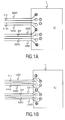
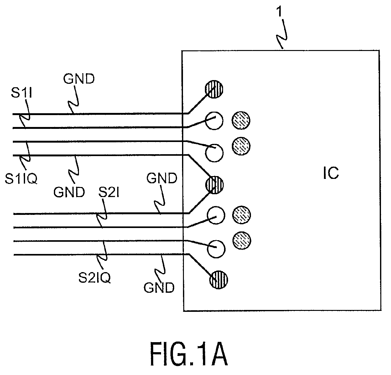
- FIG. 1 shows a preferred embodiment of an integrated circuit according to the invention, denoted IC, connected to first and second transmission lines parallel differentials, denoted S1 and S2 respectively.
- the invention is applicable in a way identical to a single transmission line.
- the presence of one or two lines S1 and S2 and connection pads associated in Figures 1 to 3, is intended to show how several lines can be connected using a device according to the invention.
- the first line S1 is breaks down into a first component, denoted S1I, and a second component, denoted S1IQ.
- the second line S2 is broken down into a first component, denoted S2I and a second component, denoted S2IQ.
- Each I or IQ component of the differential signal has in turn two separate routes including a first route or direct line carrying the useful signal to transmit and a second return channel or line brought to a voltage of reference depending on the application.
- Differential lines carry I and IQ components of signals differentials to be transmitted. They are materialized by tracks made with a material conductor traced or printed on a support of insulating material. All tracks traces form a circuit, commonly called a printed circuit or PCB, intended to interconnect integrated circuits (a single integrated circuit is shown in FIG. 1) according to a routing predetermined according to the intended application. Integrated circuits are generally located inside housings 1 made of insulating material. Connections between lines printed circuits and integrated circuits are produced by means of a set of connection pads, represented in the figure by circles. In the case where the circuit is integrated in a case of BGA type (from English Ball Gate Array) the connection pads are practically spherical and are called connection balls.
- connection pads has connections intended to receive the differential signals to be transmitted, known as signal pads and connections intended for the supply of circuits, known as supply pads.
- Food is done using two separate supply voltages, one being higher than the other and one generally corresponds to mass.
- the supply pads are therefore subjected to a voltage among two possible distinct reference voltages, one called the high reference and the other said low reference.
- Power pads are represented by circles hatched. By convention, in Figure 1, the vertical hatching corresponds to the connected studs at the low reference and the cross-hatching corresponds to the studs connected to the reference high.
- the integrated circuit According to a first configuration, called positive configuration, the low reference voltage corresponds to ground and the high reference voltage corresponds to a constant voltage positive, denoted + VCC. According to the second configuration, called negative configuration, the voltage of low reference corresponds to a negative constant voltage, noted -VCC and the voltage of high reference corresponds to the mass.
- the integrated circuits can therefore be supplied according to either of these configurations.
- the envisaged application did not generally only one reference voltage, for example ground. In this case, it is better that the return lines of the differential lines are connected to ground.
- the earth is not connected to the same pads connections, which implies that the tracing of the printed tracks can be different from a configuration to the other as shown in Figures 1A and 1B.
- FIG. 1A illustrates an exemplary embodiment of a circuit according to the invention in the positive configuration.
- FIG. 1B illustrates the same circuit according to the negative configuration.
- the signal pads represented in FIGS. 1A and 1B by unhatched circles, are located on the edge of the housing and are surrounded by the supply studs which receive constant reference voltages.
- the arrangement of the pairs of connection pads is symmetrical with respect to a plane perpendicular to the PCB plane and perpendicular to the side of the box closest to the set of connection pads considered.
- This arrangement of the studs connection is compatible with the two possible power supply configurations.
- the direct transmission lines and the signal pads to which they are connected are surrounded by earth or power, depending on the configuration used, thus forming a protective screen against possible electromagnetic interference generated by signals transmitted at high frequency.
- a first advantage is the ease of access of the signal pads.
- the signal pads are arranged at the edge of the box to allow direct access to transmission lines.
- a second advantage is the symmetry of the device.
- the connection pads are arranged on the housing of symmetrically with respect to a plane perpendicular to the plane of the integrated circuit and passing parallel to the transmission lines by a midpoint separating said transmission lines transmission. This means that the distances traveled by the signal can be the same on each complementary differential component SI and SIQ of the transmission line, with all the well-known benefits that this entails.
- a third advantage is the quality of the shielding. Each pair of transmission lines is framed to the signal pad by two clean reference lines, not noisy, which promotes good signal transmission.
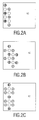
- FIG. 2 shows three other exemplary embodiments of the invention. These three examples are given for information only and are not restrictive. They can give rise to many variants without departing from the scope of the invention.
- the elements common with Figure 1 bear the same references.
- FIG. 2A illustrates a variant in which the signal pads are arranged in two rows parallel to the side of the case staggered to limit clutter.
- the power pads are arranged around and between the signal pads on the same parallel rows.
- this embodiment is not symmetrical and access to signals is less direct than in the embodiment illustrated in FIG. 1.
- FIG. 2B illustrates another alternative embodiment.
- the signal pads are always staggered in two parallel rows but the pads supply are arranged in four parallel rows and in particular between the pads signal on the two rows of signal pads, so that each signal pad is surrounded on all four sides by at least one power pad.
- This embodiment also allows limit the size of the connection pads and therefore have a larger number on the housing. It also allows you to easily add other rows or layers of connection pads to the center of the case. However, this embodiment is not symmetrical.
- FIG. 2C illustrates yet another alternative embodiment.
- the signal pads are arranged in successive pairs separated by at least one pad supply on the same row parallel to the side of the housing.
- the other power pads are arranged on either side of the row of signal pads so as to surround each pair of signal pads.
Landscapes
- Physics & Mathematics (AREA)
- Electromagnetism (AREA)
- Engineering & Computer Science (AREA)
- Microelectronics & Electronic Packaging (AREA)
- Semiconductor Integrated Circuits (AREA)
- Structure Of Printed Boards (AREA)
- Shielding Devices Or Components To Electric Or Magnetic Fields (AREA)
- Noise Elimination (AREA)
- Internal Circuitry In Semiconductor Integrated Circuit Devices (AREA)
Abstract
Description
- la figure 1 est un schéma pour illustrer un exemple de réalisation d'un circuit selon l'invention, selon deux configurations d'applications, illustrées aux figures 1A et 1B,
- la figure 2 est un schéma pour illustrer trois autres exemples de réalisation de l'invention, illustrés aux figures 2A, 2B et 2C, respectivement.
Claims (9)
- Dispositif comprenant un circuit intégré et un jeu de plots de connexion pour connecter ledit circuit intégré avec au moins une paire de lignes de transmission destinées à véhiculer des signaux électriques à destination et/ou en provenance dudit circuit intégré, le jeu de plots de connexion comprenant au moins une première paire de plots de connexion destinés à recevoir une première tension de référence, une deuxième paire de plots de connexion destinés à recevoir une deuxième tension de référence et une troisième paire de plots de connexion, dits plots de signal, destinés à être reliés à ladite paire de lignes de transmission, caractérisé en ce que lesdits plots de signal sont entourés par lesdites première et deuxième paires de plots de connexion.
- Dispositif selon la revendication 1, dans lequel ladite paire de lignes de transmission comprend deux composantes pour transmettre en parallèle des signaux électriques différentiels simultanément, chaque composante étant reliée à un plot de signal distinct.
- Dispositif selon la revendication 1 ou 2, dans lequel les première et deuxième tensions de référence correspondent à des tensions d'alimentation dudit circuit intégré, dont une tension d'alimentation, dite tension haute, est supérieure à l'autre, dite tension basse, une seule tension d'alimentation correspondant à la masse, réalisant ainsi deux possibilités de configurations d'alimentation distinctes, dites configurations positive et négative, selon que la masse correspond à la tension haute ou basse, respectivement.
- Dispositif selon la revendication 3, dans lequel la paire de lignes de transmission est associée à une paire de lignes de retour destinées à véhiculer lesdits signaux électriques en sens inverse, caractérisé en ce que la paire de plots de connexion destinée à recevoir la masse est destinée à être reliée à ladite paire de lignes de retour.
- Dispositif selon l'une des revendications 1 à 4 , dans lequel les paires de plots de connexion sont disposés symétriquement par rapport à un plan perpendiculaire au plan du circuit intégré et passant parallèlement aux lignes de transmission par un point milieu séparant lesdites lignes de transmission.
- Dispositif selon l'une des revendications 1 à 4, dans lequel le circuit intégré est intégré dans un boítier, caractérisé en ce que les plots de signal sont disposés en bordure du boítier de façon à être immédiatement accessibles par les lignes de transmission.
- Dispositif selon la revendications 6 , dans lequel le boítier est du type BGA (de l'anglais Ball Gate Array).
- Circuit imprimé comportant un support en matériau isolant pour supporter un dispositif selon l'une des revendications 1 à 7, caractérisé en ce que les lignes de transmission et les lignes de retour sont imprimées sur ledit circuit.
- Appareil de télécommunication comportant un dispositif selon l'une des revendications 1 à 8.
Applications Claiming Priority (2)
| Application Number | Priority Date | Filing Date | Title |
|---|---|---|---|
| FR0114664 | 2001-11-13 | ||
| FR0114664 | 2001-11-13 |
Publications (2)
| Publication Number | Publication Date |
|---|---|
| EP1310995A2 true EP1310995A2 (fr) | 2003-05-14 |
| EP1310995A3 EP1310995A3 (fr) | 2010-10-20 |
Family
ID=8869341
Family Applications (1)
| Application Number | Title | Priority Date | Filing Date |
|---|---|---|---|
| EP02079626A Withdrawn EP1310995A3 (fr) | 2001-11-13 | 2002-11-06 | Dispositif de blindage des lignes de transmission par la masse ou l'alimentation |
Country Status (6)
| Country | Link |
|---|---|
| US (1) | US6791165B2 (fr) |
| EP (1) | EP1310995A3 (fr) |
| JP (1) | JP4454926B2 (fr) |
| KR (1) | KR20030040071A (fr) |
| CN (1) | CN1331225C (fr) |
| TW (1) | TW200408091A (fr) |
Cited By (2)
| Publication number | Priority date | Publication date | Assignee | Title |
|---|---|---|---|---|
| WO2015146738A1 (fr) * | 2014-03-24 | 2015-10-01 | 技術研究組合光電子融合基盤技術研究所 | Structure de réseau de plots sur un substrat pour monter une puce à circuits intégrés (ic) sur le substrat et module optique ayant ladite structure de réseau de plots |
| WO2018209003A1 (fr) * | 2017-05-10 | 2018-11-15 | Qualcomm Incorporated | Connecteur pour routage différentiel |
Families Citing this family (20)
| Publication number | Priority date | Publication date | Assignee | Title |
|---|---|---|---|---|
| US6700181B1 (en) * | 2002-11-19 | 2004-03-02 | Inphi Corporation | Method and system for broadband transition from IC package to motherboard |
| US20070262448A1 (en) * | 2004-08-20 | 2007-11-15 | Tsutomu Ishino | Semiconductor Device, Power Supply Apparatus Using Same, and Electronic Device |
| US7294976B1 (en) | 2005-09-23 | 2007-11-13 | Advanced Micro Devices, Inc. | Split power supply subsystem with isolated voltage supplies to satisfy a predetermined power limit |
| JP4595823B2 (ja) * | 2006-01-24 | 2010-12-08 | 株式会社デンソー | ボールグリッドアレイ |
| JP5336700B2 (ja) * | 2006-11-30 | 2013-11-06 | ローム株式会社 | 半導体装置およびそれを用いた電子機器 |
| JP5034095B2 (ja) * | 2007-07-13 | 2012-09-26 | 株式会社リコー | プリント配線基板および電子装置 |
| US8310276B2 (en) | 2008-06-27 | 2012-11-13 | Canon Kabushiki Kaisha | Differential transmission circuit |
| JP5028357B2 (ja) * | 2008-08-07 | 2012-09-19 | キヤノン株式会社 | 差動伝送回路 |
| JP2010010492A (ja) | 2008-06-27 | 2010-01-14 | Sony Corp | 半導体装置および半導体集積回路 |
| KR100951667B1 (ko) * | 2008-08-19 | 2010-04-07 | 주식회사 하이닉스반도체 | 패드를 포함하는 반도체 메모리 장치 |
| TWI407421B (zh) | 2009-02-17 | 2013-09-01 | Au Optronics Corp | 用於驅動一液晶顯示面板之驅動裝置 |
| CN101494040B (zh) * | 2009-03-06 | 2013-05-08 | 友达光电股份有限公司 | 用于驱动一液晶显示面板的驱动装置 |
| JP5351063B2 (ja) | 2010-01-13 | 2013-11-27 | 株式会社アドバンテスト | コンタクト装置及び回路パッケージ |
| JP5416269B2 (ja) * | 2012-12-11 | 2014-02-12 | 古河電気工業株式会社 | 並列光伝送装置 |
| JP2015153808A (ja) * | 2014-02-12 | 2015-08-24 | ソニー株式会社 | 半導体チップ、および、半導体モジュール |
| JP6527420B2 (ja) * | 2015-07-31 | 2019-06-05 | ルネサスエレクトロニクス株式会社 | 半導体装置 |
| WO2018042518A1 (fr) * | 2016-08-30 | 2018-03-08 | 株式会社日立製作所 | Dispositif à semi-conducteur et carte de circuit imprimé |
| TWI684245B (zh) * | 2018-08-29 | 2020-02-01 | 財團法人工業技術研究院 | 差動訊號傳輸電路板 |
| JP7613025B2 (ja) * | 2020-09-04 | 2025-01-15 | セイコーエプソン株式会社 | 電子機器、及び半導体集積回路装置 |
| KR102961554B1 (ko) | 2021-08-27 | 2026-05-06 | 삼성전자주식회사 | 메모리 장치 및 그 동작 방법 |
Family Cites Families (19)
| Publication number | Priority date | Publication date | Assignee | Title |
|---|---|---|---|---|
| JP3014503B2 (ja) * | 1991-08-05 | 2000-02-28 | 日本特殊陶業株式会社 | 集積回路用パッケージ |
| US5714801A (en) * | 1995-03-31 | 1998-02-03 | Kabushiki Kaisha Toshiba | Semiconductor package |
| US5796170A (en) * | 1996-02-15 | 1998-08-18 | Northern Telecom Limited | Ball grid array (BGA) integrated circuit packages |
| US5686764A (en) * | 1996-03-20 | 1997-11-11 | Lsi Logic Corporation | Flip chip package with reduced number of package layers |
| GB2324649A (en) * | 1997-04-16 | 1998-10-28 | Ibm | Shielded semiconductor package |
| US6215184B1 (en) * | 1998-02-19 | 2001-04-10 | Texas Instruments Incorporated | Optimized circuit design layout for high performance ball grid array packages |
| US6057600A (en) * | 1997-11-27 | 2000-05-02 | Kyocera Corporation | Structure for mounting a high-frequency package |
| US5994766A (en) * | 1998-09-21 | 1999-11-30 | Vlsi Technology, Inc. | Flip chip circuit arrangement with redistribution layer that minimizes crosstalk |
| US6373447B1 (en) * | 1998-12-28 | 2002-04-16 | Kawasaki Steel Corporation | On-chip antenna, and systems utilizing same |
| JP2000349192A (ja) * | 1999-06-07 | 2000-12-15 | Canon Inc | 半導体集積回路およびプリント配線板 |
| US6329702B1 (en) * | 2000-07-06 | 2001-12-11 | Tyco Electronics Corporation | High frequency carrier |
| US6563299B1 (en) * | 2000-08-30 | 2003-05-13 | Micron Technology, Inc. | Apparatus for measuring parasitic capacitance and inductance of I/O leads on an electrical component using a network analyzer |
| US20020113309A1 (en) * | 2001-01-04 | 2002-08-22 | Siamak Fazelpour | Shielding of RF devices |
| JP4536942B2 (ja) * | 2001-02-09 | 2010-09-01 | 三菱電機株式会社 | 高周波用集積回路及びこれを用いた高周波回路装置 |
| JP4623850B2 (ja) * | 2001-03-27 | 2011-02-02 | 京セラ株式会社 | 高周波半導体素子収納用パッケージおよびその実装構造 |
| JP2003068928A (ja) * | 2001-08-28 | 2003-03-07 | Kyocera Corp | 高周波用配線基板の実装構造 |
| US6603193B2 (en) * | 2001-09-06 | 2003-08-05 | Silicon Bandwidth Inc. | Semiconductor package |
| US6635958B2 (en) * | 2001-12-03 | 2003-10-21 | Dover Capital Formation Group | Surface mount ceramic package |
| US20030198032A1 (en) * | 2002-04-23 | 2003-10-23 | Paul Collander | Integrated circuit assembly and method for making same |
-
2002
- 2002-11-01 TW TW091132393A patent/TW200408091A/zh unknown
- 2002-11-06 EP EP02079626A patent/EP1310995A3/fr not_active Withdrawn
- 2002-11-07 JP JP2002323857A patent/JP4454926B2/ja not_active Expired - Fee Related
- 2002-11-08 CN CNB021499233A patent/CN1331225C/zh not_active Expired - Fee Related
- 2002-11-08 US US10/291,035 patent/US6791165B2/en not_active Expired - Lifetime
- 2002-11-08 KR KR1020020069137A patent/KR20030040071A/ko not_active Withdrawn
Cited By (4)
| Publication number | Priority date | Publication date | Assignee | Title |
|---|---|---|---|---|
| WO2015146738A1 (fr) * | 2014-03-24 | 2015-10-01 | 技術研究組合光電子融合基盤技術研究所 | Structure de réseau de plots sur un substrat pour monter une puce à circuits intégrés (ic) sur le substrat et module optique ayant ladite structure de réseau de plots |
| JPWO2015146738A1 (ja) * | 2014-03-24 | 2017-04-13 | 技術研究組合光電子融合基盤技術研究所 | Icチップを基板に搭載させるための基板上のパッド・アレイ構造、並びに当該パッド・アレイ構造を有する光モジュール |
| US9775245B2 (en) | 2014-03-24 | 2017-09-26 | Photonics Electronics Technology Research Association | Pad-array structure on substrate for mounting IC chip on substrate, and optical module having said pad-array structure |
| WO2018209003A1 (fr) * | 2017-05-10 | 2018-11-15 | Qualcomm Incorporated | Connecteur pour routage différentiel |
Also Published As
| Publication number | Publication date |
|---|---|
| TW200408091A (en) | 2004-05-16 |
| EP1310995A3 (fr) | 2010-10-20 |
| KR20030040071A (ko) | 2003-05-22 |
| JP2003249904A (ja) | 2003-09-05 |
| CN1419287A (zh) | 2003-05-21 |
| US6791165B2 (en) | 2004-09-14 |
| CN1331225C (zh) | 2007-08-08 |
| US20030102536A1 (en) | 2003-06-05 |
| JP4454926B2 (ja) | 2010-04-21 |
Similar Documents
| Publication | Publication Date | Title |
|---|---|---|
| JP4454926B2 (ja) | グランド又は電源回路より伝送線をシールドするための装置 | |
| JP7095583B2 (ja) | 光送信機 | |
| FR2695272A1 (fr) | Circuit mélangeur pour des signaux de radio ou de télévision. | |
| CA1300238C (fr) | Dispositif de distribution de signaux numeriques a tres hauts debits | |
| JP6988322B2 (ja) | 光受信モジュール用パッケージ | |
| JP6448045B2 (ja) | 光電気集積回路及び光インタポーザ | |
| FR2828580A1 (fr) | Module de puissance | |
| FR2735324A1 (fr) | Carte de cablage stratifiee | |
| FR3071932B1 (fr) | Commutateurs et reseau d'interconnexion photonique integre dans une puce optoelectronique | |
| KR20150074077A (ko) | 트랜스임피던스 증폭기로부터 멀리 위치한 광-검출기 및 관련된 컴포넌트들, 회로들을 갖는 수신기 광 어셈블리들(roas), 및 방법들 | |
| EP0596568A1 (fr) | Dispositif semiconducteur comprenant un circuit amplificateur distribué monolithiquement intégré, à large bande et fort gain | |
| EP0346206A1 (fr) | Connecteur actif pour carte de circuits imprimés | |
| JP2020079850A (ja) | 光送受信器 | |
| US20090003844A1 (en) | High speed optoelectronic receiver | |
| JP2007266251A (ja) | 光半導体装置 | |
| JP2019101140A (ja) | 光変調器及びそれを用いた光送信装置 | |
| FR3074402B1 (fr) | Systeme a boucle de masse integrant un dispositif de couplage electrique agissant sur un courant parasite | |
| JP7842361B2 (ja) | 光受信器 | |
| JP3269654B2 (ja) | 光電子送受信装置 | |
| EP0606943B1 (fr) | Dispositif commutateur de signaux de télévision pour une distribution par câble | |
| KR100440431B1 (ko) | 고속 광전 모듈의 광전소자 서브마운트 | |
| EP3675606A1 (fr) | Circuit imprime permettant d'avoir un connecteur qsfp en belly-to-belly avec un connecteur qsfp-dd et systeme associe | |
| KR100699569B1 (ko) | 양방향 광송수신 모듈 패키지 | |
| FR2503503A1 (fr) | Appareil de prise de vues | |
| JP2764127B2 (ja) | 光接続集積回路 |
Legal Events
| Date | Code | Title | Description |
|---|---|---|---|
| PUAI | Public reference made under article 153(3) epc to a published international application that has entered the european phase |
Free format text: ORIGINAL CODE: 0009012 |
|
| AK | Designated contracting states |
Designated state(s): AT BE BG CH CY CZ DE DK EE ES FI FR GB GR IE IT LI LU MC NL PT SE SK TR |
|
| AX | Request for extension of the european patent |
Extension state: AL LT LV MK RO SI |
|
| RAP1 | Party data changed (applicant data changed or rights of an application transferred) |
Owner name: NXP B.V. |
|
| PUAL | Search report despatched |
Free format text: ORIGINAL CODE: 0009013 |
|
| AK | Designated contracting states |
Kind code of ref document: A3 Designated state(s): AT BE BG CH CY CZ DE DK EE ES FI FR GB GR IE IT LI LU MC NL PT SE SK TR |
|
| AX | Request for extension of the european patent |
Extension state: AL LT LV MK RO SI |
|
| 17P | Request for examination filed |
Effective date: 20110411 |
|
| AKX | Designation fees paid |
Designated state(s): AT BE BG CH CY CZ DE DK EE ES FI FR GB GR IE IT LI LU MC NL PT SE SK TR |
|
| 17Q | First examination report despatched |
Effective date: 20110825 |
|
| STAA | Information on the status of an ep patent application or granted ep patent |
Free format text: STATUS: THE APPLICATION IS DEEMED TO BE WITHDRAWN |
|
| 18D | Application deemed to be withdrawn |
Effective date: 20150922 |