EP1288862A2 - Bildauswertungsverfahren und Mikroskop - Google Patents
Bildauswertungsverfahren und Mikroskop Download PDFInfo
- Publication number
- EP1288862A2 EP1288862A2 EP02018519A EP02018519A EP1288862A2 EP 1288862 A2 EP1288862 A2 EP 1288862A2 EP 02018519 A EP02018519 A EP 02018519A EP 02018519 A EP02018519 A EP 02018519A EP 1288862 A2 EP1288862 A2 EP 1288862A2
- Authority
- EP
- European Patent Office
- Prior art keywords
- image
- resolution
- evaluation
- charged
- particle beam
- Prior art date
- Legal status (The legal status is an assumption and is not a legal conclusion. Google has not performed a legal analysis and makes no representation as to the accuracy of the status listed.)
- Granted
Links
- 238000011156 evaluation Methods 0.000 title claims abstract description 85
- 238000012935 Averaging Methods 0.000 claims abstract description 8
- 239000002245 particle Substances 0.000 claims description 36
- 238000004364 calculation method Methods 0.000 claims description 13
- 230000006870 function Effects 0.000 claims description 12
- 238000007689 inspection Methods 0.000 claims description 12
- 238000005259 measurement Methods 0.000 claims description 8
- 238000012545 processing Methods 0.000 claims description 6
- 239000011163 secondary particle Substances 0.000 claims description 6
- 238000003672 processing method Methods 0.000 claims description 4
- 238000013459 approach Methods 0.000 claims description 2
- 238000010276 construction Methods 0.000 claims description 2
- 238000012886 linear function Methods 0.000 claims 2
- 238000000034 method Methods 0.000 abstract description 26
- 238000001000 micrograph Methods 0.000 abstract description 18
- 230000000694 effects Effects 0.000 description 11
- 238000010894 electron beam technology Methods 0.000 description 10
- 238000004519 manufacturing process Methods 0.000 description 8
- 239000004065 semiconductor Substances 0.000 description 8
- 238000001878 scanning electron micrograph Methods 0.000 description 6
- 125000003821 2-(trimethylsilyl)ethoxymethyl group Chemical group [H]C([H])([H])[Si](C([H])([H])[H])(C([H])([H])[H])C([H])([H])C(OC([H])([H])[*])([H])[H] 0.000 description 5
- PCHJSUWPFVWCPO-UHFFFAOYSA-N gold Chemical compound [Au] PCHJSUWPFVWCPO-UHFFFAOYSA-N 0.000 description 5
- 239000010931 gold Substances 0.000 description 5
- 229910052737 gold Inorganic materials 0.000 description 5
- 230000003287 optical effect Effects 0.000 description 5
- 238000004626 scanning electron microscopy Methods 0.000 description 5
- 230000008030 elimination Effects 0.000 description 4
- 238000003379 elimination reaction Methods 0.000 description 4
- 230000008901 benefit Effects 0.000 description 3
- 238000012937 correction Methods 0.000 description 3
- 238000010586 diagram Methods 0.000 description 3
- 239000000758 substrate Substances 0.000 description 3
- OKTJSMMVPCPJKN-UHFFFAOYSA-N Carbon Chemical compound [C] OKTJSMMVPCPJKN-UHFFFAOYSA-N 0.000 description 2
- XUIMIQQOPSSXEZ-UHFFFAOYSA-N Silicon Chemical compound [Si] XUIMIQQOPSSXEZ-UHFFFAOYSA-N 0.000 description 2
- 238000004458 analytical method Methods 0.000 description 2
- 229910052799 carbon Inorganic materials 0.000 description 2
- 238000009826 distribution Methods 0.000 description 2
- 230000008020 evaporation Effects 0.000 description 2
- 238000001704 evaporation Methods 0.000 description 2
- 230000010354 integration Effects 0.000 description 2
- 238000010884 ion-beam technique Methods 0.000 description 2
- 230000008569 process Effects 0.000 description 2
- 238000003908 quality control method Methods 0.000 description 2
- 229910052710 silicon Inorganic materials 0.000 description 2
- 239000010703 silicon Substances 0.000 description 2
- 230000002194 synthesizing effect Effects 0.000 description 2
- 238000012546 transfer Methods 0.000 description 2
- 230000002411 adverse Effects 0.000 description 1
- 230000005540 biological transmission Effects 0.000 description 1
- 230000008859 change Effects 0.000 description 1
- 238000011109 contamination Methods 0.000 description 1
- 230000002542 deteriorative effect Effects 0.000 description 1
- 238000005530 etching Methods 0.000 description 1
- 238000012854 evaluation process Methods 0.000 description 1
- 230000005284 excitation Effects 0.000 description 1
- 230000001747 exhibiting effect Effects 0.000 description 1
- 238000010191 image analysis Methods 0.000 description 1
- 238000003754 machining Methods 0.000 description 1
- 238000005457 optimization Methods 0.000 description 1
- 230000009467 reduction Effects 0.000 description 1
- 230000003252 repetitive effect Effects 0.000 description 1
- 239000000523 sample Substances 0.000 description 1
- 238000001228 spectrum Methods 0.000 description 1
- 230000001360 synchronised effect Effects 0.000 description 1
- 239000010409 thin film Substances 0.000 description 1
- 238000012795 verification Methods 0.000 description 1
Images


Classifications
-
- H—ELECTRICITY
- H01—ELECTRIC ELEMENTS
- H01J—ELECTRIC DISCHARGE TUBES OR DISCHARGE LAMPS
- H01J37/00—Discharge tubes with provision for introducing objects or material to be exposed to the discharge, e.g. for the purpose of examination or processing thereof
- H01J37/26—Electron or ion microscopes; Electron or ion diffraction tubes
- H01J37/28—Electron or ion microscopes; Electron or ion diffraction tubes with scanning beams
-
- H—ELECTRICITY
- H01—ELECTRIC ELEMENTS
- H01J—ELECTRIC DISCHARGE TUBES OR DISCHARGE LAMPS
- H01J37/00—Discharge tubes with provision for introducing objects or material to be exposed to the discharge, e.g. for the purpose of examination or processing thereof
- H01J37/02—Details
- H01J37/22—Optical, image processing or photographic arrangements associated with the tube
- H01J37/222—Image processing arrangements associated with the tube
-
- H—ELECTRICITY
- H01—ELECTRIC ELEMENTS
- H01J—ELECTRIC DISCHARGE TUBES OR DISCHARGE LAMPS
- H01J37/00—Discharge tubes with provision for introducing objects or material to be exposed to the discharge, e.g. for the purpose of examination or processing thereof
- H01J37/26—Electron or ion microscopes; Electron or ion diffraction tubes
- H01J37/261—Details
- H01J37/263—Contrast, resolution or power of penetration
-
- H—ELECTRICITY
- H01—ELECTRIC ELEMENTS
- H01J—ELECTRIC DISCHARGE TUBES OR DISCHARGE LAMPS
- H01J2237/00—Discharge tubes exposing object to beam, e.g. for analysis treatment, etching, imaging
- H01J2237/26—Electron or ion microscopes
- H01J2237/282—Determination of microscope properties
- H01J2237/2823—Resolution
Definitions
- the present invention relates to methods for evaluating microscope images such as from scanning electron microscopes and scanning ion microscopes and relates in particular to a method for evaluating image resolution and a microscope having an evaluation function.
- the other is the FFT method as disclosed in JP-A-24640/1999 for evaluating image resolution by frequency analysis of observation image data that was subjected to two-dimensional Fourier transform (FFT).
- FFT two-dimensional Fourier transform
- the first gap method of the related art has the problem that high accuracy and repeatability of image resolution evaluation values cannot be expected because the size and shape of the gold particles to be imaged are not uniform and because the human evaluator may not be objective when visually determining the minimum gap between two particles.
- the second FFT method of the related art also has the problem that resolution is visually evaluated with a resolution determination curve plotted on a power spectrum graph for frequency analysis, so subjectivity on the part of the evaluator still cannot be eliminated.
- the present invention has the object of providing an image evaluation method for objectively determining image resolution of microscope images, and a microscope having a resolution evaluation function.
- the present invention provides an image evaluation method for evaluating image resolution, wherein the resolution in partial regions of the image is obtained over an entire area or a portion of the image, averaging is performed over an entire area or a portion of the image, and the averaged value becomes the resolution evaluation value for an entire area or a portion of the image.
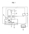
- FIG. 1 focuses a charged particle beam (electron beam) 2 emitted from a charged particle source (electron gun) 1 onto a specimen 4 by an electron lens 3 and scans the beam over the specimen 4 in any desired sequence.
- Secondary particles (secondary electrons) 5 generated from the surface of the specimen 4 by irradiation of the electron beam are detected by a secondary particle detector system 6.
- the output of the detector system 6 is input as image data to a control system 7 (control processor) having an image processing and control function.
- the specimen 4 can be moved along in any direction in the three dimensions by use of an X-Y-Z stage 8.
- the control system 7 also controls the charged particle source (electron gun) 1, the electron lens 3, the secondary particle detector system 6, X-Y-Z stage 8, and an image display device 9.
- the electron beam 2 is two-dimensionally scanned over the surface of the specimen 4 with a scanning coil (not shown in drawing).
- the signal detected with a secondary electron detector in the secondary particle detector system 6 is transferred to an image memory after being amplified by a signal amplifier in the control system 7 and is finally displayed as an image of the specimen on the image display device 9.
- the secondary signal detector may be a secondary electron or reflected electron detector, photodetector or X-ray detector.
- the address signals corresponding to the memory positions in the image memory are generated in the control system 7 or a separately installed computer, and supplied to a scanning coil after being converted into analog signals.
- the image memory has 512 x 512 pixels
- the X-direction address signal is a digital signal representing 0 to 512 repeatedly.
- the Y-direction address signal is also a digital signal representing 0 to 512 repeatedly but is incremented by 1 each time the X-direction address signal reaches 512 from 0. These digital signals are converted into analog signals.
- the addresses in the image memory correspond to addresses of deflection signals for scanning the electron beam
- a two-dimensional image in the electron beam deflection range determined by the scanning coil is stored in the image memory.
- the signals in the image memory can be sequentially read out in time series by a readout address generator circuit synchronized with a readout clock.
- the signals that were read out according to each address are converted into an analog signal and input to the image display device 9 as a brightness-modulated signal.
- the image memory has a function for storing images (image data) while superimposing (synthesizing) them in order to improve the signal-to-noise ratio.
- images image data
- a final image is created by synthesizing images that were formed by one or more X-Y scans.
- the number of images (frame integration count) for creating one complete image can be set arbitrarily to an optimum value in view of factors such as the efficiency of generating secondary electrons.
- Another final image can also be created as needed by further superimposing images that were created by integrating multiple image frames. When or after the desired number of images has been stored, blanking may be performed with the primary electron beam to stop the input of information to the image memory.
- a sequence may be made so that the first image frame is deleted when the ninth image frame is input so that there are always 8 image frames.
- Weighted averaging can also be performed, for example, by adding the product of the image integrated in the image memory times (x) 7/8, to the ninth image when the ninth image is input.
- the control system 7 has an input device (not shown in drawing) that specifies the image acquisition conditions (scanning speed, number of images to be integrated), field-of-view correction method and how images should be output or saved.
- the control system 7 incorporates a memory medium (not shown in drawing) for storing various types of data.
- This embodiment of the present invention also provides a function that forms a line profile based on the detected secondary electrons or reflected electrons.
- a line profile should be formed based on the quantity of detected electrons when a specimen is scanned one-dimensionally or two-dimensionally with the primary electron beam, or based on the brightness information of the specimen image.
- a line profile obtained this way will be used, for example, to measure the dimensions of patterns formed on a semiconductor wafer.
- the schematic diagram in FIG. 1 was explained with the control system 7 as an in integral or semi-integral unit of the scanning electron microscope.
- the embodiment of the present invention is not limited by this example and may have an external control processor installed separately from the scanning electron microscope to perform the processing explained below. This case will require transfer media for sending the signals detected with the secondary signal detector to the control processor or sending the signals from the control processor to the electron lens and deflector of the scanning electron microscope, and also an input/output terminal for inputting and outputting the signals sent by way of the transfer media.
- this embodiment of the present invention also provides a function that for example, allows storing the observation conditions (measurement points, optical conditions for electron scanning microscope, etc.) in advance as a guide to help assist in viewing multiple points on a semiconductor wafer. Measurement and observation can easily be performed according to the contents of this guide.
- a program intended to perform the processing explained below may be stored in the memory medium and executed with a control processor having an image memory and supplying signals necessary for the scanning electron microscope.
- the following embodiment of the present invention may be established as a program invention used for charged-particle beam equipment such as scanning electron microscopes with an image processor.
- a specimen is placed on stage 8 of this embodiment for evaluating image resolution as explained below.
- FIGS. 2A and 2B show SEM images of typical gold particle specimens. These are digital images consisting of 512 x 512 pixels. Image resolution is calculated by the evaluation algorithm explained below. The concept for evaluating image resolution is shown in FIG. 8 along with the gap resolution evaluation method, and the flow chart for calculating image resolution is shown in FIG. 9. A detailed description is given in the following embodiments.
- a microscope image is treated as an image of a three-dimensional object viewed from one direction, and the gradient and curvature of the object surface at each pixel point P are first obtained.
- the hypothetical shortest distance required for the object to be distinguished from the surrounding area, or in other words, the local resolution is calculated from the gradient and the minimum contrast needed to recognize the object.
- the weighted harmonic mean of the local resolution is then calculated over the entire image, and the mean value is viewed as a typical resolution of the image.
- a specific example for calculating image resolution is explained below using the flow chart shown in FIG. 9.
- a microscope image is treated as an image of a three-dimensional object viewed in one direction and the geometrical features such as the gradient and radius of curvature of the object shape are calculated by range image analysis.
- the image is a digital image consisting of n x n pixels.
- the position of a pixel at an arbitrary point on the image is considered as (x, y), and the density at the pixel as "z".
- a quadratic equation is used as a multi-degree equation for approximating with a curved surface, as expressed in the quadratic equation (Eq. 1) below.
- z(x, y) ax 2 + by 2 + cxy + dx + ey + f
- the coefficients "a” to "f” are determined so that the sum-square value of the fitting error is minimal.
- the gradient g(x, y; ⁇ ) [ ⁇ is azimuth angle of gradient] of the local surface can be found by the following geometrical calculation (Eq. 2).
- g(x, y; ⁇ ) ⁇ ( ⁇ z/ ⁇ x) 2 + ( ⁇ z/ ⁇ y) 2 ⁇ 1/2
- ⁇ arctan ⁇ ( ⁇ z/ ⁇ y)/( ⁇ z/ ⁇ x) ⁇
- the radius of curvature, Rc can also be similarly computed. Applying this approximated curved surface is also effective in eliminating the noise of the image. More specifically, by clipping out a part of an image containing noise and approximating it with a curved surface or plane, the noise can be partially eliminated, allowing calculation of the gradient with fewer adverse effects from noise.
- the 3 x 3 pixel size was used as the local region size for images having less noise and containing a large quantity of frequency components having a period of less than 5 pixels on the image pattern because the gradient calculation accuracy is better.
- a plane display functional equation is linear
- the calculation time becomes shorter but the noise elimination effect is poor compared to cases using the curved surface for the quadratic equation display.
- the image resolution R over the entire image is obtained by finding the geometric mean of this azimuth image resolution R( ⁇ i ) by using the whole azimuth angle.
- the image resolution calculated this way is not greatly affected even, for example, if unexpected noise intrudes into a portion of the microscope image.
- ⁇ C is the threshold contrast needed to discern a gap on the object shape that corresponds to the resolution, and is proportional to the maximum amplitude of the expected density value E ⁇ z ⁇ calculated from Eq. 1.
- Kc the proportional coefficient
- ⁇ C Kc ⁇ [E ⁇ z(max) ⁇ -E ⁇ z(min) ⁇ ]
- the local weight Wp can be considered as the gradient g only (Eq. 6a) or the product (Eq. 6b) of g times [E ⁇ z(x, y) ⁇ - E ⁇ z(min) ⁇ ].
- the latter is used when evaluating an image in which the gradient, g, is large and more attention should be paid to bright portions. This greatly relieves the effects of brightness on the resolution when brightness is changed.
- Wp(x, y)
- the standard deviation ⁇ of density (corresponding to image noise) which is a parameter for evaluating image quality can also be calculated by using the local noise ⁇ p .
- ⁇ p ⁇ 1/m ⁇ [z(x, y)-E ⁇ z(x, y) ⁇ ] 2 ⁇ 1/2
- FIGS. 2A and 2B Shown in FIG. 2A and FIG. 2B are images (512 x 512 pixels) of a specimen prepared for resolution evaluation, photographed with an SEM under different optical conditions. Image resolution Rcg by the present evaluation method and image resolution Rgap by the gap method of the related art are shown by the resolution ratio between the conditions A and B, along with evaluation errors caused by multiple human evaluators.
- the R(b)/R(a) ratio is larger than 1, but the gap method of the related art shows an error due to multiple evaluators, which is as large as ⁇ 50%. However, the error occurring in the present evaluation method is 0 as long as the same image data is used.
- the resolution evaluation algorithm stated above determines all parameters required for calculation by using only the information possessed by the image.
- the present evaluation method uses an algorithm that is not vulnerable to subjective impressions of human evaluators and has the following advantages:
- advantage (1) allows objective comparison of image resolution between microscopes of the same type and is very helpful to the users when selecting the microscope model.
- the present embodiment was explained as an example for obtaining image resolution over the entire specimen image, but preferred embodiments are not limited to it.
- Resolution in a specific region of the specimen image (smaller than the entire image but larger than a local region used for calculating the local resolution Rp) may also be calculated.
- an image region selecting device (pointing device, etc.) not shown in the drawing may be connected to the control system 7 to select any desired size at any position on the image, so that image resolution in a region corresponding to the selected image is computed.
- This method eliminates background information not directly relating to the measurement object and acquires actual image resolution in the region to be measured.
- the throughput for calculating image resolution can be improved since the calculation is performed only on a specific region.
- a scanning electron microscope (SEM) utilizing the present image evaluation method is explained below.
- the scanning electron microscope is just one example, so the present image evaluation method can be applied to most inspection devices in which images must be accurately evaluated.
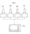
- multiple SEMs 701 to 704 are connected by a network to the master computer 705 for measuring and controlling the length of semiconductor device patterns.
- Each SEM has an image resolution computing function based on the above image resolution evaluation method, which is installed in the computer of the SEM control system. Self-evaluation of image resolution can be implemented by an instruction from the equipment operator. The resolution evaluation value appears on the monitor that also displays the microscope image.
- image resolution of each SEM is periodically evaluated by using the specimen for image resolution evaluation, displayed and recorded, along with the information on changes in the evaluation value.
- These periodically evaluated resolution values are stored in the master computer 705 where the data is collectively managed together with the information from other SEMs. If an image resolution evaluation value falls outside the allowable range or value, the operator is informed of the error on that microscope and master computer.
- the master computer 705 has an image display monitor and an image processor as explained earlier. The display monitor shows that the image resolution evaluation value is outside the allowable range or value. As specific display formats, information on changes in evaluation values on multiple SEMs may be graphically represented while distinguishing the allowable range from the area outside it.
- illustrations of multiple SEM models may be displayed on the monitor as shown in FIG. 7 and the illustration of the model on the display may start flashing if its evaluation value falls outside the allowable range or value.
- Using these display formats prevents the measurement accuracy from deteriorating even if a measurement error occurs due to a differential occurring between microscopes (instrumental error).
- the output image from an inspection device indicates a resolution evaluation value outside the allowable range, the error is displayed or stored in memory so that the instrumental error between each inspection device can be controlled while maintaining high resolution.
- a command for adjusting the optical system which is one inspection parameter is issued by an instruction from the operator or from the program installed in the control system.
- the lens system is then controlled by the signal based on the evaluation value through the control system of the microscope, so that the image resolution is set within the specified allowable range.
- Information on the adjustment process is stored in the SEM that caused the error and also sent to the master computer.
- each SEM evaluated its own image resolution; however the master computer for system control may evaluate the resolution of images sent from each SEM and send the evaluation value signal back to each SEM. Based on this evaluation value signal, each SEM controls the lens system through the control system of the microscope in the same way as described above in order to set the image resolution within the specified allowable range.
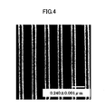
- FIG. 4 shows an SEM image of this calibration specimen.
- the pitch dimension of the grid pattern formed on a silicon substrate is an extremely accurate 0.240 ⁇ 0.001 ⁇ m.
- the resolution evaluation value R is convenient during actual use because it is displayed in units of actual dimensions (length) that do not depend on the viewing magnification.
- pixel unit display on the other hand, a specified number of pixels is allocated to the image resolution value, making it convenient to directly calculate the optimum viewing magnification.
- length units are usually used, but the pixel unit or both units can also be simultaneously displayed at the discretion of the equipment operator. By presetting the number of pixels to be allocated for image resolution, the viewing magnification can be automatically set for various specimens.
- Image resolution and signal-to-noise ratio are parameters used for evaluating image quality of a microscope images.
- C ⁇ log 2 (1+SNR) ⁇ /R 2
- the image can therefore now be evaluated in terms of image resolution, noise, and image quality.
- a threshold level for at least one of these evaluation parameters to determine whether the image is a pass (acceptable) or a fail (reject)
- the image that was obtained can be judged as acceptable or a reject based on these pass/fail parameters as well as each evaluation value.
- the image display device displays different messages according to the evaluation value and pass/fail results (for example, whether the threshold level is exceeded, to what extent the threshold level was exceeded, etc.).
- the messages to be displayed can also be selected by the equipment operator.
- the messages may be stored in the control processor memory for readout later on.
- the viewing magnification accuracy (or error) is discussed next.
- the image resolution evaluation value (unit: ⁇ m) of a microscope image taken with a dimensional calibration specimen under a particular viewing magnification is considered as R, the absolute pitch dimension of the dimensional calibration specimen as L, and the error as ⁇ x (units: ⁇ m).
- a repetitive pattern having a square-wave cross section is fabricated by silicon anisotropic etching. Each square-wave edge sharply rises perpendicular to the specimen surface.
- the viewing magnification is calibrated while measuring the pitch dimension at multiple points (about 10 to 20 points) at a magnification of 5 to 100,000, so that the average is 0.240 ⁇ m.
- the scan area of the electron beam is changed so that the measured average value approaches 0.240 ⁇ m.
- the pitch dimensions of the pattern itself have an error of a few nanometers so the measurements made at these multiple points are averaged to reduce the error.
- FIG. 5 shows typical graphical changes in the image resolution over one month, displayed on the image display monitor of SEM equipment A and B.
- the figure clearly shows that image resolutions on both units of equipment are held within the range between 3.2 and 3.8. If the resolution deviates from this range, the equipment should be serviced.
- This graph also proves that due to an instrument error the resolution of equipment B is 0.1 better than equipment A, even though the image resolutions of both pieces of equipment are within the allowable range. Based on this instrument error, a coefficient for correcting the instrumental error between the two units of equipment is found and used to correct the measurement length value. As a result, semiconductor device production can now be controlled while the instrument error between the microscopes is minimized.
- FIGS. 6A and 6B show an example of evaluation of astigmatic images using azimuth resolution.
- FIG. 6A shows microscope images of gold particles with correction parameter s. p. values at 0, 40 and 80 hours on the astigmatic image control system installed in the microscope control system 7.
- Azimuth image resolutions at this point are plotted on a polar coordinate in FIG. 6B.
- These changes indicate the extent of image blur in FIG. 6A.
- This image blur corresponds to the beam spread in the microscope.
- a microscope capable of automatically performing focus adjustment and astigmatic correction with high accuracy can be achieved by installing in the computer in the control system 7, a program combining the azimuth image resolution evaluation method with the optimization method to minimize evaluation values in all azimuth directions.
- the image resolution evaluation method of the present invention can also be used in equipment utilizing microscope images for beam positioning and setting the beam irradiation area, for example of charged-particle beam systems such as focused ion beam machining systems, electron beam diagnostic equipment, electron beam exposure systems. Therefore, the "microscopes” mentioned here include “charged-particle beam systems” utilizing microscope images.
- This technique is also very effective as an image processing method for reducing image noise.
- the density distribution after image processing is definitely the E ⁇ z(x, y) ⁇ distribution of Eq. 7.
- FIGS. 3A and 3B show the image processing effects on SEM images of a resolution standard specimen.
- FIG. 3A is the original image and
- FIG. 3B is the processed image.
- the image of FIG. 3B appears smooth because of the noise elimination effect.
- the present invention can be applied not only to SEM and SIM but also to any microscope using the gap method and FFT method of the related art as the image resolution evaluation method, for example, optical microscopes, and scanning probe microscopes.
- the image processing method of the present invention has the effect of eliminating noise on all microscope images as well as SEM and SIM.
- the microscope image resolution evaluation process of the present invention is further not susceptible to the subjective impressions of the evaluators, so image resolution evaluation values can be obtained with high reliability and repeatability.
- optical characteristics are precisely adjusted by making use of the evaluation value signal so that the desired image resolution, magnification, image noise and image quality can be maintained and controlled with a high degree of accuracy.
- the present invention when the present invention is applied to multiple microscopes used for quality control in semiconductor device production, the differential (instrumental error) in image resolution between each microscope and changes in resolution over time can be accurately controlled, making it possible to minimize variations or irregularities in device quality during the device manufacturing process.
Landscapes
- Chemical & Material Sciences (AREA)
- Analytical Chemistry (AREA)
- Engineering & Computer Science (AREA)
- Computer Vision & Pattern Recognition (AREA)
- Length-Measuring Devices Using Wave Or Particle Radiation (AREA)
- Analysing Materials By The Use Of Radiation (AREA)
- Electron Sources, Ion Sources (AREA)
- Investigating Or Analysing Materials By Optical Means (AREA)
Priority Applications (2)
| Application Number | Priority Date | Filing Date | Title |
|---|---|---|---|
| EP05010530A EP1566766B1 (de) | 2001-08-24 | 2002-08-16 | Bildauswertungsverfahren und Mikroskop |
| EP08014779.6A EP1993074B1 (de) | 2001-08-24 | 2002-08-16 | Bildauswertungsverfahren und Mikroskop |
Applications Claiming Priority (4)
| Application Number | Priority Date | Filing Date | Title |
|---|---|---|---|
| JP2001253752 | 2001-08-24 | ||
| JP2001253752 | 2001-08-24 | ||
| JP2002062817A JP4263416B2 (ja) | 2001-08-24 | 2002-03-08 | 荷電粒子顕微鏡評価システム |
| JP2002062817 | 2002-03-08 |
Related Child Applications (2)
| Application Number | Title | Priority Date | Filing Date |
|---|---|---|---|
| EP05010530A Division EP1566766B1 (de) | 2001-08-24 | 2002-08-16 | Bildauswertungsverfahren und Mikroskop |
| EP08014779.6A Division EP1993074B1 (de) | 2001-08-24 | 2002-08-16 | Bildauswertungsverfahren und Mikroskop |
Publications (3)
| Publication Number | Publication Date |
|---|---|
| EP1288862A2 true EP1288862A2 (de) | 2003-03-05 |
| EP1288862A3 EP1288862A3 (de) | 2004-04-21 |
| EP1288862B1 EP1288862B1 (de) | 2008-10-15 |
Family
ID=26620904
Family Applications (3)
| Application Number | Title | Priority Date | Filing Date |
|---|---|---|---|
| EP08014779.6A Expired - Lifetime EP1993074B1 (de) | 2001-08-24 | 2002-08-16 | Bildauswertungsverfahren und Mikroskop |
| EP02018519A Expired - Lifetime EP1288862B1 (de) | 2001-08-24 | 2002-08-16 | Bildauswertungsverfahren und Mikroskop |
| EP05010530A Expired - Lifetime EP1566766B1 (de) | 2001-08-24 | 2002-08-16 | Bildauswertungsverfahren und Mikroskop |
Family Applications Before (1)
| Application Number | Title | Priority Date | Filing Date |
|---|---|---|---|
| EP08014779.6A Expired - Lifetime EP1993074B1 (de) | 2001-08-24 | 2002-08-16 | Bildauswertungsverfahren und Mikroskop |
Family Applications After (1)
| Application Number | Title | Priority Date | Filing Date |
|---|---|---|---|
| EP05010530A Expired - Lifetime EP1566766B1 (de) | 2001-08-24 | 2002-08-16 | Bildauswertungsverfahren und Mikroskop |
Country Status (4)
| Country | Link |
|---|---|
| US (3) | US7236651B2 (de) |
| EP (3) | EP1993074B1 (de) |
| JP (1) | JP4263416B2 (de) |
| DE (2) | DE60229337D1 (de) |
Cited By (1)
| Publication number | Priority date | Publication date | Assignee | Title |
|---|---|---|---|---|
| EP2433170A1 (de) * | 2009-05-22 | 2012-03-28 | Leica Microsystems CMS GmbH | System und verfahren zum computergestützten durchführen mindestens eines tests bei einem scanmikroskop |
Families Citing this family (37)
| Publication number | Priority date | Publication date | Assignee | Title |
|---|---|---|---|---|
| DE10208289C1 (de) * | 2002-02-26 | 2003-02-27 | Koenig & Bauer Ag | Elektronischer Bildsensor und ein Verfahren zur Auswertung |
| JP3998556B2 (ja) * | 2002-10-17 | 2007-10-31 | 株式会社東研 | 高分解能x線顕微検査装置 |
| JP4012813B2 (ja) * | 2002-11-27 | 2007-11-21 | 株式会社日立ハイテクノロジーズ | 透過型電子顕微鏡及び試料観察方法 |
| JP4287671B2 (ja) * | 2003-02-19 | 2009-07-01 | 株式会社日立ハイテクノロジーズ | 測長用標準部材およびその作製方法、並びにそれを用いた電子ビーム測長装置 |
| US7539340B2 (en) * | 2003-04-25 | 2009-05-26 | Topcon Corporation | Apparatus and method for three-dimensional coordinate measurement |
| US7574016B2 (en) * | 2003-06-26 | 2009-08-11 | Fotonation Vision Limited | Digital image processing using face detection information |
| US7565030B2 (en) * | 2003-06-26 | 2009-07-21 | Fotonation Vision Limited | Detecting orientation of digital images using face detection information |
| JP4253539B2 (ja) * | 2003-07-16 | 2009-04-15 | 日本電子株式会社 | 収差制御装置を備えた荷電粒子ビーム装置 |
| US6937337B2 (en) * | 2003-11-19 | 2005-08-30 | International Business Machines Corporation | Overlay target and measurement method using reference and sub-grids |
| US7218703B2 (en) * | 2003-11-21 | 2007-05-15 | Tohken Co., Ltd. | X-ray microscopic inspection apparatus |
| JP4500099B2 (ja) * | 2004-05-06 | 2010-07-14 | 株式会社日立ハイテクノロジーズ | 電子顕微鏡装置システム及び電子顕微鏡装置システムを用いた寸法計測方法 |
| JP4628076B2 (ja) * | 2004-10-14 | 2011-02-09 | 日本電子株式会社 | 収差補正方法及び収差補正装置 |
| JP4664041B2 (ja) | 2004-10-27 | 2011-04-06 | 株式会社日立ハイテクノロジーズ | 荷電粒子ビーム装置及び試料作製方法 |
| JP4464857B2 (ja) * | 2005-04-05 | 2010-05-19 | 株式会社日立ハイテクノロジーズ | 荷電粒子線装置 |
| JP4755441B2 (ja) * | 2005-04-25 | 2011-08-24 | 株式会社日立製作所 | 設計支援方法及びシステム |
| JP4621098B2 (ja) * | 2005-09-14 | 2011-01-26 | 株式会社日立ハイテクノロジーズ | 走査型電子顕微鏡および画像信号処理方法 |
| JP2007218711A (ja) | 2006-02-16 | 2007-08-30 | Hitachi High-Technologies Corp | 電子顕微鏡装置を用いた計測対象パターンの計測方法 |
| JP4789260B2 (ja) * | 2006-08-23 | 2011-10-12 | エスアイアイ・ナノテクノロジー株式会社 | 荷電粒子ビーム装置及びアパーチャの軸調整方法 |
| JP5034570B2 (ja) * | 2007-03-09 | 2012-09-26 | 凸版印刷株式会社 | 走査型電子顕微鏡装置の評価方法及び評価装置 |
| JP4629118B2 (ja) * | 2008-03-03 | 2011-02-09 | 株式会社日立ハイテクノロジーズ | 欠陥検査装置およびこの欠陥検査装置に用いるパラメータ調整方法。 |
| JP5164754B2 (ja) * | 2008-09-08 | 2013-03-21 | 株式会社日立ハイテクノロジーズ | 走査型荷電粒子顕微鏡装置及び走査型荷電粒子顕微鏡装置で取得した画像の処理方法 |
| JP5396061B2 (ja) | 2008-10-24 | 2014-01-22 | 株式会社日立ハイテクノロジーズ | 回路パターン検査装置,回路パターン検査装置を含む管理システム、および回路パターンの検査方法 |
| JP5386502B2 (ja) * | 2008-11-05 | 2014-01-15 | 株式会社日立ハイテクノロジーズ | パターン寸法計測方法及びそれを用いた走査電子顕微鏡 |
| KR101243422B1 (ko) | 2009-01-22 | 2013-03-13 | 가부시키가이샤 히다치 하이테크놀로지즈 | 전자 현미경 |
| JP5178558B2 (ja) | 2009-02-03 | 2013-04-10 | 株式会社日立ハイテクノロジーズ | 荷電粒子線の光軸調整方法、及び荷電粒子線装置 |
| WO2011016208A1 (ja) * | 2009-08-07 | 2011-02-10 | 株式会社日立ハイテクノロジーズ | 走査型電子顕微鏡及び試料観察方法 |
| JP5292326B2 (ja) * | 2010-01-29 | 2013-09-18 | 株式会社日立ハイテクノロジーズ | 標準試料作成方法、および標準試料 |
| JP5596141B2 (ja) | 2010-05-27 | 2014-09-24 | 株式会社日立ハイテクノロジーズ | 画像処理装置、荷電粒子線装置、荷電粒子線装置調整用試料、およびその製造方法 |
| US9019417B2 (en) * | 2010-06-09 | 2015-04-28 | Mitsubishi Electric Corporation | Imaging system, imaging device and display device utilizing imaging conditions alterable according to display conditions |
| US8958898B2 (en) * | 2011-11-07 | 2015-02-17 | Nalco Company | Method and apparatus to monitor and control sheet characteristics on a creping process |
| US9070306B2 (en) * | 2012-11-02 | 2015-06-30 | Digital Surgicals Pte. Ltd. | Apparatus, method and system for microsurgical suture training |
| CN104406519A (zh) * | 2014-11-25 | 2015-03-11 | 深圳市计量质量检测研究院 | 一种放大倍率数字化测量方法和装置 |
| JP2019109960A (ja) * | 2016-03-15 | 2019-07-04 | 株式会社日立ハイテクノロジーズ | 荷電粒子ビームの評価方法、荷電粒子ビームの評価のためのコンピュータープログラム、及び荷電粒子ビームの評価装置 |
| CN108054072B (zh) * | 2017-09-07 | 2021-03-26 | 深圳市善时仪器有限公司 | 一种台式电子扫描显微镜 |
| JP7344390B6 (ja) * | 2020-07-16 | 2024-02-21 | 株式会社日立ハイテク | 補正係数計算装置、補正係数計算方法、補正係数計算プログラム |
| CN111986082B (zh) * | 2020-07-22 | 2022-06-21 | 中国西安卫星测控中心 | 一种自适应图像处理分辨率评价方法 |
| JP7437262B2 (ja) | 2020-07-31 | 2024-02-22 | 株式会社日立ハイテク | 荷電粒子線装置および電気ノイズの計測方法 |
Citations (3)
| Publication number | Priority date | Publication date | Assignee | Title |
|---|---|---|---|---|
| EP0877409A2 (de) * | 1997-05-08 | 1998-11-11 | Hitachi, Ltd. | Verfahren zur Schätzung des Auflösungsvermögens und Probe für Elektronenmikroskop |
| JPH11224640A (ja) * | 1998-02-10 | 1999-08-17 | Hitachi Ltd | 電子顕微鏡およびその分解能評価方法並びにそれを用いた半導体製造方法 |
| EP1081742A2 (de) * | 1999-09-03 | 2001-03-07 | Applied Materials, Inc. | Verfahren zur Auswertung eines Ladungsträgerstrahls |
Family Cites Families (13)
| Publication number | Priority date | Publication date | Assignee | Title |
|---|---|---|---|---|
| US4742558A (en) * | 1984-02-14 | 1988-05-03 | Nippon Telegraph & Telephone Public Corporation | Image information retrieval/display apparatus |
| JPH0545265A (ja) | 1991-08-12 | 1993-02-23 | Jeol Ltd | 走査電子顕微鏡の性能評価用試料及びその製作方法 |
| US5160931A (en) * | 1991-09-19 | 1992-11-03 | Environmental Research Institute Of Michigan | Interferometric synthetic aperture detection of sparse non-surface objects |
| JP3488745B2 (ja) | 1994-07-20 | 2004-01-19 | 独立行政法人産業技術総合研究所 | 寸法校正試料搭載ステ−ジ、及び寸法校正試料 |
| DE19644314A1 (de) * | 1995-11-23 | 1997-05-28 | Siemens Ag | Therapiegerät mit einer Quelle akustischer Wellen |
| AUPN727195A0 (en) * | 1995-12-21 | 1996-01-18 | Canon Kabushiki Kaisha | Motion detection method and apparatus |
| US6259960B1 (en) * | 1996-11-01 | 2001-07-10 | Joel Ltd. | Part-inspecting system |
| JPH10258547A (ja) * | 1997-03-19 | 1998-09-29 | Konica Corp | 画像記録装置 |
| JPH11257939A (ja) | 1998-03-12 | 1999-09-24 | Toshiba Corp | パターン寸法測定方法 |
| JP4235284B2 (ja) | 1998-08-25 | 2009-03-11 | 株式会社日立製作所 | パターン検査装置およびその方法 |
| JP3748172B2 (ja) * | 1998-12-09 | 2006-02-22 | 富士通株式会社 | 画像処理装置 |
| JP2004537142A (ja) * | 2001-07-26 | 2004-12-09 | コーニンクレッカ フィリップス エレクトロニクス エヌ ヴィ | 走査型電子顕微鏡の性能を測定する方法 |
| US7149369B2 (en) * | 2002-04-23 | 2006-12-12 | Hewlett-Packard Development Company, L.P. | Method and system for image scaling |
-
2002
- 2002-03-08 JP JP2002062817A patent/JP4263416B2/ja not_active Expired - Fee Related
- 2002-08-16 EP EP08014779.6A patent/EP1993074B1/de not_active Expired - Lifetime
- 2002-08-16 DE DE60229337T patent/DE60229337D1/de not_active Expired - Lifetime
- 2002-08-16 EP EP02018519A patent/EP1288862B1/de not_active Expired - Lifetime
- 2002-08-16 US US10/219,765 patent/US7236651B2/en not_active Expired - Fee Related
- 2002-08-16 DE DE60229448T patent/DE60229448D1/de not_active Expired - Lifetime
- 2002-08-16 EP EP05010530A patent/EP1566766B1/de not_active Expired - Lifetime
-
2005
- 2005-05-09 US US11/124,252 patent/US7340111B2/en not_active Expired - Fee Related
-
2007
- 2007-05-21 US US11/802,262 patent/US7805023B2/en not_active Expired - Fee Related
Patent Citations (3)
| Publication number | Priority date | Publication date | Assignee | Title |
|---|---|---|---|---|
| EP0877409A2 (de) * | 1997-05-08 | 1998-11-11 | Hitachi, Ltd. | Verfahren zur Schätzung des Auflösungsvermögens und Probe für Elektronenmikroskop |
| JPH11224640A (ja) * | 1998-02-10 | 1999-08-17 | Hitachi Ltd | 電子顕微鏡およびその分解能評価方法並びにそれを用いた半導体製造方法 |
| EP1081742A2 (de) * | 1999-09-03 | 2001-03-07 | Applied Materials, Inc. | Verfahren zur Auswertung eines Ladungsträgerstrahls |
Non-Patent Citations (2)
| Title |
|---|
| FANGET G L ET AL: "SURVEY OF SCANNING ELECTRON MICROSCOPES USING QUANTITATIVE RESOLUTION EVALUATION" PROCEEDINGS OF THE SPIE, SPIE, BELLINGHAM, VA, US, vol. 3050, 10 March 1997 (1997-03-10), pages 80-92, XP002054303 ISSN: 0277-786X * |
| PATENT ABSTRACTS OF JAPAN vol. 1999, no. 13, 30 November 1999 (1999-11-30) & JP 11 224640 A (HITACHI LTD), 17 August 1999 (1999-08-17) * |
Cited By (2)
| Publication number | Priority date | Publication date | Assignee | Title |
|---|---|---|---|---|
| EP2433170A1 (de) * | 2009-05-22 | 2012-03-28 | Leica Microsystems CMS GmbH | System und verfahren zum computergestützten durchführen mindestens eines tests bei einem scanmikroskop |
| US9599804B2 (en) | 2009-05-22 | 2017-03-21 | Leica Microsystems Cms Gmbh | System and method for computer-controlled execution of at least one test in a scanning microscope |
Also Published As
| Publication number | Publication date |
|---|---|
| EP1993074B1 (de) | 2013-11-06 |
| US7236651B2 (en) | 2007-06-26 |
| EP1993074A1 (de) | 2008-11-19 |
| EP1288862B1 (de) | 2008-10-15 |
| US7340111B2 (en) | 2008-03-04 |
| US7805023B2 (en) | 2010-09-28 |
| US20070280559A1 (en) | 2007-12-06 |
| DE60229448D1 (de) | 2008-11-27 |
| DE60229337D1 (de) | 2008-11-27 |
| EP1566766B1 (de) | 2008-10-15 |
| US20050199811A1 (en) | 2005-09-15 |
| EP1288862A3 (de) | 2004-04-21 |
| US20030039386A1 (en) | 2003-02-27 |
| JP2003142021A (ja) | 2003-05-16 |
| EP1566766A1 (de) | 2005-08-24 |
| JP4263416B2 (ja) | 2009-05-13 |
Similar Documents
| Publication | Publication Date | Title |
|---|---|---|
| US7340111B2 (en) | Image evaluation method and microscope | |
| US7372051B2 (en) | Electric charged particle beam microscopy, electric charged particle beam microscope, critical dimension measurement and critical dimension measurement system | |
| US6538249B1 (en) | Image-formation apparatus using charged particle beams under various focus conditions | |
| JP4069545B2 (ja) | 電子顕微方法及びそれを用いた電子顕微鏡並び生体試料検査方法及び生体検査装置 | |
| US7655906B2 (en) | Method and apparatus for scanning and measurement by electron beam | |
| US8080789B2 (en) | Sample dimension measuring method and scanning electron microscope | |
| JP4801518B2 (ja) | 荷電粒子線顕微方法および荷電粒子線装置 | |
| US20060284088A1 (en) | Focus correction method for inspection of circuit patterns | |
| US20030006371A1 (en) | Charged-particle beam apparatus and method for automatically correcting astigmatism of charged-particle beam apparatus | |
| JP3424512B2 (ja) | 粒子ビーム検査装置および検査方法並びに粒子ビーム応用装置 | |
| US8214166B2 (en) | Method and its system for calibrating measured data between different measuring tools | |
| JP4500099B2 (ja) | 電子顕微鏡装置システム及び電子顕微鏡装置システムを用いた寸法計測方法 | |
| JP4791333B2 (ja) | パターン寸法計測方法及び走査型透過荷電粒子顕微鏡 | |
| JP4709785B2 (ja) | 荷電粒子線顕微鏡、画像分解能評価用計算機、及び像分解能評価方法 | |
| JP4548432B2 (ja) | 電子顕微方法及びそれを用いた電子顕微鏡並び生体試料検査方法及び生体検査装置 | |
| JPH11224640A (ja) | 電子顕微鏡およびその分解能評価方法並びにそれを用いた半導体製造方法 | |
| JP4274146B2 (ja) | 像評価方法及び顕微鏡 | |
| JP2000311645A (ja) | 電子顕微鏡 | |
| JP4730319B2 (ja) | 像評価方法及び顕微鏡 | |
| JP4069785B2 (ja) | 電子顕微方法及びそれを用いた電子顕微鏡並び生体試料検査方法及び生体検査装置 | |
| Holburn et al. | Topographical analysis in the SEM using an automatic focusing technique |
Legal Events
| Date | Code | Title | Description |
|---|---|---|---|
| PUAI | Public reference made under article 153(3) epc to a published international application that has entered the european phase |
Free format text: ORIGINAL CODE: 0009012 |
|
| AK | Designated contracting states |
Kind code of ref document: A2 Designated state(s): AT BE BG CH CY CZ DE DK EE ES FI FR GB GR IE IT LI LU MC NL PT SE SK TR |
|
| AX | Request for extension of the european patent |
Extension state: AL LT LV MK RO SI |
|
| PUAL | Search report despatched |
Free format text: ORIGINAL CODE: 0009013 |
|
| AK | Designated contracting states |
Kind code of ref document: A3 Designated state(s): AT BE BG CH CY CZ DE DK EE ES FI FR GB GR IE IT LI LU MC NL PT SE SK TR |
|
| AX | Request for extension of the european patent |
Extension state: AL LT LV MK RO SI |
|
| RIC1 | Information provided on ipc code assigned before grant |
Ipc: 7H 01J 37/28 B Ipc: 7H 01J 37/22 B Ipc: 7G 06T 7/00 A Ipc: 7H 01J 37/26 B Ipc: 7H 01J 37/00 B |
|
| 17P | Request for examination filed |
Effective date: 20041013 |
|
| 17Q | First examination report despatched |
Effective date: 20041111 |
|
| AKX | Designation fees paid |
Designated state(s): DE FR GB |
|
| 17Q | First examination report despatched |
Effective date: 20041111 |
|
| GRAP | Despatch of communication of intention to grant a patent |
Free format text: ORIGINAL CODE: EPIDOSNIGR1 |
|
| GRAS | Grant fee paid |
Free format text: ORIGINAL CODE: EPIDOSNIGR3 |
|
| GRAA | (expected) grant |
Free format text: ORIGINAL CODE: 0009210 |
|
| AK | Designated contracting states |
Kind code of ref document: B1 Designated state(s): DE FR GB |
|
| REG | Reference to a national code |
Ref country code: GB Ref legal event code: FG4D |
|
| REF | Corresponds to: |
Ref document number: 60229337 Country of ref document: DE Date of ref document: 20081127 Kind code of ref document: P |
|
| PLBE | No opposition filed within time limit |
Free format text: ORIGINAL CODE: 0009261 |
|
| STAA | Information on the status of an ep patent application or granted ep patent |
Free format text: STATUS: NO OPPOSITION FILED WITHIN TIME LIMIT |
|
| 26N | No opposition filed |
Effective date: 20090716 |
|
| PGFP | Annual fee paid to national office [announced via postgrant information from national office to epo] |
Ref country code: DE Payment date: 20130814 Year of fee payment: 12 |
|
| PGFP | Annual fee paid to national office [announced via postgrant information from national office to epo] |
Ref country code: FR Payment date: 20130808 Year of fee payment: 12 Ref country code: GB Payment date: 20130814 Year of fee payment: 12 |
|
| REG | Reference to a national code |
Ref country code: DE Ref legal event code: R119 Ref document number: 60229337 Country of ref document: DE |
|
| GBPC | Gb: european patent ceased through non-payment of renewal fee |
Effective date: 20140816 |
|
| REG | Reference to a national code |
Ref country code: DE Ref legal event code: R119 Ref document number: 60229337 Country of ref document: DE Effective date: 20150303 |
|
| REG | Reference to a national code |
Ref country code: FR Ref legal event code: ST Effective date: 20150430 |
|
| PG25 | Lapsed in a contracting state [announced via postgrant information from national office to epo] |
Ref country code: GB Free format text: LAPSE BECAUSE OF NON-PAYMENT OF DUE FEES Effective date: 20140816 Ref country code: DE Free format text: LAPSE BECAUSE OF NON-PAYMENT OF DUE FEES Effective date: 20150303 |
|
| PG25 | Lapsed in a contracting state [announced via postgrant information from national office to epo] |
Ref country code: FR Free format text: LAPSE BECAUSE OF NON-PAYMENT OF DUE FEES Effective date: 20140901 |