EP1283085B1 - Verfahren und Vorrichtung zur thermischen Verbindung von Anschlussflächen zweier Substrate - Google Patents
Verfahren und Vorrichtung zur thermischen Verbindung von Anschlussflächen zweier Substrate Download PDFInfo
- Publication number
- EP1283085B1 EP1283085B1 EP02023748A EP02023748A EP1283085B1 EP 1283085 B1 EP1283085 B1 EP 1283085B1 EP 02023748 A EP02023748 A EP 02023748A EP 02023748 A EP02023748 A EP 02023748A EP 1283085 B1 EP1283085 B1 EP 1283085B1
- Authority
- EP
- European Patent Office
- Prior art keywords
- substrate
- transparent
- substrates
- contact
- pressure
- Prior art date
- Legal status (The legal status is an assumption and is not a legal conclusion. Google has not performed a legal analysis and makes no representation as to the accuracy of the status listed.)
- Expired - Lifetime
Links
Images


Classifications
-
- H—ELECTRICITY
- H01—ELECTRIC ELEMENTS
- H01L—SEMICONDUCTOR DEVICES NOT COVERED BY CLASS H10
- H01L24/00—Arrangements for connecting or disconnecting semiconductor or solid-state bodies; Methods or apparatus related thereto
- H01L24/74—Apparatus for manufacturing arrangements for connecting or disconnecting semiconductor or solid-state bodies
- H01L24/75—Apparatus for connecting with bump connectors or layer connectors
-
- B—PERFORMING OPERATIONS; TRANSPORTING
- B23—MACHINE TOOLS; METAL-WORKING NOT OTHERWISE PROVIDED FOR
- B23K—SOLDERING OR UNSOLDERING; WELDING; CLADDING OR PLATING BY SOLDERING OR WELDING; CUTTING BY APPLYING HEAT LOCALLY, e.g. FLAME CUTTING; WORKING BY LASER BEAM
- B23K1/00—Soldering, e.g. brazing, or unsoldering
- B23K1/005—Soldering by means of radiant energy
- B23K1/0056—Soldering by means of radiant energy soldering by means of beams, e.g. lasers, E.B.
-
- B—PERFORMING OPERATIONS; TRANSPORTING
- B23—MACHINE TOOLS; METAL-WORKING NOT OTHERWISE PROVIDED FOR
- B23K—SOLDERING OR UNSOLDERING; WELDING; CLADDING OR PLATING BY SOLDERING OR WELDING; CUTTING BY APPLYING HEAT LOCALLY, e.g. FLAME CUTTING; WORKING BY LASER BEAM
- B23K1/00—Soldering, e.g. brazing, or unsoldering
- B23K1/005—Soldering by means of radiant energy
-
- H—ELECTRICITY
- H01—ELECTRIC ELEMENTS
- H01L—SEMICONDUCTOR DEVICES NOT COVERED BY CLASS H10
- H01L24/00—Arrangements for connecting or disconnecting semiconductor or solid-state bodies; Methods or apparatus related thereto
- H01L24/80—Methods for connecting semiconductor or other solid state bodies using means for bonding being attached to, or being formed on, the surface to be connected
- H01L24/81—Methods for connecting semiconductor or other solid state bodies using means for bonding being attached to, or being formed on, the surface to be connected using a bump connector
-
- H—ELECTRICITY
- H05—ELECTRIC TECHNIQUES NOT OTHERWISE PROVIDED FOR
- H05K—PRINTED CIRCUITS; CASINGS OR CONSTRUCTIONAL DETAILS OF ELECTRIC APPARATUS; MANUFACTURE OF ASSEMBLAGES OF ELECTRICAL COMPONENTS
- H05K3/00—Apparatus or processes for manufacturing printed circuits
- H05K3/30—Assembling printed circuits with electric components, e.g. with resistor
- H05K3/32—Assembling printed circuits with electric components, e.g. with resistor electrically connecting electric components or wires to printed circuits
- H05K3/34—Assembling printed circuits with electric components, e.g. with resistor electrically connecting electric components or wires to printed circuits by soldering
- H05K3/3494—Heating methods for reflowing of solder
-
- B—PERFORMING OPERATIONS; TRANSPORTING
- B23—MACHINE TOOLS; METAL-WORKING NOT OTHERWISE PROVIDED FOR
- B23K—SOLDERING OR UNSOLDERING; WELDING; CLADDING OR PLATING BY SOLDERING OR WELDING; CUTTING BY APPLYING HEAT LOCALLY, e.g. FLAME CUTTING; WORKING BY LASER BEAM
- B23K2101/00—Articles made by soldering, welding or cutting
- B23K2101/36—Electric or electronic devices
-
- H—ELECTRICITY
- H01—ELECTRIC ELEMENTS
- H01L—SEMICONDUCTOR DEVICES NOT COVERED BY CLASS H10
- H01L2224/00—Indexing scheme for arrangements for connecting or disconnecting semiconductor or solid-state bodies and methods related thereto as covered by H01L24/00
- H01L2224/74—Apparatus for manufacturing arrangements for connecting or disconnecting semiconductor or solid-state bodies and for methods related thereto
- H01L2224/75—Apparatus for connecting with bump connectors or layer connectors
- H01L2224/7525—Means for applying energy, e.g. heating means
- H01L2224/75253—Means for applying energy, e.g. heating means adapted for localised heating
-
- H—ELECTRICITY
- H01—ELECTRIC ELEMENTS
- H01L—SEMICONDUCTOR DEVICES NOT COVERED BY CLASS H10
- H01L2224/00—Indexing scheme for arrangements for connecting or disconnecting semiconductor or solid-state bodies and methods related thereto as covered by H01L24/00
- H01L2224/74—Apparatus for manufacturing arrangements for connecting or disconnecting semiconductor or solid-state bodies and for methods related thereto
- H01L2224/75—Apparatus for connecting with bump connectors or layer connectors
- H01L2224/7525—Means for applying energy, e.g. heating means
- H01L2224/75261—Laser
- H01L2224/75262—Laser in the lower part of the bonding apparatus, e.g. in the apparatus chuck
-
- H—ELECTRICITY
- H01—ELECTRIC ELEMENTS
- H01L—SEMICONDUCTOR DEVICES NOT COVERED BY CLASS H10
- H01L2224/00—Indexing scheme for arrangements for connecting or disconnecting semiconductor or solid-state bodies and methods related thereto as covered by H01L24/00
- H01L2224/74—Apparatus for manufacturing arrangements for connecting or disconnecting semiconductor or solid-state bodies and for methods related thereto
- H01L2224/75—Apparatus for connecting with bump connectors or layer connectors
- H01L2224/7525—Means for applying energy, e.g. heating means
- H01L2224/753—Means for applying energy, e.g. heating means by means of pressure
- H01L2224/75301—Bonding head
- H01L2224/75314—Auxiliary members on the pressing surface
- H01L2224/75315—Elastomer inlay
-
- H—ELECTRICITY
- H01—ELECTRIC ELEMENTS
- H01L—SEMICONDUCTOR DEVICES NOT COVERED BY CLASS H10
- H01L2224/00—Indexing scheme for arrangements for connecting or disconnecting semiconductor or solid-state bodies and methods related thereto as covered by H01L24/00
- H01L2224/74—Apparatus for manufacturing arrangements for connecting or disconnecting semiconductor or solid-state bodies and for methods related thereto
- H01L2224/75—Apparatus for connecting with bump connectors or layer connectors
- H01L2224/75981—Apparatus chuck
- H01L2224/75986—Auxiliary members on the pressing surface
-
- H—ELECTRICITY
- H01—ELECTRIC ELEMENTS
- H01L—SEMICONDUCTOR DEVICES NOT COVERED BY CLASS H10
- H01L2224/00—Indexing scheme for arrangements for connecting or disconnecting semiconductor or solid-state bodies and methods related thereto as covered by H01L24/00
- H01L2224/80—Methods for connecting semiconductor or other solid state bodies using means for bonding being attached to, or being formed on, the surface to be connected
- H01L2224/81—Methods for connecting semiconductor or other solid state bodies using means for bonding being attached to, or being formed on, the surface to be connected using a bump connector
- H01L2224/812—Applying energy for connecting
- H01L2224/8122—Applying energy for connecting with energy being in the form of electromagnetic radiation
- H01L2224/81224—Applying energy for connecting with energy being in the form of electromagnetic radiation using a laser
-
- H—ELECTRICITY
- H01—ELECTRIC ELEMENTS
- H01L—SEMICONDUCTOR DEVICES NOT COVERED BY CLASS H10
- H01L2224/00—Indexing scheme for arrangements for connecting or disconnecting semiconductor or solid-state bodies and methods related thereto as covered by H01L24/00
- H01L2224/80—Methods for connecting semiconductor or other solid state bodies using means for bonding being attached to, or being formed on, the surface to be connected
- H01L2224/81—Methods for connecting semiconductor or other solid state bodies using means for bonding being attached to, or being formed on, the surface to be connected using a bump connector
- H01L2224/818—Bonding techniques
- H01L2224/81801—Soldering or alloying
-
- H—ELECTRICITY
- H01—ELECTRIC ELEMENTS
- H01L—SEMICONDUCTOR DEVICES NOT COVERED BY CLASS H10
- H01L2924/00—Indexing scheme for arrangements or methods for connecting or disconnecting semiconductor or solid-state bodies as covered by H01L24/00
- H01L2924/01—Chemical elements
- H01L2924/01013—Aluminum [Al]
-
- H—ELECTRICITY
- H01—ELECTRIC ELEMENTS
- H01L—SEMICONDUCTOR DEVICES NOT COVERED BY CLASS H10
- H01L2924/00—Indexing scheme for arrangements or methods for connecting or disconnecting semiconductor or solid-state bodies as covered by H01L24/00
- H01L2924/01—Chemical elements
- H01L2924/01019—Potassium [K]
-
- H—ELECTRICITY
- H01—ELECTRIC ELEMENTS
- H01L—SEMICONDUCTOR DEVICES NOT COVERED BY CLASS H10
- H01L2924/00—Indexing scheme for arrangements or methods for connecting or disconnecting semiconductor or solid-state bodies as covered by H01L24/00
- H01L2924/01—Chemical elements
- H01L2924/01033—Arsenic [As]
-
- H—ELECTRICITY
- H01—ELECTRIC ELEMENTS
- H01L—SEMICONDUCTOR DEVICES NOT COVERED BY CLASS H10
- H01L2924/00—Indexing scheme for arrangements or methods for connecting or disconnecting semiconductor or solid-state bodies as covered by H01L24/00
- H01L2924/01—Chemical elements
- H01L2924/01057—Lanthanum [La]
-
- H—ELECTRICITY
- H01—ELECTRIC ELEMENTS
- H01L—SEMICONDUCTOR DEVICES NOT COVERED BY CLASS H10
- H01L2924/00—Indexing scheme for arrangements or methods for connecting or disconnecting semiconductor or solid-state bodies as covered by H01L24/00
- H01L2924/01—Chemical elements
- H01L2924/01079—Gold [Au]
-
- H—ELECTRICITY
- H01—ELECTRIC ELEMENTS
- H01L—SEMICONDUCTOR DEVICES NOT COVERED BY CLASS H10
- H01L2924/00—Indexing scheme for arrangements or methods for connecting or disconnecting semiconductor or solid-state bodies as covered by H01L24/00
- H01L2924/01—Chemical elements
- H01L2924/01082—Lead [Pb]
-
- H—ELECTRICITY
- H01—ELECTRIC ELEMENTS
- H01L—SEMICONDUCTOR DEVICES NOT COVERED BY CLASS H10
- H01L2924/00—Indexing scheme for arrangements or methods for connecting or disconnecting semiconductor or solid-state bodies as covered by H01L24/00
- H01L2924/013—Alloys
- H01L2924/014—Solder alloys
-
- H—ELECTRICITY
- H01—ELECTRIC ELEMENTS
- H01L—SEMICONDUCTOR DEVICES NOT COVERED BY CLASS H10
- H01L2924/00—Indexing scheme for arrangements or methods for connecting or disconnecting semiconductor or solid-state bodies as covered by H01L24/00
- H01L2924/10—Details of semiconductor or other solid state devices to be connected
- H01L2924/11—Device type
- H01L2924/12—Passive devices, e.g. 2 terminal devices
- H01L2924/1204—Optical Diode
- H01L2924/12042—LASER
-
- H—ELECTRICITY
- H01—ELECTRIC ELEMENTS
- H01L—SEMICONDUCTOR DEVICES NOT COVERED BY CLASS H10
- H01L2924/00—Indexing scheme for arrangements or methods for connecting or disconnecting semiconductor or solid-state bodies as covered by H01L24/00
- H01L2924/30—Technical effects
- H01L2924/35—Mechanical effects
- H01L2924/351—Thermal stress
- H01L2924/3511—Warping
-
- H—ELECTRICITY
- H05—ELECTRIC TECHNIQUES NOT OTHERWISE PROVIDED FOR
- H05K—PRINTED CIRCUITS; CASINGS OR CONSTRUCTIONAL DETAILS OF ELECTRIC APPARATUS; MANUFACTURE OF ASSEMBLAGES OF ELECTRICAL COMPONENTS
- H05K2201/00—Indexing scheme relating to printed circuits covered by H05K1/00
- H05K2201/01—Dielectrics
- H05K2201/0104—Properties and characteristics in general
- H05K2201/0108—Transparent
-
- H—ELECTRICITY
- H05—ELECTRIC TECHNIQUES NOT OTHERWISE PROVIDED FOR
- H05K—PRINTED CIRCUITS; CASINGS OR CONSTRUCTIONAL DETAILS OF ELECTRIC APPARATUS; MANUFACTURE OF ASSEMBLAGES OF ELECTRICAL COMPONENTS
- H05K2203/00—Indexing scheme relating to apparatus or processes for manufacturing printed circuits covered by H05K3/00
- H05K2203/02—Details related to mechanical or acoustic processing, e.g. drilling, punching, cutting, using ultrasound
- H05K2203/0278—Flat pressure, e.g. for connecting terminals with anisotropic conductive adhesive
-
- H—ELECTRICITY
- H05—ELECTRIC TECHNIQUES NOT OTHERWISE PROVIDED FOR
- H05K—PRINTED CIRCUITS; CASINGS OR CONSTRUCTIONAL DETAILS OF ELECTRIC APPARATUS; MANUFACTURE OF ASSEMBLAGES OF ELECTRICAL COMPONENTS
- H05K2203/00—Indexing scheme relating to apparatus or processes for manufacturing printed circuits covered by H05K3/00
- H05K2203/10—Using electric, magnetic and electromagnetic fields; Using laser light
- H05K2203/107—Using laser light
Definitions
- the present invention relates to a method for thermal connection of arranged in a covering layer pads two substrates, wherein at least one substrate is transparent is and a loading of the pads with laser energy of a rear side of the transparent substrate is forth, wherein the connecting surfaces the substrates by means of acting on the substrates Pressing device are pressed against each other. Furthermore the present invention relates to a device for producing a thermal connection of arranged in a cover layer Connection surfaces of two substrates according to the preamble of the claim Second
- the term substrate is understood to mean that including all components fall, with a track structure and outer pads are provided for contacting; so for example, chips as well as printed circuit boards.
- a preferred field of application the method or field of application proposed here Devices proposed here are in flip-chip technology as well as in the field of SMD (Surface Mounted Device) technology.
- US-A-4,978,835 also shows an apparatus for making a thermal connection of arranged in a cover layer Pads of two substrates, wherein at least one substrate transparent is formed and an admission of the pads with Laser energy takes place from a rear side of the transparent substrate forth.
- the known device has a laser emission device for emission of radiant energy and a radiation transmission device for transmitting the radiant energy from the Laser emission device on a contact pair of pads and a pressure device acting on the substrates at least one transparent force introduction device.
- the present invention is based on the object, a method or to propose a device that has an improved Contacting pads of two substrates and thus one increased reliability in the operation of such substrates allows.
- the Pads of the substrates by means of acting on the substrates Pressure device pressed against each other, wherein between a transparent force introduction device of the pressure device and a back of a substrate a transparent, incompressible and deformable volume is arranged.
- the above works Volume due to its ductility like a pressure pad that has a liquid pressure analogue pressurization of the substrate concerned allows.
- deformations of the substrate by means of a rigid pressure plate possible, the formation of gaps between pads of Counteract contact pairings and so for example by manufacturing inaccuracies generated height differences of on the pads Balancing arranged contact metallizations can.
- a suitable for solving the problem underlying the invention Device has the features of claim 2.
- the at least one transparent Has force introduction device which at least in the contact area to a back of a substrate with a transparent, incompressible and deformable volume is provided. This will between the force introduction device and the substrate back one Art pressure pad formed, the one as already stated above was, fluid pressure analogue loading of the substrate with corresponding substrate deformation allows.
- the force introduction device is covered with a layer of plastic.
- the volume of the back of the substrate can increase a deformation limiting device acting transversely to the pressing direction be provided.
- the substrate receiving device 13 in the present case comprises a pressure device 14 and a counter holding device 15.
- the substrate receiving device 13 serves to receive a substrate arrangement 16 of two substrates 17, 18, with one not closer provided conductor track structure are provided and outer terminals 19 or 20 have to contact.
- it is at the substrate 17 is one with a peripheral pad arrangement 21 provided chip whose connections 19 with the Terminals 20 of the likewise a peripheral pad assembly 22 containing substrate 18 to be contacted.
- a support board whose terminals 20 are to be connected to the terminals 19.
- the terminals 19 and 20 with increased contact metallizations 23 and 24 provided that for a thermal connection provide needed connection material.
- the pressure device 14 in the direction of the arrow 25 movable against a back side 26 of the lower substrate 18, wherein the necessary back pressure applied by the counter-holding device 15 becomes.
- the counter-holding device 15 can simultaneously be designed as a handling device which serves to transfer the substrate 17 from a provision position, not shown here, into the contacting position shown in FIG .
- the necessary adhesion between the substrate 17 and the counter holding device 15 designed as a handling device can be generated, for example, by means of a vacuum applied between the counter holding device 15 and the substrate 17.
- the pressure device 14 as well as on the pressure device 14 arranged substrate 18 have one for the wavelength of one of the Laser emission device 11 emitted laser radiation 27 transparent Composition on.
- the radiation transmission device 12 is arranged with two pivoting mirror devices 29 and 30.
- the pivoting mirror means 29, 30 each have a about a transverse to a beam path 28 extending pivot axis 31 and a parallel to the beam path pivot axis 38 about two spatial axes pivotable mirror surface 32 and 33, respectively.
- a beam path section 36 extending substantially transversely to the connecting plane 34 is possible starting from a beam path section 35 extending substantially parallel to a connecting plane 34 of the substrate arrangement 16.
- a pivoting movement of the second pivoting mirror device 30 arranged following the first pivoting mirror device 29 in the beam path 28 of the first pivoting mirror device 29 enables subsequent consecutive separate loading of all the contact pairings 37 with laser energy formed from two terminals 19 and 20, respectively.
- both the laser emission device 11 and the substrate arrangement 16 arranged in the substrate receiving device 13 can maintain their position unchanged.
- FIG. 1 which shows a laser energy application of a contact pairing 37 arranged on the right edge of the substrate arrangement 16 as an example for the successive application of all contact pairings 37
- one related to the distance between the mirror surface 33 and the contact pairing 37 set focal length which allows an exact focusing of the laser radiation 27 on the contact pairing 37, for example, when an energization of a arranged on the left edge of the substrate assembly 16 contact pairing 37 due to the extended beam path section 36 must be adjusted.
- an axially movable in the beam path focusing device 39 is provided with a converging lens 40 in the beam path portion 35.
- two radiation decoupling devices 41 and 42 are inserted into the beam path 28 which are permeable to the laser radiation 27 in the emission direction of the laser emission device 11, but radiation parts emitted or reflected by the respective contact pair 37 corresponding to FIG each selected angle of a respective mirror surface 43 and 44 reflect.
- the radiation decoupling device 41 reflects, via the mirror surface 43, an infrared radiation component 45 emitted by the contact pair 37 as a result of its heating after being bundled by a converging lens 46 into an infrared detector 47.
- the radiation decoupling device 42 reflects that of the Contact pair 37 through the transparent substrate 18 and the transparent pressure device 14 reflected portion of the present in the beam path 28 visible light on the mirror surface 44 in an objective lens 48 of a camera device 49 and thus allows means of the camera device 49 monitoring the contact pair 37th
- the camera device 49 in particular in cooperation with an image processing device for defining a manipulated variable acting on the focusing device 39, is not only suitable for monitoring the exact focusing of the laser radiation 27 on the respective contact pair 37, but Rather, also for adjusting the focusing device. Based on an exact focusing of the laser radiation 27 on the contact pairing 37, a control of the laser power effective in the contact pairing 37 can then be carried out by means of the infrared detector 47.
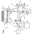
- FIG. 2 shows the laser connection device 10 with a radiation transmission device 56, which has a different structure with a changed arrangement of the infrared detector 47 compared to the radiation transmission device 12 in FIG. 1 .
- identical components are used in the laser connecting device 10 shown in FIG. 2 corresponding to the identically used reference numerals.
- the pivoting mirror means 29 and 30 are in a changed relative arrangement, such that the pivoting mirror means 29 has maintained its position and the pivoting mirror means 30 is now arranged below the pivoting mirror means 29.
- a radiation outcoupling device 57 is provided with a mirror surface 58 transparent to infrared radiation and highly reflecting for the laser radiation 27 of the laser emission device 11. This makes it possible, as shown in FIG. 2 , to arrange the infrared detector 47 without beam path deflection directly on the optical axis of the reflection of the terminal 20 infrared radiation. Overall, a more accurate detection of the infrared radiation component 45 is possible by the arrangement shown in FIG .
- FIG. 3 shows, according to the invention, a pressure device 50 with a transparent and rigid force introduction device 51, which can be formed, for example, from glass or a transparent epoxy resin.
- a transparent, incompressible and beyond deformable volume which is formed in the present case as a silicone pad 52.
- the silicon pad 52 is received in the present case by a receptacle 53 of the force introduction device 51, wherein the receptacle 53 is formed by a peripheral edge web 54 of the force introduction device 51.
- incompressible and deformable volume shows a liquid-analog printing behavior, so that, for example, deviations in the heights h and h 1 of the Kunststoffmetallmaschineen 23 of the substrate 17 by a corresponding deformation of the substrate 18 can be compensated.
- the edge web 54 serves as a deformation limit acting transversely to the printing direction.
- the use of the pressure pad 52 prevents the formation of gaps between the contact metallizations 23 and 24 of the oppositely arranged substrates 17 and 18 despite deviations in the heights h and h 1 of the contact metallizations 23.
Landscapes
- Engineering & Computer Science (AREA)
- Microelectronics & Electronic Packaging (AREA)
- Manufacturing & Machinery (AREA)
- Mechanical Engineering (AREA)
- Computer Hardware Design (AREA)
- Power Engineering (AREA)
- Physics & Mathematics (AREA)
- Optics & Photonics (AREA)
- Wire Bonding (AREA)
- Electric Connection Of Electric Components To Printed Circuits (AREA)
- Combinations Of Printed Boards (AREA)
- Laser Beam Processing (AREA)
Applications Claiming Priority (3)
| Application Number | Priority Date | Filing Date | Title |
|---|---|---|---|
| DE19751487 | 1997-11-20 | ||
| DE19751487A DE19751487A1 (de) | 1997-11-20 | 1997-11-20 | Verfahren und Vorrichtung zur thermischen Verbindung von Anschlußflächen zweier Substrate |
| EP98966159A EP1032482B1 (de) | 1997-11-20 | 1998-11-20 | Verfahren und vorrichtung zur thermischen verbindung von anschlussflächen zweier substrate |
Related Parent Applications (1)
| Application Number | Title | Priority Date | Filing Date |
|---|---|---|---|
| EP98966159.0 Division | 1998-11-20 |
Publications (2)
| Publication Number | Publication Date |
|---|---|
| EP1283085A1 EP1283085A1 (de) | 2003-02-12 |
| EP1283085B1 true EP1283085B1 (de) | 2005-06-01 |
Family
ID=7849341
Family Applications (2)
| Application Number | Title | Priority Date | Filing Date |
|---|---|---|---|
| EP02023748A Expired - Lifetime EP1283085B1 (de) | 1997-11-20 | 1998-11-20 | Verfahren und Vorrichtung zur thermischen Verbindung von Anschlussflächen zweier Substrate |
| EP98966159A Expired - Lifetime EP1032482B1 (de) | 1997-11-20 | 1998-11-20 | Verfahren und vorrichtung zur thermischen verbindung von anschlussflächen zweier substrate |
Family Applications After (1)
| Application Number | Title | Priority Date | Filing Date |
|---|---|---|---|
| EP98966159A Expired - Lifetime EP1032482B1 (de) | 1997-11-20 | 1998-11-20 | Verfahren und vorrichtung zur thermischen verbindung von anschlussflächen zweier substrate |
Country Status (6)
| Country | Link |
|---|---|
| US (1) | US6394158B1 (enExample) |
| EP (2) | EP1283085B1 (enExample) |
| JP (1) | JP2001523585A (enExample) |
| KR (1) | KR100565112B1 (enExample) |
| DE (3) | DE19751487A1 (enExample) |
| WO (1) | WO1999026753A1 (enExample) |
Families Citing this family (38)
| Publication number | Priority date | Publication date | Assignee | Title |
|---|---|---|---|---|
| DE19901623B4 (de) * | 1999-01-18 | 2007-08-23 | Pac Tech-Packaging Technologies Gmbh | Verfahren und Vorrichtung zur thermischen Verbindung von Anschlußflächen zweier Substrate |
| JP3914670B2 (ja) * | 1999-11-18 | 2007-05-16 | パイオニア株式会社 | 半導体モジュール及び半導体モジュールの半導体レーザ素子の取り付け方法 |
| DE10036900C2 (de) * | 2000-07-28 | 2002-07-11 | Siemens Ag | Verfahren zur Kontaktierung einer flexiblen Leiterplatte mit einem Kontaktpartner und Anordnung aus flexibler Leiterplatte und Kontaktpartner |
| EP1278240A2 (fr) | 2001-07-10 | 2003-01-22 | Koninklijke Philips Electronics N.V. | Procédé de report d'un composant sur un support de connexion par soudage sans apport de matière |
| DE10133731C2 (de) * | 2001-07-11 | 2003-08-14 | Huf Tools Gmbh | Verfahren zum Herstellen eines elektrischen Endprodukts, welches Löt-oder Schweißstellen aufweist |
| US6706402B2 (en) | 2001-07-25 | 2004-03-16 | Nantero, Inc. | Nanotube films and articles |
| US6574130B2 (en) | 2001-07-25 | 2003-06-03 | Nantero, Inc. | Hybrid circuit having nanotube electromechanical memory |
| US6924538B2 (en) | 2001-07-25 | 2005-08-02 | Nantero, Inc. | Devices having vertically-disposed nanofabric articles and methods of making the same |
| US7259410B2 (en) | 2001-07-25 | 2007-08-21 | Nantero, Inc. | Devices having horizontally-disposed nanofabric articles and methods of making the same |
| US7335395B2 (en) | 2002-04-23 | 2008-02-26 | Nantero, Inc. | Methods of using pre-formed nanotubes to make carbon nanotube films, layers, fabrics, ribbons, elements and articles |
| EP1424156A1 (en) * | 2002-11-29 | 2004-06-02 | Leica Geosystems AG | Process for soldering miniaturized components onto a base plate |
| US6796636B2 (en) * | 2002-12-17 | 2004-09-28 | Lexmark International, Inc. | Two shot molded inkjet printhead lid for laser welding |
| DE10361521A1 (de) * | 2003-12-03 | 2005-07-07 | Pac Tech - Packaging Technologies Gmbh | Verfahren und Vorrichtung zur wechselseitigen Kontaktierung von zwei Wafern |
| JP5230099B2 (ja) * | 2003-12-03 | 2013-07-10 | パック テック−パッケージング テクノロジーズ ゲーエムベーハー | 2つのウェーハを相互接触させる方法および装置 |
| US7205938B2 (en) * | 2004-03-05 | 2007-04-17 | Airespace, Inc. | Wireless node location mechanism responsive to observed propagation characteristics of wireless network infrastructure signals |
| US7187066B2 (en) * | 2004-09-22 | 2007-03-06 | Intel Corporation | Radiant energy heating for die attach |
| KR100740762B1 (ko) * | 2005-02-10 | 2007-07-19 | 오므론 가부시키가이샤 | 접합 방법 및 접합 장치 |
| US20060196600A1 (en) * | 2005-03-03 | 2006-09-07 | Gi-Jung Nam | Apparatus and method for bonding anisotropic conductive film using laser beam |
| US7538295B2 (en) * | 2005-04-21 | 2009-05-26 | Hewlett-Packard Development Company, L.P. | Laser welding system |
| KR101113850B1 (ko) * | 2005-08-11 | 2012-02-29 | 삼성테크윈 주식회사 | 플립 칩 본딩 방법 및 이를 채택한 플립 칩 본딩 장치 |
| FR2895924B1 (fr) | 2006-01-10 | 2009-09-25 | Valeo Electronique Sys Liaison | Procede de brasage entre eux d'au moins deux organes empiles |
| JP4514722B2 (ja) * | 2006-02-20 | 2010-07-28 | 富士通セミコンダクター株式会社 | フィルム貼り付け方法、フィルム貼り付け装置および半導体装置の製造方法 |
| JP4880561B2 (ja) * | 2007-10-03 | 2012-02-22 | 新光電気工業株式会社 | フリップチップ実装装置 |
| US20090120916A1 (en) * | 2007-11-12 | 2009-05-14 | L3 Communications Corporation | Through-Via Laser Reflow Systems And Methods For Surface Mount Components |
| NL2001958C (en) * | 2008-09-05 | 2010-03-15 | Stichting Energie | Method of monolithic photo-voltaic module assembly. |
| JP5294916B2 (ja) * | 2009-02-17 | 2013-09-18 | パナソニック株式会社 | レーザはんだ付け装置 |
| DE102009017659A1 (de) * | 2009-04-16 | 2010-10-28 | Schott Ag | Verfahren zur leitenden Verbindung eines Bauelementes auf einem transprenten Substrat |
| DE102010015520A1 (de) * | 2010-04-16 | 2011-10-20 | Pac Tech-Packaging Technologies Gmbh | Verfahren und Vorrichtung zur Ausbildung von Lotdepots |
| JP5589584B2 (ja) * | 2010-06-16 | 2014-09-17 | 凸版印刷株式会社 | レーザ溶接方法、電子部品接続構造及びレーザ溶接検査方法 |
| KR20140014156A (ko) * | 2011-02-02 | 2014-02-05 | 파크 테크-파카징 테크놀로지이스 게엠베하 | 기체상의 플럭스 매체를 이용한 레이저 납땜에 의한 두 기판의 접속 영역의 전기적인 본딩 방법 및 장치 |
| DE102011104159A1 (de) * | 2011-06-14 | 2012-12-20 | Institut Für Solarenergieforschung Gmbh | Verfahren zum elektrischen verbinden mehrerer solarzellen und photovoltaikmodul |
| KR20130039955A (ko) * | 2011-10-13 | 2013-04-23 | 현대자동차주식회사 | 용접용 레이저 장치 |
| US10099315B2 (en) * | 2014-06-27 | 2018-10-16 | Jabil Inc. | System, apparatus and method for hybrid function micro welding |
| DE102015216205A1 (de) * | 2015-08-25 | 2017-03-02 | Continental Teves Ag & Co. Ohg | Verfahren zum Herstellen einer Steckverbindung, Verfahren zum Verstärken einer Steckverbindung und Vorrichtung |
| FR3061801A1 (fr) * | 2017-01-12 | 2018-07-13 | Commissariat Energie Atomique | Procede de connexion electrique entre au moins deux elements |
| KR20180137888A (ko) | 2017-06-20 | 2018-12-28 | 주식회사 프로텍 | 반도체 칩 본딩 장치 및 반도체 칩 본딩 방법 |
| KR101975103B1 (ko) | 2017-06-20 | 2019-05-03 | 주식회사 프로텍 | 플립칩 레이저 본딩 장치 및 플립칩 레이저 본딩 방법 |
| KR102394825B1 (ko) | 2020-04-23 | 2022-05-06 | 주식회사 프로텍 | 빅셀 소자를 이용한 플립칩 본딩 장치 |
Family Cites Families (29)
| Publication number | Priority date | Publication date | Assignee | Title |
|---|---|---|---|---|
| DE140942C (enExample) | ||||
| US3503804A (en) * | 1967-04-25 | 1970-03-31 | Hellmut Schneider | Method and apparatus for the production of sonic or ultrasonic waves on a surface |
| JPS5132836Y2 (enExample) * | 1972-02-04 | 1976-08-16 | ||
| DE2335517C3 (de) | 1973-07-12 | 1980-04-30 | Siemens Ag, 1000 Berlin Und 8000 Muenchen | Verfahren zur Kompensation von Lageabweichungen eines Zifferblattes oder Schildes relativ zu einem Beschriftungsgerät |
| DD140942A1 (de) * | 1978-12-20 | 1980-04-02 | Horst Ahlers | Verfahren und anordnung zur mikroverbindungstechnik mittels laser |
| DE3247338A1 (de) * | 1982-12-21 | 1984-06-28 | Siemens AG, 1000 Berlin und 8000 München | Verfahren zum laserloeten von flexiblen verdrahtungen |
| JPS60172023A (ja) * | 1984-02-17 | 1985-09-05 | Nec Corp | レ−ザ集光装置 |
| JPS6261789A (ja) * | 1985-09-09 | 1987-03-18 | Fuji Electric Co Ltd | レ−ザ溶接方法 |
| JPS62108224A (ja) * | 1985-11-06 | 1987-05-19 | Inoue Japax Res Inc | レ−ザ用レンズ |
| US4863538A (en) * | 1986-10-17 | 1989-09-05 | Board Of Regents, The University Of Texas System | Method and apparatus for producing parts by selective sintering |
| JPS6421997A (en) * | 1987-07-16 | 1989-01-25 | Toshiba Corp | Method of soldering electronic component |
| US4845335A (en) * | 1988-01-28 | 1989-07-04 | Microelectronics And Computer Technology Corporation | Laser Bonding apparatus and method |
| US4978835A (en) * | 1989-08-21 | 1990-12-18 | Microelectronics And Computer Technology Corporation | Method of clamping electrical contacts for laser bonding |
| FR2653367A1 (fr) | 1989-10-24 | 1991-04-26 | Quantel Sa | Procede et appareil de brasage au laser. |
| FR2659886A1 (fr) | 1990-03-26 | 1991-09-27 | Mafond Luc | Procede et dispositif destines au chauffage d'une matiere de soudage. |
| GB2244374B (en) * | 1990-05-22 | 1994-10-05 | Stc Plc | Improvements in hybrid circuits |
| JPH0491493A (ja) | 1990-08-01 | 1992-03-24 | Nippon Mektron Ltd | レーザー半田付け方法とその装置 |
| US5055652A (en) * | 1990-10-01 | 1991-10-08 | General Electric Company | Laser soldering of flexible leads |
| JPH04237589A (ja) * | 1991-01-21 | 1992-08-26 | Nec Corp | レーザ加工装置 |
| DE4111247C3 (de) * | 1991-04-08 | 1996-11-21 | Export Contor Ausenhandelsgese | Schaltungsanordnung |
| JPH05109824A (ja) * | 1991-10-15 | 1993-04-30 | Omron Corp | 電子部品のフリツプチツプ実装方法 |
| JPH0758448A (ja) * | 1993-08-09 | 1995-03-03 | Mitsubishi Electric Corp | レーザーボンディング装置及び方法 |
| DE4446289C2 (de) * | 1994-12-23 | 1999-02-11 | Finn David | Verfahren zur Mikroverbindung von Kontaktelementen |
| DE19549635B4 (de) * | 1995-02-15 | 2004-12-09 | Fraunhofer-Gesellschaft zur Förderung der angewandten Forschung e.V. | Verfahren zur Verbindung eines flexiblen Substrats mit einem Chip |
| JP3285294B2 (ja) * | 1995-08-08 | 2002-05-27 | 太陽誘電株式会社 | 回路モジュールの製造方法 |
| JP3779358B2 (ja) * | 1995-10-06 | 2006-05-24 | ソニー株式会社 | 立体形状造形方法 |
| JPH09199846A (ja) * | 1996-01-19 | 1997-07-31 | Toshiba Electron Eng Corp | 電子部品実装方法および電子部品実装装置 |
| JP3746555B2 (ja) * | 1996-02-06 | 2006-02-15 | 株式会社フジクラ | レーザ加工装置およびこれを用いたレーザ加工方法 |
| US5847356A (en) * | 1996-08-30 | 1998-12-08 | Hewlett-Packard Company | Laser welded inkjet printhead assembly utilizing a combination laser and fiber optic push connect system |
-
1997
- 1997-11-20 DE DE19751487A patent/DE19751487A1/de not_active Ceased
-
1998
- 1998-11-20 WO PCT/DE1998/003439 patent/WO1999026753A1/de not_active Ceased
- 1998-11-20 EP EP02023748A patent/EP1283085B1/de not_active Expired - Lifetime
- 1998-11-20 DE DE59809879T patent/DE59809879D1/de not_active Expired - Lifetime
- 1998-11-20 US US09/554,898 patent/US6394158B1/en not_active Expired - Lifetime
- 1998-11-20 EP EP98966159A patent/EP1032482B1/de not_active Expired - Lifetime
- 1998-11-20 KR KR1020007005515A patent/KR100565112B1/ko not_active Expired - Lifetime
- 1998-11-20 JP JP2000521942A patent/JP2001523585A/ja active Pending
- 1998-11-20 DE DE59812840T patent/DE59812840D1/de not_active Expired - Lifetime
Also Published As
| Publication number | Publication date |
|---|---|
| US6394158B1 (en) | 2002-05-28 |
| DE59812840D1 (de) | 2005-07-07 |
| EP1283085A1 (de) | 2003-02-12 |
| KR20010032305A (ko) | 2001-04-16 |
| EP1032482A1 (de) | 2000-09-06 |
| DE59809879D1 (de) | 2003-11-13 |
| KR100565112B1 (ko) | 2006-03-30 |
| JP2001523585A (ja) | 2001-11-27 |
| WO1999026753A1 (de) | 1999-06-03 |
| EP1032482B1 (de) | 2003-10-08 |
| DE19751487A1 (de) | 1999-06-02 |
Similar Documents
| Publication | Publication Date | Title |
|---|---|---|
| EP1283085B1 (de) | Verfahren und Vorrichtung zur thermischen Verbindung von Anschlussflächen zweier Substrate | |
| DE68926448T2 (de) | Bildsensor und verfahren zu dessen herstellung | |
| DE69408558T2 (de) | Verwendung einer anisotropischen leitfähigen Schicht für die Verbindung von Anschlussleitern einer Leiterplatte mit den elektrischen Anschlusskontakten einer photoelektrischen Umwandlungsvorrichtung und Verfahren zur Montage dieser Vorrichtung | |
| EP2016449B1 (de) | Verfahren zur herstellung eines optoelektronischen bauelements | |
| DE68911420T2 (de) | Festkörper-Bildaufnahmevorrichtung. | |
| DE19549635B4 (de) | Verfahren zur Verbindung eines flexiblen Substrats mit einem Chip | |
| DE19932430C2 (de) | Opto-elektronische Baugruppe sowie Bauteil für diese Baugruppe | |
| DE69008480T2 (de) | Gehäuse für einen Festkörperbildsensor. | |
| DE69702562T2 (de) | Halbleiterlasermodul | |
| DE3834335A1 (de) | Halbleiterschaltung | |
| DE19621124A1 (de) | Optoelektronischer Wandler und dessen Herstellungsverfahren | |
| DE3829553A1 (de) | Optischer aufzeichnungskopf | |
| DE19502264C2 (de) | Modul für eine optische Verbindung | |
| DE69935129T2 (de) | Ein verfahren zur herstellung von spiegeln in polymerwellenleitern | |
| DE68929527T2 (de) | Optische Übertragungsvorrichtung | |
| DE69534526T2 (de) | Selbstjustierendes optisches Element und optischer Wellenleiter durch Löthöcker auf rechteckiger Platte | |
| DE69009625T2 (de) | Zusammenbau von Teilen mit einem gegenseitigen Winkel und Verfahren zur Herstellung. | |
| DE69015588T2 (de) | Optischer Kopf integrierbar in einem hybriden Schaltkreis. | |
| DE69325696T2 (de) | Bildsensorvorrichtung für direkten Kontakt und Bildsensoreinheit | |
| DE102007007355B4 (de) | Verfahren zur Herstellung optischer Verbindungen und optische Anordnung | |
| DE3851482T2 (de) | Bildsensor vom Typ Kontakt. | |
| WO2008022609A1 (de) | Optisches koppelelement | |
| WO2024002691A1 (de) | Vorrichtung und verfahren zur herstellung einer kontaktverbindung | |
| DE19704502C1 (de) | Lasermodul mit Ankoppeloptik und Verfahren zur Feinjustierung der Ankoppeloptik | |
| DE19749909C2 (de) | Vorrichtung zum Herstellen von Verbindungen zwischen jeweils zwei Kontaktelementen mittels Laserenergie |
Legal Events
| Date | Code | Title | Description |
|---|---|---|---|
| PUAI | Public reference made under article 153(3) epc to a published international application that has entered the european phase |
Free format text: ORIGINAL CODE: 0009012 |
|
| AC | Divisional application: reference to earlier application |
Ref document number: 1032482 Country of ref document: EP Kind code of ref document: P |
|
| AK | Designated contracting states |
Designated state(s): DE GB |
|
| 17P | Request for examination filed |
Effective date: 20021024 |
|
| AKX | Designation fees paid |
Designated state(s): DE GB |
|
| R17P | Request for examination filed (corrected) |
Effective date: 20030812 |
|
| GRAP | Despatch of communication of intention to grant a patent |
Free format text: ORIGINAL CODE: EPIDOSNIGR1 |
|
| GRAS | Grant fee paid |
Free format text: ORIGINAL CODE: EPIDOSNIGR3 |
|
| GRAA | (expected) grant |
Free format text: ORIGINAL CODE: 0009210 |
|
| AC | Divisional application: reference to earlier application |
Ref document number: 1032482 Country of ref document: EP Kind code of ref document: P |
|
| AK | Designated contracting states |
Kind code of ref document: B1 Designated state(s): DE GB |
|
| REG | Reference to a national code |
Ref country code: GB Ref legal event code: FG4D Free format text: NOT ENGLISH |
|
| REF | Corresponds to: |
Ref document number: 59812840 Country of ref document: DE Date of ref document: 20050707 Kind code of ref document: P |
|
| GBT | Gb: translation of ep patent filed (gb section 77(6)(a)/1977) |
Effective date: 20050622 |
|
| PLBE | No opposition filed within time limit |
Free format text: ORIGINAL CODE: 0009261 |
|
| STAA | Information on the status of an ep patent application or granted ep patent |
Free format text: STATUS: NO OPPOSITION FILED WITHIN TIME LIMIT |
|
| 26N | No opposition filed |
Effective date: 20060302 |
|
| PGFP | Annual fee paid to national office [announced via postgrant information from national office to epo] |
Ref country code: GB Payment date: 20151123 Year of fee payment: 18 |
|
| PGFP | Annual fee paid to national office [announced via postgrant information from national office to epo] |
Ref country code: DE Payment date: 20160121 Year of fee payment: 18 |
|
| REG | Reference to a national code |
Ref country code: DE Ref legal event code: R119 Ref document number: 59812840 Country of ref document: DE |
|
| GBPC | Gb: european patent ceased through non-payment of renewal fee |
Effective date: 20161120 |
|
| PG25 | Lapsed in a contracting state [announced via postgrant information from national office to epo] |
Ref country code: GB Free format text: LAPSE BECAUSE OF NON-PAYMENT OF DUE FEES Effective date: 20161120 Ref country code: DE Free format text: LAPSE BECAUSE OF NON-PAYMENT OF DUE FEES Effective date: 20170601 |