EP1237282B1 - Schaltung zur Detektion von Störungen der Periodendauer in einem Taktsignal - Google Patents
Schaltung zur Detektion von Störungen der Periodendauer in einem Taktsignal Download PDFInfo
- Publication number
- EP1237282B1 EP1237282B1 EP02250671A EP02250671A EP1237282B1 EP 1237282 B1 EP1237282 B1 EP 1237282B1 EP 02250671 A EP02250671 A EP 02250671A EP 02250671 A EP02250671 A EP 02250671A EP 1237282 B1 EP1237282 B1 EP 1237282B1
- Authority
- EP
- European Patent Office
- Prior art keywords
- circuit
- signal
- flip
- clock
- flop circuit
- Prior art date
- Legal status (The legal status is an assumption and is not a legal conclusion. Google has not performed a legal analysis and makes no representation as to the accuracy of the status listed.)
- Expired - Lifetime
Links
Images

Classifications
-
- G—PHYSICS
- G06—COMPUTING OR CALCULATING; COUNTING
- G06F—ELECTRIC DIGITAL DATA PROCESSING
- G06F1/00—Details not covered by groups G06F3/00 - G06F13/00 and G06F21/00
- G06F1/04—Generating or distributing clock signals or signals derived directly therefrom
- G06F1/14—Time supervision arrangements, e.g. real time clock
-
- G—PHYSICS
- G01—MEASURING; TESTING
- G01R—MEASURING ELECTRIC VARIABLES; MEASURING MAGNETIC VARIABLES
- G01R31/00—Arrangements for testing electric properties; Arrangements for locating electric faults; Arrangements for electrical testing characterised by what is being tested not provided for elsewhere
- G01R31/28—Testing of electronic circuits, e.g. by signal tracer
- G01R31/317—Testing of digital circuits
- G01R31/31727—Clock circuits aspects, e.g. test clock circuit details, timing aspects for signal generation, circuits for testing clocks
-
- H—ELECTRICITY
- H03—ELECTRONIC CIRCUITRY
- H03K—PULSE TECHNIQUE
- H03K5/00—Manipulating of pulses not covered by one of the other main groups of this subclass
- H03K5/159—Applications of delay lines not covered by the preceding subgroups
-
- H—ELECTRICITY
- H03—ELECTRONIC CIRCUITRY
- H03K—PULSE TECHNIQUE
- H03K5/00—Manipulating of pulses not covered by one of the other main groups of this subclass
- H03K5/19—Monitoring patterns of pulse trains
Definitions
- the present invention relates to a monitoring circuit for determining whether the period of a clock signal has become shorter than a predetermined permissible range.
- MPUs Micro Processing Units
- processors such as MPUs are designed to operate in synchronization with a clock signal of a predetermined period and are therefore subject to overrunning when the period of this clock signal has become shorter than the predetermined period.
- SU-A-1 798 919 discloses a device for monitoring clock signals.
- the device comprises a first D-flip-flop, a delay line and a second D-flip-flop configured in a ring; a delay line, a reset line and an output line.
- the device is reset by feeding a '1' to the reset line whereby the first D-flip-flop is set and the second D-flip-flop is reset.
- a sync signal is fed to the clock input of the first D-flip-flop.
- the pulse train which is to be monitored is fed to the clock input of the second D-flip-flop.
- a status signal is derived from the output of the first D-flip-flop.
- the invention seeks to provide for a clock monitoring circuit having advantage over known such circuits.
- a clock monitoring circuit comprising a first flip-flop circuit for latching and outputting an input signal when a given transition of a clock signal occurs between its two logic levels, a second flip-flop circuit for latching and outputting the output signal of the first flip-flop circuit when a given transition of the clock signal occurs between its two logic levels, delay means for delaying the output signal of the second flip-flop circuit by a time interval that is shorter than a predetermined period of the clock signal and for outputting the resultant signal as an input signal to the first flip-flop circuit, and a gate circuit for receiving the output signal of the first flip-flop circuit and the output signal of the second flip-flop circuit, and for outputting a signal of a first logic level when the period of the clock signal is equal to, or greater than, the predetermined time interval and for outputting a signal of a second logic level when the period of the clock signal is shorter than the predetermined time interval, and further comprising a third flip-flop circuit for latching the output signal of the gate circuit at a
- the gate circuit is arranged such that it receives the output signals of the first and second flip-flop circuits and provides an output signal whose logic level depends on whether the period of the input clock signals is the predetermined period or not. A shortening of the period of the clock signal can thus be detected according to the logic level of the output signal of the clock monitoring circuit.
- the aforementioned clock monitoring circuit When an abnormality in the clock signal is detected by the clock monitoring circuit, this abnormality is communicated to a control circuit that controls the operation of the processor, thereby halting the operation of the processor.
- the present invention can thus provide a clock monitoring circuit that can easily and accurately detect that the period of a clock signal has become shorter than a predetermined period.
- the invention can therefore be used in a data processing device that is equipped with the above-described clock monitoring circuit and that can prevent overrunning of a processing circuit when the period of the clock signal has become shorter than the predetermined period.
- a data processing device which uses an embodiment of the present invention and which includes a reset input terminal 102, a plurality of data input/output terminals 103, a clock generating circuit 104, a Micro Processing Unit (MPU) 105 for data processing, a clock monitoring circuit 106, and an operation control circuit 107.
- MPU Micro Processing Unit
- the reset input terminal 102 is connected to the MPU 105 and the clock monitoring circuit 106 and the data input/output terminal 103 is connected to the MPU 105.
- the MPU 105 is further connected to the clock generating circuit 104 and also the operation control circuit 107.
- the clock monitoring circuit 106 is also connected to the clock generating circuit 104 and to the operation control circuit 107.
- the clock generating circuit 104 is provided with, for example, a crystal oscillator (not shown), and is arranged to generate a clock signal of a predetermined period T.
- a computer program for controlling processing i.e. software or firmware, is installed in the MPU 105, and the MPU 105 executes appropriate processing steps in synchronization with the clock signal generated by the clock generating circuit 104.
- the MPU 105 executes processing steps in accordance with the various types of data that are supplied from data input/output terminals 103, and outputs the resulting data from data input/output terminals 103. Accordingly, the data processor can communicate with external apparatus (not shown) by way of the data input/output terminals 103, and can execute various types of data processing steps in accordance with this communication.
- the reset signal When a reset signal is applied as input to the reset input terminal 102, the reset signal is applied to the MPU 105 and the clock monitoring circuit 106, whereby the MPU 105 and the clock monitoring circuit 106 are reset.
- the clock monitoring circuit 106 monitors the period of the clock signal generated by the clock generating circuit 104. When the period of the clock signal becomes shorter than a predetermined reference time interval, the clock monitoring circuit 106 provides a clock abnormality signal for the operation control circuit 107. When the operation control circuit 107 receives the clock abnormality signal from clock monitoring circuit 106, it forcibly halts the processing performed by the MPU 105.
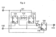
- the clock monitoring circuit of this embodiment comprises a reset input terminal 111, a clock input terminal 112, a signal output terminal 113, a flip-flop (hereinafter abbreviated to FF) circuit 114, a signal delay circuit 115, a FF circuit 116, an exclusive-OR circuit 117, an inverter element 118, an inverter element 119, and a FF circuit 120.
- FF flip-flop
- the reset input terminal 111 is connected to the reset terminal of the FF circuit 114, the set terminal of the FF circuit 116, and the reset terminal of the FF circuit 120.
- the clock input terminal 112 is connected to the clock terminals of the FF circuit 114 and the FF circuit 116, and to the clock terminal of the FF circuit 120 by way of the inverter element 119.
- the signal input terminal of the FF circuit 114 and the signal output terminal of the FF circuit 116 are connected to each other through a feedback signal 121.
- the signal output terminal of the FF circuit 114 and the signal input terminal of the FF circuit 116 are connected by way of the signal delay circuit 115.
- the signal output terminals of the FF circuit 114 and the FF circuit 116 are each connected to a respective signal input terminal of the exclusive-OR circuit 117.
- the signal output terminal of the exclusive-OR circuit 117 is connected to the signal input terminal of the FF circuit 120 by way of the inverter element 118.
- the signal output terminal of the FF circuit 120 is connected to the signal output terminal 113, and signal output terminal 113 is connected to the operation control circuit 107 (Fig. 1).
- the FF circuit 114 is reset by the reset signal.
- the FF circuit 114 is arranged to receive an output signal Q 2 of the FF circuit 116 as input signal D 1 . It then latches the input signal D 1 at the rising edge of an input clock signal CLK, and provides an output signal Q 1 as an input to the signal delay circuit 115.
- the signal delay circuit 115 is made up of two inverter elements that are connected in series.
- the signal delay circuit 115 delays the output signal Q 1 from the FF circuit 114 by a predetermined time interval, and provides an input signal D 2 to the FF circuit 116. This delay time must be set shorter than the period of the normal clock signal and longer than the minimum period of the clock signal at which the MPU 105 can operate normally.
- the FF circuit 116 is arranged to be set by the reset signal, to receive the input signal D 2 , to latch the input signal D 2 at the rising edge of the received clock signal CLK, and to provide an output signal Q 2 as an output.
- the output signal Q 2 is supplied as an input signal D 1 to the FF circuit 114.
- the exclusive-OR circuit 117 exclusively ORs the output signal Q 1 from the FF circuit 114 with an output signal Q 2 from the FF circuit 116 and provides the resultant signal as an output.
- the inverter element 118 serves to invert the output signal of the exclusive-OR circuit 117 and provides the resultant signal as an input signal D 3 to the FF circuit 120.
- the FF circuit 120 is arranged to be reset by the reset signal, to receive the input signal D 3 that is output from inverter 118, to latch the input signal D 3 at the rising edge of clock signal CLK that was inverted by inverter element 119, and to provide output signal Q 3 as an output.
- Output signal Q 3 of the FF circuit 120 is supplied to the operation control circuit 107 by way of the signal output terminal 113.
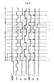
- the output signal Q 1 of the FF circuit 114 is delayed a predetermined time interval by the signal delay circuit 115.
- the FF circuit 116 receives the delayed signal, i.e., the input signal D 2 at the rising edge of the clock signal CLK, and provides the signal as the output signal Q 2 .
- the output signal Q 1 of the FF circuit 114 becomes a signal that is the inverted logic of the output signal Q 2 of the FF circuit 116. Also, the output signal Q 2 of the FF circuit 116 becomes a signal that is the inverted logic of the output signal Q 1 of the FF circuit 114. Accordingly, the output signal of the exclusive OR circuit 117 Is maintained at a low logical level.
- the FF circuit 120 receives, as its input signal D 3 , the output signal of the exclusive-OR circuit 117 that has been inverted by the inverter element 118, and by matching the logic level of the output signal Q 3 with the logic level of the input signal D 3 at the rising edge of the clock signal CLK that is inverted by the inverter element 119.
- the spike noise that occurs in the output signal D 3 of the exclusive-OR circuit 117 due to the timing error between the FF circuit 114 and the FF circuit 116 is eliminated.
- the output signal Q 1 of the FF circuit 114 and the output signal Q 2 of the FF circuit 116 both go low between time t 2 and time t 3 .
- the input signal D 3 of the FF circuit 120 accordingly goes high.
- the output signal Q 3 also goes high, and a clock abnormality signal is transmitted as output from the output terminal 113 to the operation control circuit 107.
- the operation control circuit 107 receives the clock abnormality signal and forcibly halts the operation of the MPU 105, thereby reliably preventing overrunning of the MPU 105.
- the clock monitoring circuit 106 When the period of the clock signal CLK returns to T at time t 4 , the clock monitoring circuit 106 operates as previously described.
- the clock monitoring circuit 106 of the present embodiment since the signal delay circuit 115 is constituted by logic circuits, the delay time of the signal delay circuit 115 does not vary in analog fashion, and since the clock monitoring circuit itself comprises by digital circuits, the clock monitoring circuit 106 is capable of stable operation.
- the present invention is not limited to the above-described embodiment, and allows various modifications within the scope of the invention.
- the signal delay circuit 115 is formed by logic circuits and the clock monitoring circuit 106 is formed entirely by digital circuits in the above-described embodiment, an analog signal delay circuit comprising, for example, resistors and capacitors, or a signal delay circuit comprising a long wiring may also be used.
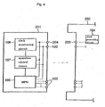
- the data processing system 200 may be formed in a manner which includes a data processor 201 that does not incorporate a clock generating circuit, as shown in Fig. 4.
- the data processing system 200 comprises parent device 202 which can be equipped with the data processor 201 as a subordinate device, and the parent device 202 comprises clock generating circuit 104 and clock output terminal 203.
- the data processor 201 can include a clock input terminal 204, and the clock input terminal 204 and the clock output terminal 203 are then connected when the data processor 201 includes the parent device 202.
- the clock signal generated by the clock generating circuit 104 of the parent device 202 is supplied from the clock output terminal 203 to the clock input terminal 204 of the data processor 201, and each of the portions 105-107 of the data processing device 201 operate in synchronization with the clock signal.
- a clock signal is supplied from the parent device 202 to the data processor 201 in the data processing system 200.
- the data processor 201 can accept parent devices of a variety of standards, and a clock signal having a period that is shorter than the predetermined period may be supplied to the data processor 201.
- the data processing device 201 comprises the clock monitoring circuit 106 and the operation control circuit 107, and thereby prevents overrunning of the MPU 105.
- the FF circuit 114 and the FF circuit 116 are designed to operate at the rising edge of the clock signal CLK, and the FF circuit 120 is designed to operate at the falling edge of the clock signal CLK in the clock monitoring circuit 106 of this embodiment, the FF circuit 114 and the FF circuit 116 may be designed to operate at the falling edge of clock signal CLK and the FF circuit 120 may be designed to operate at the rising edge of the clock signal CLK.
- inverted output signals Q may be used as the output signals of the FF circuit 114, the FF circuit 116, and the FF circuit 120, respectively, instead of the output signals Q 1 , Q 2 , and Q 3 .
Landscapes
- Physics & Mathematics (AREA)
- Engineering & Computer Science (AREA)
- Nonlinear Science (AREA)
- General Engineering & Computer Science (AREA)
- General Physics & Mathematics (AREA)
- Theoretical Computer Science (AREA)
- Manipulation Of Pulses (AREA)
- Pulse Circuits (AREA)
Claims (5)
- Taktüberwachungsschaltung (106) mit einer ersten Flipflopschaltung (116) zum Zwischenspeichern und Ausgeben eines Eingangssignals, wenn ein vorgegebener Übergang eines Taktsignals zwischen seinen beiden Logikpegeln auftritt, einer zweiten Flipflopschaltung (114) zum Zwischenspeichern und Ausgeben des Ausgangssignals der ersten Flipflopschaltung (116), wenn ein vorgegebener Übergang des Taktsignals zwischen seinen beiden Logikpegeln auftritt, einer Verzögerungseinrichtung (115) zum Verzögern des Ausgangssignals der zweiten Flipflopschaltung (114) um ein Zeitintervall, das kürzer als eine vorbestimmte Periode des Taktsignals ist, und zum Ausgeben des resultierenden Signals als Eingangssignal zur ersten Flipflopschaltung (116), und einer Gatterschaltung (117) zum Empfangen des Ausgangssignals der ersten Flipflopschaltung (116) und des Ausgangssignals der zweiten Flipflopschaltung (114) und zum Ausgeben eines Signals mit einem ersten Logikpegel, wenn die Periode des Taktsignals gleich oder größer als das vorbestimmte Zeitintervall ist, und zum Ausgeben eines Signals mit einem zweiten Logikpegel, wenn die Periode des Taktsignals kürzer als das vorbestimmte Zeitintervall ist, und ferner mit einer dritten Flipflopschaltung (120) zum Zwischenspeichern des Ausgangssignals der Gatterschaltung (117) bei einer Taktung, die gegenüber der Zwischenspeicherung der zweiten Flipflopschaltung (114) verzögert ist, wenn ein vorgegebener Übergang des Taktsignals zwischen seinen beiden Logikpegeln auftritt.
- Schaltung nach Anspruch 1, wobei der positive Ausgangsanschluß der ersten Flipflopschaltung (116) mit dem Eingangsanschluß der zweiten Flipflopschaltung (114) verbunden ist und der Eingangsanschluß der Verzögerungseinrichtung (115) mit dem positiven Ausgangsanschluß der zweiten Flipflopschaltung (114) verbunden ist und wobei die Gatterschaltung (117) eine Exklusiv-ODER-Schaltung aufweist, die eine Exklusiv-ODER-Verknüpfung des Ausgangssignals des positiven Ausgangsanschlusses der ersten Flipflopschaltung (116) mit dem Ausgangssignal des positiven Ausgangsanschlusses der zweiten Flipflopschaltung (114) vornimmt.
- Schaltung nach Anspruch 1 oder 2, wobei die Verzögerungseinrichtung (115) eine Logikschaltungseinrichtung aufweist.
- Schaltung nach Anspruch 3, wobei die Verzögerungseinrichtung (115) mehrere in Reihe geschaltete Inverterelemente aufweist.
- Schaltung nach Anspruch 2, ferner mit einer dritten Flipflopschaltung zum Zwischenspeichern und Ausgeben des Ausgangssignals der Exklusiv-ODER-Schaltung oder des invertierten Signals des Ausgangssignals der Exklusiv-ODER-Schaltung bei einer Taktung, die gegenüber der Zwischenspeicherung der zweiten Flipflopschaltung verzögert ist, wenn ein vorgegebener Übergang des Taktsignals zwischen seinen beiden Logikpegeln auftritt.
Applications Claiming Priority (2)
| Application Number | Priority Date | Filing Date | Title |
|---|---|---|---|
| JP2001048354 | 2001-02-23 | ||
| JP2001048354A JP2002251227A (ja) | 2001-02-23 | 2001-02-23 | クロック監視回路、データ処理装置、データ処理システム |
Publications (2)
| Publication Number | Publication Date |
|---|---|
| EP1237282A1 EP1237282A1 (de) | 2002-09-04 |
| EP1237282B1 true EP1237282B1 (de) | 2003-10-08 |
Family
ID=18909635
Family Applications (1)
| Application Number | Title | Priority Date | Filing Date |
|---|---|---|---|
| EP02250671A Expired - Lifetime EP1237282B1 (de) | 2001-02-23 | 2002-01-31 | Schaltung zur Detektion von Störungen der Periodendauer in einem Taktsignal |
Country Status (7)
| Country | Link |
|---|---|
| US (1) | US6545508B2 (de) |
| EP (1) | EP1237282B1 (de) |
| JP (1) | JP2002251227A (de) |
| KR (1) | KR20020069143A (de) |
| DE (1) | DE60200050T2 (de) |
| HK (1) | HK1047356A1 (de) |
| SG (1) | SG96682A1 (de) |
Families Citing this family (18)
| Publication number | Priority date | Publication date | Assignee | Title |
|---|---|---|---|---|
| JP3476448B2 (ja) * | 2001-12-12 | 2003-12-10 | 沖電気工業株式会社 | 信号同期回路 |
| JP3848152B2 (ja) * | 2001-12-20 | 2006-11-22 | 株式会社東芝 | 多機能icカード |
| FR2875311A1 (fr) * | 2004-09-14 | 2006-03-17 | St Microelectronics Sa | Procede de detection du positionnement relatif de deux signaux et dispositif correspondant |
| US20060193417A1 (en) * | 2005-02-25 | 2006-08-31 | Tellabs Operations, Inc. | Systems and methods for switching between redundant clock signals |
| US7622961B2 (en) * | 2005-09-23 | 2009-11-24 | Intel Corporation | Method and apparatus for late timing transition detection |
| JP2007121114A (ja) * | 2005-10-28 | 2007-05-17 | Elpida Memory Inc | デューティ検知回路、これらを備えたdll回路及び半導体装置 |
| DE102005060394B4 (de) * | 2005-12-16 | 2012-10-11 | Infineon Technologies Ag | Schaltungsanordnung und Verfahren zum Betreiben einer Schaltungsanordnung |
| US7480838B1 (en) * | 2006-03-23 | 2009-01-20 | Intel Corporation | Method, system and apparatus for detecting and recovering from timing errors |
| US7679404B2 (en) * | 2006-06-23 | 2010-03-16 | Intel Corporation | Missing clock pulse detector |
| US7498848B2 (en) * | 2006-10-03 | 2009-03-03 | Freescale Semiconductor, Inc. | System and method for monitoring clock signal in an integrated circuit |
| DE602008003051D1 (de) * | 2007-05-18 | 2010-12-02 | St Microelectronics Rousset | Erkennung einer Zustandsstörung eines bistabilen Kippschalters eines elektronischen Schaltkreises |
| JP2009248502A (ja) * | 2008-04-09 | 2009-10-29 | Seiko Epson Corp | パルス信号生成装置、搬送装置、画像形成装置及びパルス生成方法 |
| US7710161B1 (en) * | 2009-01-13 | 2010-05-04 | Atmel Corporation | Digital low frequency detector |
| JP2013077921A (ja) * | 2011-09-29 | 2013-04-25 | Toshiba Corp | クロック診断回路 |
| CN107872208B (zh) * | 2016-09-28 | 2020-04-03 | 深圳市中兴微电子技术有限公司 | 一种时钟信号丢失检测的装置 |
| US11635465B2 (en) * | 2020-10-29 | 2023-04-25 | Stmicroelectronics International N.V. | Device and method for monitoring data and timing signals in integrated circuits |
| CN114070767B (zh) * | 2021-11-15 | 2024-03-19 | 国网黑龙江省电力有限公司信息通信公司 | 一种信息通信设备的智能检修方法 |
| US12413233B1 (en) | 2025-06-03 | 2025-09-09 | Kuwait University | 4-bit synchronous counter IC with ripple carry-out, loading capability, and integrated MOD-10 reset functionality |
Family Cites Families (14)
| Publication number | Priority date | Publication date | Assignee | Title |
|---|---|---|---|---|
| SU817717A1 (ru) | 1979-05-07 | 1981-03-30 | Dzhagarov Yulius A | Устройство дл контрол после-дОВАТЕльНОСТи иМпульСОВ |
| US4864574A (en) * | 1988-02-04 | 1989-09-05 | Rockwell International Corporation | Injection lock clock detection apparatus |
| JPH0469720A (ja) * | 1990-07-10 | 1992-03-04 | Nec Corp | クロック異常検出装置 |
| JPH04160918A (ja) * | 1990-10-25 | 1992-06-04 | Nec Commun Syst Ltd | クロック障害検出回路 |
| JPH06101243A (ja) * | 1992-09-16 | 1994-04-12 | Tsutsunaka Plast Ind Co Ltd | 土留め擁壁における水抜き方法 |
| JPH06218618A (ja) * | 1993-01-21 | 1994-08-09 | Mitsubishi Materials Corp | スローアウェイチップ |
| US5463655A (en) * | 1993-02-17 | 1995-10-31 | National Semiconductor Corporation | Single-ended pulse gating circuit |
| US5619155A (en) | 1995-06-02 | 1997-04-08 | United Microelectronics Corporation | IC-chip operation inhibitor |
| US5761446A (en) * | 1995-06-14 | 1998-06-02 | Unisys Corp | Livelock avoidance |
| RU2105411C1 (ru) | 1995-08-16 | 1998-02-20 | Российский Федеральный Ядерный Центр - Всероссийский Научно-Исследовательский Институт Экспериментальной Физики | Кольцевой счетчик |
| KR100208292B1 (ko) * | 1996-12-31 | 1999-07-15 | 유기범 | Ipc의 이중화 버스 클럭 감시 회로 |
| CA2201695C (en) * | 1997-04-03 | 2004-08-10 | Gennum Corporation | Phase detector for high speed clock recovery from random binary signals |
| US6324652B1 (en) * | 1999-01-15 | 2001-11-27 | 3Com Corporation | Asynchronous switching circuit for multiple indeterminate bursting clocks |
| US6469549B2 (en) * | 2000-11-30 | 2002-10-22 | Infineon Technologies Ag | Apparatus and method for odd integer signal division |
-
2001
- 2001-02-23 JP JP2001048354A patent/JP2002251227A/ja active Pending
-
2002
- 2002-01-31 US US10/066,508 patent/US6545508B2/en not_active Expired - Fee Related
- 2002-01-31 EP EP02250671A patent/EP1237282B1/de not_active Expired - Lifetime
- 2002-01-31 DE DE60200050T patent/DE60200050T2/de not_active Expired - Fee Related
- 2002-02-06 SG SG200200729A patent/SG96682A1/en unknown
- 2002-02-22 KR KR1020020009427A patent/KR20020069143A/ko not_active Ceased
- 2002-11-29 HK HK02108693.1A patent/HK1047356A1/en unknown
Also Published As
| Publication number | Publication date |
|---|---|
| EP1237282A1 (de) | 2002-09-04 |
| HK1047356A1 (en) | 2003-02-14 |
| DE60200050T2 (de) | 2004-09-16 |
| DE60200050D1 (de) | 2003-11-13 |
| SG96682A1 (en) | 2003-06-16 |
| US20020118046A1 (en) | 2002-08-29 |
| JP2002251227A (ja) | 2002-09-06 |
| KR20020069143A (ko) | 2002-08-29 |
| US6545508B2 (en) | 2003-04-08 |
Similar Documents
| Publication | Publication Date | Title |
|---|---|---|
| EP1237282B1 (de) | Schaltung zur Detektion von Störungen der Periodendauer in einem Taktsignal | |
| US7089442B2 (en) | Fault-tolerant clock generator | |
| US5555213A (en) | Interface circuit, system and method for interfacing an electronic device and a synchronous state machine having different clock speeds | |
| US5828243A (en) | Method for detecting clock failure and switching to backup clock | |
| US7714619B2 (en) | High-frequency clock detection circuit | |
| KR100208292B1 (ko) | Ipc의 이중화 버스 클럭 감시 회로 | |
| US8351557B2 (en) | Circuit for detecting clock and apparatus for providing clock | |
| US6195769B1 (en) | Failsafe asynchronous data transfer corruption indicator | |
| US5126594A (en) | Voltage spike detection circuit for use in detecting clock edge transitions within a serial communication system | |
| KR100288415B1 (ko) | 마이크로컴퓨터의 리세트 장치 및 리세트 방법 | |
| CN100461065C (zh) | 时钟/数据恢复电路的频率的调整方法与其装置 | |
| JP3833405B2 (ja) | Cpu異常監視方法及び装置 | |
| EP3812874A1 (de) | Störungsfreier taktmultiplexer | |
| JP2803167B2 (ja) | 制御線瞬断認識防止回路 | |
| JP2538682B2 (ja) | 基準クロック源自動切替え方式 | |
| KR100332205B1 (ko) | 클럭신호모니터회로 | |
| JP2799753B2 (ja) | パルス幅変調制御装置 | |
| JP2602404Y2 (ja) | カウンタ回路 | |
| KR200300385Y1 (ko) | 전전자 교환기에서의 동기용 클럭 모니터 회로 | |
| JPH0495426A (ja) | Crc誤り検出回路 | |
| JPH0786893A (ja) | クロック信号異常検出回路 | |
| JPH01296838A (ja) | 外部入力のノイズ信号検出装置 | |
| JP2002158570A (ja) | クロック異常検出回路 | |
| JPH1051284A (ja) | クロック信号の異常検出回路 | |
| JPH03256421A (ja) | スリップ検出回路 |
Legal Events
| Date | Code | Title | Description |
|---|---|---|---|
| PUAI | Public reference made under article 153(3) epc to a published international application that has entered the european phase |
Free format text: ORIGINAL CODE: 0009012 |
|
| 17P | Request for examination filed |
Effective date: 20020531 |
|
| AK | Designated contracting states |
Kind code of ref document: A1 Designated state(s): AT BE CH CY DE DK ES FI FR GB GR IE IT LI LU MC NL PT SE TR |
|
| AX | Request for extension of the european patent |
Free format text: AL;LT;LV;MK;RO;SI |
|
| 17Q | First examination report despatched |
Effective date: 20021023 |
|
| GRAH | Despatch of communication of intention to grant a patent |
Free format text: ORIGINAL CODE: EPIDOS IGRA |
|
| RAP1 | Party data changed (applicant data changed or rights of an application transferred) |
Owner name: NEC ELECTRONICS CORPORATION |
|
| AKX | Designation fees paid |
Designated state(s): DE FR GB |
|
| GRAS | Grant fee paid |
Free format text: ORIGINAL CODE: EPIDOSNIGR3 |
|
| GRAL | Information related to payment of fee for publishing/printing deleted |
Free format text: ORIGINAL CODE: EPIDOSDIGR3 |
|
| GRAS | Grant fee paid |
Free format text: ORIGINAL CODE: EPIDOSNIGR3 |
|
| GRAA | (expected) grant |
Free format text: ORIGINAL CODE: 0009210 |
|
| AK | Designated contracting states |
Kind code of ref document: B1 Designated state(s): DE FR GB |
|
| PG25 | Lapsed in a contracting state [announced via postgrant information from national office to epo] |
Ref country code: FR Free format text: LAPSE BECAUSE OF FAILURE TO SUBMIT A TRANSLATION OF THE DESCRIPTION OR TO PAY THE FEE WITHIN THE PRESCRIBED TIME-LIMIT Effective date: 20031008 |
|
| REG | Reference to a national code |
Ref country code: GB Ref legal event code: FG4D |
|
| REG | Reference to a national code |
Ref country code: IE Ref legal event code: FG4D |
|
| REF | Corresponds to: |
Ref document number: 60200050 Country of ref document: DE Date of ref document: 20031113 Kind code of ref document: P |
|
| PG25 | Lapsed in a contracting state [announced via postgrant information from national office to epo] |
Ref country code: DE Free format text: LAPSE BECAUSE OF NON-PAYMENT OF DUE FEES Effective date: 20040803 |
|
| PLBE | No opposition filed within time limit |
Free format text: ORIGINAL CODE: 0009261 |
|
| STAA | Information on the status of an ep patent application or granted ep patent |
Free format text: STATUS: NO OPPOSITION FILED WITHIN TIME LIMIT |
|
| 26N | No opposition filed |
Effective date: 20040709 |
|
| EN | Fr: translation not filed | ||
| REG | Reference to a national code |
Ref country code: IE Ref legal event code: MM4A |
|
| PG25 | Lapsed in a contracting state [announced via postgrant information from national office to epo] |
Ref country code: GB Free format text: LAPSE BECAUSE OF NON-PAYMENT OF DUE FEES Effective date: 20060131 |
|
| GBPC | Gb: european patent ceased through non-payment of renewal fee |
Effective date: 20060131 |