EP1237158A2 - Méthode d'écriture consécutif dans un disque enregistrable - Google Patents
Méthode d'écriture consécutif dans un disque enregistrable Download PDFInfo
- Publication number
- EP1237158A2 EP1237158A2 EP02004881A EP02004881A EP1237158A2 EP 1237158 A2 EP1237158 A2 EP 1237158A2 EP 02004881 A EP02004881 A EP 02004881A EP 02004881 A EP02004881 A EP 02004881A EP 1237158 A2 EP1237158 A2 EP 1237158A2
- Authority
- EP
- European Patent Office
- Prior art keywords
- phase
- clock
- signal
- read
- write
- Prior art date
- Legal status (The legal status is an assumption and is not a legal conclusion. Google has not performed a legal analysis and makes no representation as to the accuracy of the status listed.)
- Granted
Links
- 238000000034 method Methods 0.000 title claims abstract description 15
- 230000000694 effects Effects 0.000 claims description 6
- 230000010355 oscillation Effects 0.000 description 55
- 230000001360 synchronised effect Effects 0.000 description 10
- 230000003287 optical effect Effects 0.000 description 8
- 238000010586 diagram Methods 0.000 description 7
- 239000000470 constituent Substances 0.000 description 3
- 238000007796 conventional method Methods 0.000 description 3
- 238000001514 detection method Methods 0.000 description 3
- 230000000452 restraining effect Effects 0.000 description 3
- 239000003990 capacitor Substances 0.000 description 2
- 230000001934 delay Effects 0.000 description 1
Images


Classifications
-
- G—PHYSICS
- G11—INFORMATION STORAGE
- G11B—INFORMATION STORAGE BASED ON RELATIVE MOVEMENT BETWEEN RECORD CARRIER AND TRANSDUCER
- G11B27/00—Editing; Indexing; Addressing; Timing or synchronising; Monitoring; Measuring tape travel
- G11B27/10—Indexing; Addressing; Timing or synchronising; Measuring tape travel
- G11B27/19—Indexing; Addressing; Timing or synchronising; Measuring tape travel by using information detectable on the record carrier
- G11B27/28—Indexing; Addressing; Timing or synchronising; Measuring tape travel by using information detectable on the record carrier by using information signals recorded by the same method as the main recording
- G11B27/30—Indexing; Addressing; Timing or synchronising; Measuring tape travel by using information detectable on the record carrier by using information signals recorded by the same method as the main recording on the same track as the main recording
- G11B27/3027—Indexing; Addressing; Timing or synchronising; Measuring tape travel by using information detectable on the record carrier by using information signals recorded by the same method as the main recording on the same track as the main recording used signal is digitally coded
-
- G—PHYSICS
- G11—INFORMATION STORAGE
- G11B—INFORMATION STORAGE BASED ON RELATIVE MOVEMENT BETWEEN RECORD CARRIER AND TRANSDUCER
- G11B20/00—Signal processing not specific to the method of recording or reproducing; Circuits therefor
- G11B20/10—Digital recording or reproducing
- G11B20/10009—Improvement or modification of read or write signals
- G11B20/10305—Improvement or modification of read or write signals signal quality assessment
- G11B20/10398—Improvement or modification of read or write signals signal quality assessment jitter, timing deviations or phase and frequency errors
- G11B20/10425—Improvement or modification of read or write signals signal quality assessment jitter, timing deviations or phase and frequency errors by counting out-of-lock events of a PLL
-
- G—PHYSICS
- G11—INFORMATION STORAGE
- G11B—INFORMATION STORAGE BASED ON RELATIVE MOVEMENT BETWEEN RECORD CARRIER AND TRANSDUCER
- G11B27/00—Editing; Indexing; Addressing; Timing or synchronising; Monitoring; Measuring tape travel
- G11B27/10—Indexing; Addressing; Timing or synchronising; Measuring tape travel
- G11B27/19—Indexing; Addressing; Timing or synchronising; Measuring tape travel by using information detectable on the record carrier
- G11B27/24—Indexing; Addressing; Timing or synchronising; Measuring tape travel by using information detectable on the record carrier by sensing features on the record carrier other than the transducing track ; sensing signals or marks recorded by another method than the main recording
-
- G—PHYSICS
- G11—INFORMATION STORAGE
- G11B—INFORMATION STORAGE BASED ON RELATIVE MOVEMENT BETWEEN RECORD CARRIER AND TRANSDUCER
- G11B2220/00—Record carriers by type
- G11B2220/20—Disc-shaped record carriers
- G11B2220/21—Disc-shaped record carriers characterised in that the disc is of read-only, rewritable, or recordable type
- G11B2220/215—Recordable discs
- G11B2220/216—Rewritable discs
-
- G—PHYSICS
- G11—INFORMATION STORAGE
- G11B—INFORMATION STORAGE BASED ON RELATIVE MOVEMENT BETWEEN RECORD CARRIER AND TRANSDUCER
- G11B2220/00—Record carriers by type
- G11B2220/20—Disc-shaped record carriers
- G11B2220/21—Disc-shaped record carriers characterised in that the disc is of read-only, rewritable, or recordable type
- G11B2220/215—Recordable discs
- G11B2220/218—Write-once discs
-
- G—PHYSICS
- G11—INFORMATION STORAGE
- G11B—INFORMATION STORAGE BASED ON RELATIVE MOVEMENT BETWEEN RECORD CARRIER AND TRANSDUCER
- G11B2220/00—Record carriers by type
- G11B2220/20—Disc-shaped record carriers
- G11B2220/25—Disc-shaped record carriers characterised in that the disc is based on a specific recording technology
- G11B2220/2537—Optical discs
- G11B2220/2545—CDs
-
- G—PHYSICS
- G11—INFORMATION STORAGE
- G11B—INFORMATION STORAGE BASED ON RELATIVE MOVEMENT BETWEEN RECORD CARRIER AND TRANSDUCER
- G11B2220/00—Record carriers by type
- G11B2220/20—Disc-shaped record carriers
- G11B2220/25—Disc-shaped record carriers characterised in that the disc is based on a specific recording technology
- G11B2220/2537—Optical discs
- G11B2220/2562—DVDs [digital versatile discs]; Digital video discs; MMCDs; HDCDs
- G11B2220/2575—DVD-RAMs
-
- G—PHYSICS
- G11—INFORMATION STORAGE
- G11B—INFORMATION STORAGE BASED ON RELATIVE MOVEMENT BETWEEN RECORD CARRIER AND TRANSDUCER
- G11B2220/00—Record carriers by type
- G11B2220/40—Combinations of multiple record carriers
- G11B2220/41—Flat as opposed to hierarchical combination, e.g. library of tapes or discs, CD changer, or groups of record carriers that together store one title
Definitions
- the present invention relates to a recording method and a recording apparatus for a disc-type recording media such as an optical disc and other diverse types of recording media.
- the present invention makes it possible to achieve next information to be written continuously from a recording end of previously recorded information, such that there will be less disturbance in synchronization at a write splicing position between the previous information and the subsequent information during reproduction.
- a read signal (EFM signal) of recorded information of the CD-R/RW disc is supplied to a phase-locked poop circuit 10, and the phase thereof is compared, by a phase comparator 12, with that of a signal obtained by dividing an oscillation clock of a VCO (voltage control oscillator) 14 by a frequency divider 16 in a predetermined manner.
- a predetermined gain is imparted to the phase comparison output by an amplifier 18, and supplied to a control input terminal of the VCO 14 through the intermediary of a loop filter 20 to control the oscillation frequency and phase thereof.
- the read signal is reproduced, using the read clock as an operating clock.
- ATIP information that has been recorded beforehand by FM modulation in the form of a pre-recorded signal in a wobble of a pre-groove is demodulated.
- a synchronization signal included in the demodulated ATIP information (if a synchronization signal is missing, then an interpolation signal produced by counting one cycle of the succeeding synchronization signal from the preceding synchronization signal) is supplied to a phase-locked poop circuit 22, and the phase thereof is compared, by a phase comparator 24, with the phase of the signal obtained by dividing an oscillation clock of a VCO 26 in a predetermined manner by a frequency divider 28.
- a predetermined gain is imparted to the phase comparison output by an amplifier 30, and supplied to a control input terminal of the VCO 26 through the intermediary of a loop filter 32 to control the oscillation frequency and phase thereof. This causes the VCO 26 to create a write clock synchronized to the synchronization signal of the ATIP information.
- reading is started from a position before the recording end of recorded information, and the read signal is reproduced using the read clock.
- a write signal is generated in synchronization with the write clock, and a laser beam of an optical pickup is modulated by the write signal to start writing.
- the additional writing is performed.
- Spindle control is carried out on the basis of the read clock or the pre-recorded signal before the additional writing position is reached, then carried out on the basis of the pre-recorded signal after the additional writing position is reached.
- the spindle motor is phase-locked poop controlled so that these signals are obtained at predetermined frequencies.
- a read signal (EFM signal) of the recorded information of a CD-R/RW disc 34 is supplied to a phase-locked poop circuit 36, and the phase thereof is compared, by a phase comparator 38 with that of a signal obtained by dividing an oscillation clock of a VCO 40 by a frequency divider 42 in a predetermined manner.
- a predetermined gain is imparted to the phase comparison output by an amplifier 44, and supplied to a control input terminal of the VCO 40 through the intermediary of a loop filter 46 to control the oscillation frequency and phase of the VCO 40.
- the read signal is reproduced, using the read clock as an operating clock.
- a reference clock is issued from a clock oscillator 48.
- the reference clock is divided by a frequency divider 50 in a predetermined manner to create a signal having a frequency that corresponds to a wobble signal.
- a phase comparator 52 compares the phase of the divided reference clock with the phase of the wobble signal detected from the CD-R/RW disc 34.
- the phase comparison output controls a drive of a spindle motor 56 through the intermediary of a loop filter 54.
- the spindle motor 56 is controlled so that the wobble signal detected from the CD-R/RW disc 34 has a predetermined frequency.
- the reference clock issued from the clock oscillator 48 is divided in a predetermined manner by a frequency divider 58 to create a write clock.
- reading is begun at a position before the recording end of the previous information while carrying out the spindle motor control based on the wobble signal, and the read signal is reproduced using the read clock.
- a write signal is generated in synchronization with the write clock, and a laser beam of an optical pickup is modulated by the write signal to start writing. In this manner, the additional writing is performed.
- the timing of the synchronization signal included in the ATIP information and the timing of a sub code frame synchronization signal of a read EFM signal of the recorded information do not necessarily coincide with each other (an error of -2 to +2 EFM frame is allowed according to Orange Book Standard). Therefore, new information to be recorded in synchronization with the synchronization signal included in the ATIP information is recorded with a deviation equivalent to the error from the recorded information preceding the additional writing position.
- the synchronization will be disturbed at the additional writing position, leading to a read error during the reproduction from time to time.
- the additional writing method based on the configuration shown in Fig. 3, even when the reference clock is used to control the spindle motor 56, the revolution thereof develops a wow flutter, and wow flutter components are superposed on the read signal. For this reason, the read clock generated from the read signal and the write clock generated from the reference clock will have a deviation due to the wow flutter frequency and phase. Hence, when the disc in which additional writing has been performed is played back, the synchronization is disturbed at the additional writing position, resulting in a read error during playback from time to time.
- the present invention has been made with a view of the above problems, and it is an object thereof to provide a recording method and a recording apparatus for disc type recording media such as optical discs and other various types of recording media, that permits additional writing to be achieved continuously.
- a recording method and a recording apparatus for disc type recording media such as optical discs and other various types of recording media, that permits additional writing to be achieved continuously.
- An inventive method is designed for writing new information subsequently to an end of previous information written in a track of a record medium having a pre-recorded signal along the track.
- the method comprises the steps of reading a part of the previous information including the end thereof to generate a read signal divided into a sequence of frames, start generating of a write signal in synchronization with a phase of the last frame of the read signal at the end of the previous information to thereby write the new information continuously from the end of the previous information, and then shifting a period of a frame of the write signal relative to a period of a synchronization signal contained in the pre-recorded signal, thereby gradually adjusting a phase of the frame of the write signal to a phase of the synchronization signal of the pre-recorded signal.
- the write signal is generated according to the phase of the frame of the read signal of the recording end of the previous information to start writing of the write signal, following the recording end of the previous information.
- the period or cycle of the frame of the write signal is changed by a very small amount relative to the period or cycle of the synchronization signal of the pre-recorded signal after the writing is started so as to gradually adjust the phase of the frame of the write signal to the phase of the synchronization signal of the pre-recorded signal.
- the reading of a part of the previous information is carried out in response to a read clock derived from the previous information
- the generating of the write signal is carried out in response to a write clock derived from the pre-recorded signal, such that a number of the write clock is shifted relative to the period of the synchronization signal of the pre-recorded signal to thereby gradually adjust the phase of the frame of the write signal to the phase of the synchronization signal of the pre-recorded signal.
- An inventive apparatus is capable of writing new information subsequently to an end of previous information written in a track of a record medium embedded with a pre-recorded signal along the track.
- the inventive apparatus comprises a phase-locked poop circuit that generates a read clock for reading of the previous information and a write clock for writing of the new information, and a control circuit that controls the phase-locked poop circuit to effect smooth continuation from the previous information to the new information.
- the phase-locked poop circuit comprises a VCO that oscillates to generate an oscillating clock, a first phase comparator for comparing a phase of a read signal derived from the previous information with a phase of a clock signal derived from the oscillating clock so as to control the VCO based on phase-comparison between the read signal and the clock signal to thereby constitute a first loop of generating the read clock phase-locked to the read signal, a second phase comparator for comparing a phase of a synchronization signal derived from the pre-recorded signal with a phase of a clock signal derived from the oscillating clock so as to control the VCO based on phase-comparison between the synchronization signal and the clock signal to thereby constitute a second loop of generating the write clock phase-locked to the synchronization signal, the first loop and the second loop being switchable with respect to the VCO while the VCO maintaining the same frequency of the oscillating clock.
- the control circuit operates before starting the writing of the new information subsequent to the end of the previous information, for controlling the phase-locked poop circuit to activate the first loop to conduct the reading of a part of the previous information including the end thereof in synchronization to the read clock generated by the first loop, and then switching the phase-locked poop circuit to activate the second loop when the reading of the previous information reaches the end so as to conduct the writing of the new information in synchronization to the write clock generated by the second loop.
- phase-locked loop circuit is constructed such that the read clock generating loop and the write clock generating loop share the same VCO oscillation frequency, hence there will be less fluctuation in the VCO oscillation frequency when switching is made between these loops at the time of additional writing, thus making it possible to additionally write new information, following the recording end of previous information, with less fluctuation in the frequency of a bit clock.
- the disturbance of synchronization at the additional writing position will be controlled, thereby permitting read errors to be reduced.
- an inventive apparatus is capable of writing new information subsequently to an end of previous information written in a track of a record medium embedded with a pre-recorded signal along the track.
- the inventive apparatus comprises a phase-locked poop circuit that generates a read clock for reading of the previous information and a write clock for writing of the new information.
- the phase-locked poop circuit comprises a VCO that oscillates to generate an oscillating clock, a first phase comparator for comparing a phase of a read signal derived from the previous information with a phase of a clock signal derived from the oscillating clock so as to control the VCO based on phase-comparison between the read signal and the clock signal to thereby constitute a first loop of generating the read clock phase-locked to the read signal, a second phase comparator for comparing a phase of a synchronization signal derived from the pre-recorded signal with a phase of a clock signal derived from the oscillating clock so as to control the VCO based on phase-comparison between the synchronization signal and the clock signal to thereby constitute a second loop of generating the write clock phase-locked to the synchronization signal, the first loop and the second loop being switchable with respect to the VCO while the VCO maintaining the same frequency of the oscillating clock, a detecting circuit that detects the phase of each frame of the read signal
- the apparatus may further comprise a divider for dividing the oscillating clock fed from the VCO by a variable division ratio to produce the clock signal fed to the second phase comparator, a third phase comparator for comparing a phase of each frame of the write signal with a phase of the synchronization signal derived from the pre-recorded signal to determine a phase difference between the write signal and the synchronization signal, and an adjuster operative after the phase-locked poop circuit is switched from the first loop of generating the read clock to the second loop of generating the write clock for adjusting the variable division ratio of the divider so as to gradually absorb the phase difference.
- a divider for dividing the oscillating clock fed from the VCO by a variable division ratio to produce the clock signal fed to the second phase comparator
- a third phase comparator for comparing a phase of each frame of the write signal with a phase of the synchronization signal derived from the pre-recorded signal to determine a phase difference between the write signal and the synchronization signal
- the control circuit operates when switching the phase-locked poop circuit from the first loop of generating the read clock to the second loop of generating the write clock, for resetting a phase of the clock signal fed to the second phase comparator in matching with a phase of the synchronization signal derived from the pre-recorded signal.
- the fluctuations in the oscillation frequency and phase of the VCO at the time of switching between the loops can be further reduced.
- the inventive apparatus comprises a pair of amplifiers connected to respective outputs of the first loop of generating the read clock and the second loop of generating the write clock for balancing loop gains between the first loop and the second loop.
- This arrangement makes it possible to restrain the fluctuation in a loop gain caused by switching between the loops so as to control mismatching in frequency or phase of the bit clocks of recorded information and additionally written information before and after an additional writing position.
- the inventive apparatus comprises a read phase-locked poop circuit that generates a read clock for reading of the previous information, the read phase-locked poop circuit comprising a first VCO that oscillates to generate an oscillating clock, a first phase comparator for comparing a phase of a read signal derived from the previous information with a phase of a clock signal derived from the oscillating clock so as to control the first VCO based on phase-comparison between the read signal and the clock signal to thereby generate the read clock phase-locked to the read signal, a write phase-locked poop circuit that generates a write clock for writing of the new information, the write phase-locked poop circuit comprising a second VCO that oscillates to generate an oscillating clock, a second phase comparator for comparing a phase of the read clock generated by the read phase-locked poop
- an inventive apparatus is capable of writing new information subsequently to an end of previous information written in a track of a record medium embedded with a pre-recorded signal along the track.
- the inventive apparatus comprises a read phase-locked poop circuit that generates a read clock for reading of the previous information, the read phase-locked poop circuit comprising a first VCO that oscillates to generate an oscillating clock, a first phase comparator for comparing a phase of a read signal derived from the previous information with a phase of a clock signal derived from the oscillating clock so as to control the first VCO based on phase-comparison between the read signal and the clock signal to thereby generate the read clock phase-locked to the read signal, a write phase-locked poop circuit that generates a write clock for writing of the new information, the write phase-locked poop circuit comprising a second VCO that oscillates to generate an oscillating clock, a second phase comparator for comparing a phase of the read clock generated by the read phase
- the inventive apparatus further comprises a divider for dividing the oscillating clock fed from the second VCO by a variable division ratio to produce the clock signal fed to the third phase comparator, a fourth phase comparator for comparing a phase of each frame of the write signal with a phase of the synchronization signal derived from the pre-recorded signal to determine a phase difference between the write signal and the synchronization signal, and an adjuster operative after the write phase-locked poop circuit is switched from the first loop of synchronizing the oscillating clock to the second loop of generating the write clock for adjusting the variable division ratio of the divider so as to gradually absorb the phase difference.
- the control circuit operates when switching the write phase-locked poop circuit from the first loop of synchronizing the oscillating clock to the second loop of generating the write clock, for resetting a phase of the clock signal fed to the third phase comparator in matching with a phase of the synchronization signal derived from the pre-recorded signal.
- the inventive apparatus comprises a pair of amplifiers connected to respective outputs of the first loop of synchronizing the oscillating clock and the second loop of generating the write clock for balancing loop gains between the first loop and the second loop.
- Still another inventive apparatus is capable of writing new information subsequently to an end of previous information written in a track of a record medium embedded with a pre-recorded signal along the track.
- the inventive apparatus comprises a read phase-locked poop circuit that generates a read clock for reading of the previous information, the read phase-locked poop circuit comprising a first VCO that oscillates to generate an oscillating clock, a first phase comparator for comparing a phase of a read signal derived from the previous information with a phase of a clock signal derived from the oscillating clock so as to control the first VCO based on phase-comparison between the read signal and the clock signal to thereby generate the read clock phase-locked to the read signal, a write phase-locked poop circuit that generates a write clock for writing of the new information, the write phase-locked poop circuit comprising a second VCO that oscillates to generate an oscillating clock, a selector for selecting one of a synchronization signal derived from the pre-record
- the read clock is divided so as to have the same frequency as that of the synchronization signal of the pre-recorded signal before it is supplied to the selector; therefore, there will be less fluctuation in the oscillation frequency of the second VCO when the selection by the selector is changed at the time of performing additional writing, so that the new information can be written, following the recording end of the previous information, with less fluctuation in the frequency phase of a bit clock.
- the disturbance in the synchronization at the additional writing position will be reduced, allowing read errors to be reduced.
- an inventive apparatus is capable of writing new information subsequently to an end of previous information written in a track of a record medium embedded with a pre-recorded signal along the track.
- the inventive apparatus comprises a read phase-locked poop circuit that generates a read clock for reading of the previous information, the read phase-locked poop circuit comprising a first VCO that oscillates to generate an oscillating clock, a first phase comparator for comparing a phase of a read signal derived from the previous information with a phase of a clock signal derived from the oscillating clock so as to control the first VCO based on phase-comparison between the read signal and the clock signal to thereby generate the read clock phase-locked to the read signal, a write phase-locked poop circuit that generates a write clock for writing of the new information, the write phase-locked poop circuit comprising a second VCO that oscillates to generate an oscillating clock, a selector for selecting one of a synchronization signal derived from the pre-re
- the inventive apparatus further comprises a divider for dividing the oscillating clock fed from the second VCO by a variable division ratio to produce the clock signal fed to the second phase comparator, a third phase comparator for comparing a phase of each frame of the write signal with a phase of the synchronization signal derived from the pre-recorded signal to determine a phase difference between the write signal and the synchronization signal, and an adjuster operative after the selector of the write phase-locked poop circuit is switched from the divisional signal of the read clock to the synchronization signal of the pre-recorded signal for adjusting the variable division ratio of the divider so as to gradually absorb the phase difference.
- an inventive apparatus is designed for writing new information subsequently to an end of previous information written in a track of a record medium embedded with a pre-recorded signal along the track.
- the inventive apparatus comprises a phase-locked poop circuit that generates a read clock for reading of the previous information and a write clock for writing of the new information, the phase-locked poop circuit including a VCO switchable between a first state where the VCO oscillates at a frequency in phase-locked relation with either of the read clock or a read signal derived from the previous information and a second state where the VCO oscillates in phase-locked relation with a synchronization signal derived from the pre-recorded signal for generating the write signal while maintaining the frequency of the oscillating, and a control circuit that controls the phase-locked poop circuit to effect smooth continuation from the previous information to the new information, wherein the control circuit operates before starting the writing of the new information for controlling the phase-locked poop circuit to conduct the reading of a part of the previous information
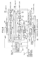
- FIG. 1 shows the configuration of an essential section of a CD-R/RW drive (a disc drive unit capable of writing to and reading from a CD-R disc and a CD-RW disc) to which the present invention has been applied.
- the CD-R/RW drive is designed to permit read clocks and write clocks to be produced by a single phase-locked poop circuit 60.
- the phase-locked poop circuit 60 is provided with a control loop 66 that passes through a phase comparator 62 and a control loop 68 that passes through a phase comparator 64.
- phase comparator 62 is turned ON and the phase comparator 64 is turned OFF so as to turn ON the control loop 66 and turn OFF the control loop 68, or the phase comparator 62 is turned OFF and the phase comparator 64 is turned ON so as to turn OFF the control loop 66 and turn ON the control loop 68
- the control loop 66 compares the phase of a read signal (EFM signal) read from the CD-R/RW disc with the phase of a signal obtained by dividing, in a predetermined manner, an oscillation clock of a VCO (voltage control oscillator) 70 by a frequency divider 72 constructed by a counter or the like.
- An output of the phase comparison (a phase error output) is supplied to an amplifier 74 where a predetermined gain A1 is imparted thereto, input to a control input terminal of the VCO 70 via an adding point 76 and a loop filter 78, and controlled in the oscillation frequency and phase thereof.
- the read clock as an operating clock, normal reproduction and the reproduction of a read EFM signal at a position before reaching an additional writing position is performed.
- the control loop 68 will be described.
- ATIP information recorded as a pre-recorded signal in advance by FM modulation in a wobble of a pregroove is demodulated by a demodulating circuit, which is not shown, and a synchronization signal included in the demodulated ATIP information (if a synchronization signal is missing, then an interpolation signal produced by counting one cycle of synchronization signal from the preceding synchronization signal) Sync 2 is supplied to the phase comparator 64.
- the phase comparator 64 compares the phase of the ATIP synchronization signal Sync 2 with the phase of the signal obtained by dividing an oscillation clock of the VCO 70 in a predetermined manner by a frequency divider 80 constructed by a counter or the like.
- a predetermined gain A2 is imparted to the phase comparison output by an amplifier 82, and supplied to a control input terminal of the VCO 70 through the intermediary of the adding point 76 and the loop filter 78 to control the oscillation frequency and phase thereof. This causes the VCO 70 to issue a write clock synchronized to the ATIP synchronization signal Sync 2. Using the write clock as an operating clock, a write signal is generated.
- the VCO 70 is controlled first by the control loop 66, reading is begun from a position before the recording end of previous information, and the read signal is reproduced by using the clock issued from the VCO 70.
- a write signal is generated in synchronization with the clock issued from the VCO 70, a laser beam of an optical pickup is modulated by the write signal to begin writing, then the control loop of the VCO 70 is switched to the control loop 68. In this manner, the additional writing is carried out.
- Spindle control is conducted on the basis of the read clock or a wobble signal or the ATIP synchronization signal Sync 2 before the additional writing position is reached, then conducted on the basis of the wobble signal or the ATIP synchronization signal Sync 2 after the additional writing position is reached.
- a spindle motor is phase-locked poop-controlled so that these signals are obtained at predetermined frequencies.
- the dividing ratio of the frequency divider 72 is set to an appropriate value N.
- the oscillation frequency of the VCO 70 is controlled by the control loop 66 so that the standard value thereof is N ⁇ f1 (f1 denotes a bit clock frequency standard value of the read EFM signal) before the additional writing position is reached.
- the frequency of an output signal ⁇ 1 of the frequency divider 72 is f1.
- the frequency of an output signal ⁇ 2 of the frequency divider 80 is f2
- the oscillation frequency of the VCO 70 does not fluctuate.
- the frequency divider 80 is reset at the timing of the ATIP synchronization signal Sync 2 before the control loop is switched from the control loop 66 to the control loop 68.
- a synchronization signal detecting circuit 84 detects a sub code frame synchronization signal Sync 1 from the read EFM signal.
- the sub code frame synchronization signal Sync 1 is allowed to have an error of -2 to +2 EFM frame with respect to an ATIP synchronization signal Sync 2.
- a frequency divider 86 divides an output signal of the frequency divider 72 in accordance with a predetermined manner to produce an interpolation signal of the synchronization signal Sync 1, and counts one cycle of the synchronization signal Sync 1 from the detection timing of the synchronization signal Sync 1 so as to produce an interpolation signal Vsync 1.
- a write signal generator 88 generates a write signal in synchronization with an oscillation clock of the VCO 70.
- a sub code frame synchronization of the write signal generator 88 is reset by the sub code frame synchronization signal Sync 1 detected from the read signal before an additional writing position is reached. After the additional writing position is reached, the write signal generator 88 counts the oscillation clocks of the VCO 70 and produces a sub code frame synchronization by itself. From the write signal generator 88, a synchronization signal Sync 3 indicating the sub code frame synchronization is output.
- a phase comparator 90 compares the phase of the ATIP synchronization signal Sync 2 with the phase of the sub code frame synchronization signal Sync 3 of the write signal generator 88, and slightly changes the dividing ratio M of the frequency divider 80 to gradually reduce the phase difference (at a cycle later than the response time of the control loop 68). This gradually reduces the phase deviation of the sub code frame synchronization signal Sync 3 of the write signal with respect to the ATIP synchronization signal Sync 2 after loop switching is made.
- a control circuit 91 implements control necessary for additional writing on respective constituents when it receives an instruction for additional writing.
- phase-locked poop circuit 60 A specific example of the phase-locked poop circuit 60 is shown in Fig. 4.
- the phase comparator 62 supplies a read EFM signal and a comparison input ⁇ 1 to an exclusive OR circuit 92, and outputs the exclusive logic sum.
- the phase comparator 64 shares the same configuration as that of the phase comparator 62.
- the phase comparators 62 and 64 may alternatively be constructed by flip-flop circuits in place of the configuration shown in Fig. 4.
- the amplifier 74 is formed of transistors 98 (p-channel) and 100 (n-channel) in push-pull connection with constant-current sources 95 and 96 disposed at both ends thereof, and outputs of the phase comparator 62 are respectively input to the gates of the transistors 98 and 100.
- the amplifier 82 shares the same configuration as that of the amplifier 74.
- This sets the gains A1 and A2 of the amplifiers 74 and 82 to A1:A2 f2:f1, compensating for the difference in loop gain between the control loops 66 and 68.
- the outputs of the amplifiers 74 and 82 are subjected to current addition at the adding point 76 before they are supplied to the loop filter 78.
- the loop filter 78 charges a capacitor C2 with a current output of the adding point 76, and applies the charge voltage to the control terminal of the VCO 70 to control the oscillation frequency of the VCO 70.
- a series circuit of a resistor R and a capacitor C1 in the loop filter 78 is a phase compensating circuit.
- This reading causes the phase-locked poop circuit 60 to be phase-locked to the read EFM signal, and the recorded information is reproduced, using the clock generated from the VCO 70 as a read clock (S2).
- the sub code frame synchronization signal Sync 3 of the write signal generated from the write signal generator 88 is reset by the sub code frame synchronization signal Sync 1 detected from the read EFM signal (S3).
- the operation mode is switched to a write mode, and a write signal is generated from the write signal generator 88 in synchronization with an oscillation clock of the VCO 70 to begin writing new information (S4).
- the frequency divider 80 is reset by the first ATIP synchronization signal Sync 2, and the phase of the comparison input ⁇ 2 of the phase comparator 64 is matched to the phase of the ATIP synchronization signal Sync 2 (S5).
- the phase comparator 62 is turned OFF, while the phase comparator 64 is turned ON by the switching signal WG so as to turn the control loop 66 OFF and the control loop 68 ON (S6).
- the frequencies and phases of the ATIP synchronization signal Sync 2 and its comparison input ⁇ 2 are substantially matched, and the loop gains are maintained equal by the switching of the amplifiers A1 and A2. Hence, the disturbance (fluctuations in frequency and phase) of the oscillation clocks of the VCO 70 caused by the switching a control loop will be controlled to a minimum.
- phase of the sub code frame synchronization signal Sync 3 of the write signal and the phase of the ATIP synchronization signal Sync 2 are compared by the phase comparator 90 (S7), and the dividing ratio of the frequency divider 80 is slightly changed according to the phase error to perform phase adjustment at a cycle that is later than the response time of the control loop 68.
- the dividing ratio of the frequency divider 80 is changed from M to M-1 (S8) in order to slightly reduce the cycle of the comparison input ⁇ 2 to cause the oscillation frequency of the VCO 70 to be slightly reduced so as to gradually bring the phase of the sub code frame synchronization signal Sync 3 closer to the phase of the ATIP synchronization signal Sync 2.
- the dividing ratio of the frequency divider 80 is set back to M (S9).
- the dividing ratio of the frequency divider 80 is changed from M to M+1 (S8) in order to slightly prolong the cycle of the comparison input ⁇ 2 to cause the oscillation frequency of the VCO 70 to be slightly increased so as to gradually bring the phase of the sub code frame synchronization signal Sync 3 closer to the phase of the ATIP synchronization signal Sync 2.
- the dividing ratio of the frequency divider 80 is set back to M (S9).
- phase of the sub code frame synchronization signal Sync 3 of the write signal substantially coincides with the phase of the ATIP synchronization signal Sync 2. This completes the processing at the beginning of the additional writing, and the writing of new information immediately follows.
- FIG. 8 shows the configuration of an essential section of a CD-R/RW drive to which the present invention has been applied.
- a read clock producing phase-locked poop circuit 102 and a write clock producing phase-locked poop circuit 104 are separately constructed. According to this configuration, it is possible to design phase-locked poop circuits dedicated for producing read clocks and for producing write clocks, respectively, so that circuits that stably operate can be implemented.
- a phase comparator 106 compares the phase of a read EFM signal read from the CD-R/RW disc and the phase of a signal obtained by dividing, in a predetermined manner, an oscillation clock of a VCO 108 by a frequency divider 111 constructed by a counter or the like.
- An amplifier 113 imparts a predetermined gain A0 to an output of the phase comparison, and the output is supplied to a control input terminal of the VCO 108 through the intermediary of a loop filter 115 to control the oscillation frequency and phase thereof. This causes the VCO 108 to issue a read clock synchronized with a bit clock of the read EFM signal. Using the read clock as an operating clock, normal reproduction and the reproduction of a read EFM signal before reaching an additional writing position are performed.
- the phase-locked poop circuit 104 is provided with a control loop 121 that passes through a phase comparator 117 and a control loop 123 that passes through a phase comparator 119.
- a switching signal WG By a switching signal WG, the phase comparator 117 is turned ON and the phase comparator 119 is turned OFF so as to turn ON the control loop 121 and turn OFF the control loop 123, or the phase comparator 117 is turned OFF and the phase comparator 119 is turned ON so as to turn OFF the control loop 121 and turn ON the control loop 123.
- the control loop 121 will be described.
- the phase comparator 117 compares the phase of a read clock with the phase of a signal obtained by dividing, in a predetermined manner, an oscillation clock of a VCO 125 by a frequency divider 127 constructed by a counter or the like. An output of the phase comparison is supplied to an amplifier 129 where a predetermined gain A1 is imparted thereto, input to a control input terminal of the VCO 125 via an adding point 131 and a loop filter 133, and controlled in the oscillation frequency and phase thereof. This causes the VCO 125 to issue a clock synchronized to the read clock (read clock synchronization clock).
- the control loop 123 will be described.
- ATIP information recorded as a pre-recorded signal in advance by FM modulation in a wobble of a pre-groove is demodulated by a demodulating circuit, which is not shown, and a synchronization signal included in the demodulated ATIP information (if a synchronization signal is missing, then an interpolation signal produced by counting one cycle of synchronization signal from the preceding synchronization signal) Sync 2 is supplied to the phase comparator 119.
- the phase comparator 119 compares the phase of the ATIP synchronization signal Sync 2 with the phase of a signal ⁇ 2 obtained by dividing an oscillation clock of the VCO 125 in a predetermined manner by a frequency divider 135 constructed by a counter or the like.
- a predetermined gain A2 is imparted to the phase comparison output by an amplifier 137, and supplied to a control input terminal of the VCO 125 through the intermediary of the adding point 131 and the loop filter 133 to control the oscillation frequency and phase thereof. This causes the VCO 125 to issue a write clock synchronized to the ATIP synchronization signal Sync 2. Using the write clock as an operating clock, a write signal is generated.
- the phase-locked poop circuit 104 To perform additional writing, reading is started from a position before the recording end of previous information, and the read signal is reproduced using a read clock issued from the VCO 108 of the phase-locked poop circuit 102.
- the phase-locked poop circuit 104 first controls the VCO 125 by the control loop 121, then causes a write signal generator 143 to generate a write signal in synchronization with a clock, which is issued from the VCO 125, at a timing when the read position reaches the recording end of the previous information.
- a laser beam of an optical pickup is modulated by the write signal to start writing, then the control of the VCO 125 is switched to the control by the control loop 123. In this manner, the additional writing is performed.
- Spindle control is carried out on the basis of the read clock or a wobble signal or the ATIP synchronization signal Sync 2 before the additional writing position is reached, then carried out on the basis of the wobble signal or the ATIP synchronization signal Sync 2 after the additional writing position is reached.
- a spindle motor is phase-locked poop-controlled so that these signals are obtained at predetermined frequencies.
- the dividing ratios of the frequency dividers 111 and 127 are set to appropriate values N and P, respectively.
- the oscillation frequency of the VCO 125 is controlled by the control loop 121 so that the standard value is N ⁇ P ⁇ f1 (f1 denotes a bit clock frequency standard value of the read EFM signal).
- the frequency of an output signal ⁇ 1 of the frequency divider 127 is N ⁇ f1.
- a dividing ratio M of a frequency divider 135 is set such that the oscillation frequency of the VCO 125 does not fluctuate when switching between the control loops is made.
- the frequency divider 135 is reset at the timing of the ATIP synchronization signal Sync 2 before the control loop of the phase-locked poop circuit 104 is switched from the control loop 121 to the control loop 123.
- an increase in the phase comparison output of the phase comparator 119 will be restrained, thus restraining the fluctuation in the frequency and phase of the oscillation clocks of the VCO 125.
- a synchronization signal detecting circuit 139 detects a sub code frame synchronization signal Sync 1 from the read EFM signal.
- a frequency divider 141 divides an output signal of the frequency divider 111 in accordance with a predetermined manner to produce an interpolation signal of the synchronization signal Sync 1, and counts one cycle of the synchronization signal Sync 1 from the detection timing of the synchronization signal Sync 1 so as to produce an interpolation signal Vsync 1.
- a write signal generator 143 generates a write signal in synchronization with an oscillation clock of the VCO 125.
- a sub code frame synchronization of the write signal generator 143 is reset by the sub code frame synchronization signal Sync 1 detected from the read EFM signal before an additional writing position is reached.
- the write signal generator 143 counts the oscillation clocks of the VCO 125 and produces a sub code frame synchronization by itself. From the write signal generator 143, a synchronization signal Sync 3 indicating the sub code frame synchronization is output.
- a phase comparator 145 compares the phase of the ATIP synchronization signal Sync 2 with the phase of the sub code frame synchronization signal Sync 3 of the write signal generator 143, and slightly changes the dividing ratio M of the frequency divider 135 to gradually reduce the phase difference (at a cycle later than the response time of the control loop 123).
- the phase-locked poop circuit 104 may be constructed in the same manner as shown in, for example, Fig. 4.
- a control circuit 146 implements control necessary for additional writing on respective constituents when it receives an instruction for additional writing.
- the operation for the additional writing under the control of the control circuit 146 may be performed in the same manner as shown by the flowchart of Fig. 6 and the time chart of Fig. 7 described above ⁇ however, in Fig. 7, "phase-locked poop circuit 60" should read “phase-locked poop circuit 104", "Control loop 66” should read “Control loop 121", “Control loop 68” should read “Control loop 123" in (g), and “Frequency divider 80" should read “Frequency divider 135" in (h) ⁇ .
- FIG. 9 shows the configuration of an essential section of a CD-R/RW drive to which the present invention has been applied.
- a read clock producing phase-locked poop circuit 147 and a write clock producing phase-locked poop circuit 149 are separately constructed.
- the write clock producing phase-locked poop circuit 149 has one control loop, and the input of its phase comparator 151 is switched.
- a phase comparator 153 compares the phase of a read EFM signal read from the CD-R/RW disc and the phase of a signal obtained by dividing, in a predetermined manner, an oscillation clock of a VCO 161 by a frequency divider 155 constructed by a counter or the like.
- An amplifier 157 imparts a predetermined gain A0 to an output of the phase comparison, and the output is supplied to a control input terminal of the VCO 161 through the intermediary of a loop filter 159 to control the oscillation frequency and phase thereof. This causes the VCO 161 to issue a read clock synchronized with a bit clock of the read signal. Using the read clock as an operating clock, normal reproduction and the reproduction of a read signal before reaching an additional writing position are performed.
- a frequency divider 163 divides a read clock in a predetermined manner.
- a selector 165 switches between an output signal of the frequency divider 163 and an ATIP synchronization signal Sync 2 by a switching signal WG, and applies it to a phase comparator 151. More specifically, the output signal of the frequency divider 163 is selected before the additional writing position is reached, while the ATIP synchronization signal Sync 2 (if the synchronization signal is missing, then an interpolation signal produced by counting one cycle of synchronization signal from the preceding synchronization signal) is selected and supplied to the phase comparator 151 after the additional writing position is reached.
- the phase comparator 151 compares the phase of the signal selected by the selector 165 and the phase of the signal obtained by dividing, in a predetermined manner, the oscillation clock of a VCO 167 by a frequency divider 169 constructed by a counter or the like.
- a predetermined gain A1 is imparted to the phase comparison output by an amplifier 171, and supplied to a control input terminal of the VCO 167 through the intermediary of a loop filter 173 to control the oscillation frequency and phase thereof. This causes the VCO 167 to issue a write clock synchronized to the signal selected by the selector 165.
- the write clock as an operating clock, a write signal is generated.
- phase-locked poop circuit 149 To perform additional writing, reading is started from a position before the recording end of previous information, and the read signal is reproduced using a read clock issued from the VCO 161 of the phase-locked poop circuit 147.
- the phase-locked poop circuit 149 first selects the output signal of the frequency divider 163 by the selector 165 as the input to the phase comparator 151, then generates a write signal in synchronization with a clock, which is issued from the VCO 167, at a timing when the read position reaches the recording end of the previous information.
- a laser beam of an optical pickup is modulated by the write signal to start writing, then the input to the phase comparator 151 is switched by the selector 165 to the ATIP synchronization signal Sync 2.
- Spindle control is carried out on the basis of the read clock or a wobble signal or the ATIP synchronization signal Sync 2 before the additional writing position is reached, then carried out on the basis of the wobble signal or the ATIP synchronization signal Sync 2 after the additional writing position is reached.
- a spindle motor is phase-locked poop-controlled so that these signals are obtained at predetermined frequencies.
- the dividing ratios of the frequency dividers 155 and 169 are set to appropriate values N and M, respectively.
- the oscillation frequency of the VCO 161 is controlled to N ⁇ f1
- the oscillation clock of the VCO 161 is supplied to the frequency divider 163.
- a dividing ratio P of the frequency divider 163 is set to N ⁇ f1/f2 so that its division output is equal to a frequency standard value f2 of the ATIP synchronization signal Sync 2.
- the oscillation frequency of the VCO 167 does not fluctuate when the output of the selector 165 is switched from the output of the frequency divider 163 to the ATIP synchronization signal Sync 2 at the additional writing position.
- the frequency divider 169 is reset at the timing of the ATIP synchronization signal Sync 2.
- a synchronization signal detecting circuit 175 detects a sub code frame synchronization signal Sync 1 from the read EFM signal.
- a frequency divider 177 divides, in a predetermined manner, an output signal of the frequency divider 155 to produce an interpolation signal of the synchronization signal Sync 1, and counts one cycle of the synchronization signal Sync 1 from the detection timing of the synchronization signal Sync 1 so as to produce an interpolation signal Vsync 1.
- a write signal generator 179 generates a write signal in synchronization with an oscillation clock of the VCO 167.
- a sub code frame synchronization of the write signal generator 179 is reset by the sub code frame synchronization signal Sync 1 detected from the read EFM signal before an additional writing position is reached.
- the write signal generator 179 counts the oscillation clocks of the VCO 167 and produces a sub code frame synchronization by itself. From the write signal generator 179, a synchronization signal Sync 3 indicating the sub code frame synchronization is output.
- a phase comparator 181 compares the phase of the ATIP synchronization signal Sync 2 with the phase of the sub code frame synchronization signal Sync 3 of the write signal generator 179, and slightly changes the dividing ratio M of the frequency divider 169 to gradually reduce the phase difference (at a cycle later than the response time of the phase-locked poop circuit 149). This gradually reduces the phase deviation of the sub code frame synchronization signal Sync 3 of the write signal with respect to the ATIP synchronization signal Sync 2 after loop switching is made.
- a control circuit 183 implements control necessary for additional writing on respective constituents when it receives an instruction for additional writing.
- the operation for the additional writing under the control of the control circuit 183 may be performed in the same manner as shown by the flowchart of Fig. 6 and the time chart of Fig. 7 described above ⁇ however, in Fig. 7, "Loop used in phase-locked poop circuit 60" should read “Selection by the selector 165", "Control loop 66" should read “Output of the frequency divider 163", and “Control loop 68" should read “ATIP synchronization signal Sync 2" in (g), and “Frequency divider 80" should read “Frequency divider 169" in (h) ⁇ .
- the present invention can be also applied to the recording in various types of DVD discs, including DVD-Rs, DVD-RAMs, DVD-RWs, and DVD+RWs, and a variety of types of recording media, such as magneto-optical discs, magnetic discs, and magnetic tapes in which pre-recorded signals have been recorded in advance along recording tracks.
- the pre-pits formed in advance along a recording track correspond to pre-recorded signals.
Landscapes
- Engineering & Computer Science (AREA)
- Signal Processing (AREA)
- Signal Processing For Digital Recording And Reproducing (AREA)
- Synchronisation In Digital Transmission Systems (AREA)
- Stabilization Of Oscillater, Synchronisation, Frequency Synthesizers (AREA)
Applications Claiming Priority (2)
| Application Number | Priority Date | Filing Date | Title |
|---|---|---|---|
| JP2001057811A JP4487433B2 (ja) | 2001-03-02 | 2001-03-02 | 記録媒体記録装置 |
| JP2001057811 | 2001-03-02 |
Publications (3)
| Publication Number | Publication Date |
|---|---|
| EP1237158A2 true EP1237158A2 (fr) | 2002-09-04 |
| EP1237158A3 EP1237158A3 (fr) | 2006-11-02 |
| EP1237158B1 EP1237158B1 (fr) | 2014-05-07 |
Family
ID=18917631
Family Applications (1)
| Application Number | Title | Priority Date | Filing Date |
|---|---|---|---|
| EP02004881.5A Expired - Lifetime EP1237158B1 (fr) | 2001-03-02 | 2002-03-04 | Méthode d'écriture consécutif dans un disque enregistrable |
Country Status (4)
| Country | Link |
|---|---|
| US (1) | US6909678B2 (fr) |
| EP (1) | EP1237158B1 (fr) |
| JP (1) | JP4487433B2 (fr) |
| CN (1) | CN1254816C (fr) |
Families Citing this family (25)
| Publication number | Priority date | Publication date | Assignee | Title |
|---|---|---|---|---|
| JP3969042B2 (ja) * | 2001-09-28 | 2007-08-29 | ヤマハ株式会社 | 光ディスク記録装置 |
| US20030206501A1 (en) | 2002-05-02 | 2003-11-06 | Hubert Song | Method and apparatus for providing high speed recording on an optical medium |
| US7133348B2 (en) * | 2002-08-01 | 2006-11-07 | Mediatek Inc. | Phase lock loop for a controller in an optical disk system and methods therefor |
| TWI298156B (en) * | 2002-10-24 | 2008-06-21 | Tian Holdings Llc | Discrimination method for light storage device |
| JP2004253057A (ja) * | 2003-02-20 | 2004-09-09 | Sanyo Electric Co Ltd | クロック生成装置 |
| JP4445206B2 (ja) * | 2003-03-10 | 2010-04-07 | 株式会社東芝 | ディスク記録再生装置 |
| TWI316702B (en) * | 2003-09-15 | 2009-11-01 | Tian Holdings Llc | Discriminating method of an optical disc device for ascertaining the format of an loaded optical disc |
| US20050226114A1 (en) | 2004-03-31 | 2005-10-13 | Stanley Liow | Method and apparatus for generating absolute time in pregroove data |
| JP4077396B2 (ja) * | 2003-11-19 | 2008-04-16 | 株式会社東芝 | ディスク装置及びディスク再生方法 |
| US7570561B2 (en) * | 2004-05-25 | 2009-08-04 | Bryan Tai | Method for determining type of digital versatile discs |
| US7626907B2 (en) * | 2004-05-25 | 2009-12-01 | Ricky Chang | Method and apparatus for determining type of digital versatile disc |
| US7746745B2 (en) * | 2004-05-25 | 2010-06-29 | Ricky Chang | Method for determining the type of digital versatile disc |
| US7248549B2 (en) * | 2004-07-30 | 2007-07-24 | Agere Systems Inc. | System for locking a clock onto the frequency of data recorded on a storage medium |
| JP2006318617A (ja) * | 2005-05-16 | 2006-11-24 | Sony Corp | 基準クロック生成回路及び記録媒体記録装置 |
| US20070064566A1 (en) * | 2005-09-21 | 2007-03-22 | Wei-Hsin Hsu | Signal process device and method for obtaining wobble signal |
| US20070127343A1 (en) * | 2005-12-05 | 2007-06-07 | Wei-Hsiang Tseng | Information recording device and related method |
| WO2008063199A1 (fr) * | 2006-11-20 | 2008-05-29 | Rambus Inc. | Systèmes mémoires et procédés pour ajuster de façon dynamique la phase d'un signal d'échantillonnage de lecture et données représentant une dérive d'horloge reçue |
| US10014026B1 (en) | 2017-06-20 | 2018-07-03 | Seagate Technology Llc | Head delay calibration and tracking in MSMR systems |
| CN109031429B (zh) * | 2018-05-29 | 2020-04-10 | 福州华虹智能科技股份有限公司 | 一种吸收相位差检测方法及系统 |
| US11016681B1 (en) | 2018-07-31 | 2021-05-25 | Seagate Technology Llc | Multi-threshold parameter adaptation |
| US11018842B1 (en) | 2018-07-31 | 2021-05-25 | Seagate Technology Llc | Dynamic timing recovery bandwidth modulation for phase offset mitigation |
| US10803902B1 (en) | 2018-08-19 | 2020-10-13 | Seagate Technology Llc | Hardware-based read sample averaging |
| US10468060B1 (en) | 2018-09-27 | 2019-11-05 | Seagate Technology Llc | Cancelling adjacent track interference |
| CN113050718B (zh) * | 2021-04-25 | 2025-12-16 | 国能(北京)电气技术有限公司 | 风电变流器数字化温湿度检测控制系统 |
| US11735220B2 (en) | 2021-12-27 | 2023-08-22 | Seagate Technology Llc | Phase locking multiple clocks of different frequencies |
Citations (1)
| Publication number | Priority date | Publication date | Assignee | Title |
|---|---|---|---|---|
| EP0930617A2 (fr) | 1998-01-14 | 1999-07-21 | Pioneer Electronic Corporation | Appareil d'enregistrement d'information pour support d'enregistrement réinscriptible |
Family Cites Families (6)
| Publication number | Priority date | Publication date | Assignee | Title |
|---|---|---|---|---|
| JPH0756746B2 (ja) * | 1985-03-29 | 1995-06-14 | ソニー株式会社 | 追記型光デイスクにおける記録済デ−タの目録作成方法 |
| JP4102483B2 (ja) * | 1998-06-02 | 2008-06-18 | パイオニア株式会社 | 情報記録装置 |
| JP3163064B2 (ja) * | 1998-07-22 | 2001-05-08 | 三洋電機株式会社 | ディスク記録装置 |
| JP3755714B2 (ja) * | 1998-12-09 | 2006-03-15 | 株式会社リコー | 情報記録方式 |
| JP2000251405A (ja) * | 1999-02-26 | 2000-09-14 | Sanyo Electric Co Ltd | ディスク記録装置 |
| JP3877479B2 (ja) * | 1999-11-29 | 2007-02-07 | 三洋電機株式会社 | ディスク記録装置 |
-
2001
- 2001-03-02 JP JP2001057811A patent/JP4487433B2/ja not_active Expired - Fee Related
-
2002
- 2002-03-01 US US10/086,276 patent/US6909678B2/en not_active Expired - Lifetime
- 2002-03-04 CN CNB021067244A patent/CN1254816C/zh not_active Expired - Fee Related
- 2002-03-04 EP EP02004881.5A patent/EP1237158B1/fr not_active Expired - Lifetime
Patent Citations (1)
| Publication number | Priority date | Publication date | Assignee | Title |
|---|---|---|---|---|
| EP0930617A2 (fr) | 1998-01-14 | 1999-07-21 | Pioneer Electronic Corporation | Appareil d'enregistrement d'information pour support d'enregistrement réinscriptible |
Also Published As
| Publication number | Publication date |
|---|---|
| JP2002260333A (ja) | 2002-09-13 |
| EP1237158B1 (fr) | 2014-05-07 |
| US6909678B2 (en) | 2005-06-21 |
| EP1237158A3 (fr) | 2006-11-02 |
| JP4487433B2 (ja) | 2010-06-23 |
| US20030198152A1 (en) | 2003-10-23 |
| CN1254816C (zh) | 2006-05-03 |
| CN1374655A (zh) | 2002-10-16 |
Similar Documents
| Publication | Publication Date | Title |
|---|---|---|
| EP1237158B1 (fr) | Méthode d'écriture consécutif dans un disque enregistrable | |
| US7012864B2 (en) | Optical disk recorder for writing data with variable density | |
| JPH1173645A (ja) | 光ディスク装置 | |
| US6125089A (en) | Recording timing control circuit for optical disk driving device | |
| JP2000298842A (ja) | 記録可能型clv方式光ディスクおよびその記録装置 | |
| US6775211B1 (en) | System and method for disk recording | |
| KR100502461B1 (ko) | 위상동기루프회로및이것이내장된재생장치 | |
| JPH1098377A (ja) | Pll回路 | |
| JPH10257041A (ja) | フェイズロックドループ回路及び再生装置 | |
| JP3605023B2 (ja) | クロック生成回路 | |
| US6992958B2 (en) | Phase-locked loop circuit for reproducing a channel clock | |
| JPH11317018A (ja) | ディスク再生装置及びrfアンプ制御回路 | |
| JPH09120584A (ja) | 光ディスク、光ディスク記録再生装置、光ディスク記録再生方法、光ディスク形成装置、および光ディスク形成方法 | |
| US7397751B2 (en) | Optical disk apparatus, method of recording information, and information recording medium | |
| JP2004178743A (ja) | 光ディスク記録装置 | |
| JPH09115238A (ja) | マルチ倍速の光ディスク再生装置のスピンドルサーボ回路 | |
| JP2003059184A (ja) | Dvd−rおよびdvd−rwにおける記録位置ずれ補正方法およびその装置 | |
| JP4494941B2 (ja) | データ記録用クロック信号発生回路 | |
| JP2002230757A (ja) | クロック生成回路及びそれを用いた記録再生装置 | |
| JPH05183431A (ja) | 位相同期回路 | |
| JPH08149418A (ja) | ディスク再生装置の同期信号検出装置 | |
| JP2001274683A (ja) | 信号発生装置及び再生装置 | |
| JPH05182356A (ja) | 情報記録再生装置の位相同期回路 | |
| JP2002352434A (ja) | 記録再生装置、および記録再生方法 | |
| JP2003157537A (ja) | 光ディスク駆動装置 |
Legal Events
| Date | Code | Title | Description |
|---|---|---|---|
| PUAI | Public reference made under article 153(3) epc to a published international application that has entered the european phase |
Free format text: ORIGINAL CODE: 0009012 |
|
| AK | Designated contracting states |
Kind code of ref document: A2 Designated state(s): AT BE CH CY DE DK ES FI FR GB GR IE IT LI LU MC NL PT SE TR |
|
| AX | Request for extension of the european patent |
Free format text: AL;LT;LV;MK;RO;SI |
|
| PUAL | Search report despatched |
Free format text: ORIGINAL CODE: 0009013 |
|
| AK | Designated contracting states |
Kind code of ref document: A3 Designated state(s): AT BE CH CY DE DK ES FI FR GB GR IE IT LI LU MC NL PT SE TR |
|
| AX | Request for extension of the european patent |
Extension state: AL LT LV MK RO SI |
|
| RIC1 | Information provided on ipc code assigned before grant |
Ipc: G11B 27/24 20060101ALI20060922BHEP Ipc: G11B 20/14 20060101AFI20020620BHEP Ipc: G11B 27/30 20060101ALI20060922BHEP Ipc: G11B 27/19 20060101ALI20060922BHEP Ipc: G11B 20/10 20060101ALI20060922BHEP |
|
| 17P | Request for examination filed |
Effective date: 20070502 |
|
| RAP1 | Party data changed (applicant data changed or rights of an application transferred) |
Owner name: YAMAHA CORPORATION |
|
| AKX | Designation fees paid |
Designated state(s): DE FR GB |
|
| 17Q | First examination report despatched |
Effective date: 20100119 |
|
| GRAP | Despatch of communication of intention to grant a patent |
Free format text: ORIGINAL CODE: EPIDOSNIGR1 |
|
| INTG | Intention to grant announced |
Effective date: 20131114 |
|
| GRAS | Grant fee paid |
Free format text: ORIGINAL CODE: EPIDOSNIGR3 |
|
| GRAA | (expected) grant |
Free format text: ORIGINAL CODE: 0009210 |
|
| AK | Designated contracting states |
Kind code of ref document: B1 Designated state(s): DE FR GB |
|
| REG | Reference to a national code |
Ref country code: GB Ref legal event code: FG4D |
|
| REG | Reference to a national code |
Ref country code: DE Ref legal event code: R096 Ref document number: 60246249 Country of ref document: DE Effective date: 20140612 |
|
| REG | Reference to a national code |
Ref country code: DE Ref legal event code: R097 Ref document number: 60246249 Country of ref document: DE |
|
| PLBE | No opposition filed within time limit |
Free format text: ORIGINAL CODE: 0009261 |
|
| STAA | Information on the status of an ep patent application or granted ep patent |
Free format text: STATUS: NO OPPOSITION FILED WITHIN TIME LIMIT |
|
| 26N | No opposition filed |
Effective date: 20150210 |
|
| REG | Reference to a national code |
Ref country code: DE Ref legal event code: R097 Ref document number: 60246249 Country of ref document: DE Effective date: 20150210 |
|
| REG | Reference to a national code |
Ref country code: FR Ref legal event code: PLFP Year of fee payment: 15 |
|
| REG | Reference to a national code |
Ref country code: FR Ref legal event code: PLFP Year of fee payment: 16 |
|
| REG | Reference to a national code |
Ref country code: FR Ref legal event code: PLFP Year of fee payment: 17 |
|
| PGFP | Annual fee paid to national office [announced via postgrant information from national office to epo] |
Ref country code: DE Payment date: 20180220 Year of fee payment: 17 Ref country code: GB Payment date: 20180228 Year of fee payment: 17 |
|
| PGFP | Annual fee paid to national office [announced via postgrant information from national office to epo] |
Ref country code: FR Payment date: 20180111 Year of fee payment: 17 |
|
| REG | Reference to a national code |
Ref country code: DE Ref legal event code: R119 Ref document number: 60246249 Country of ref document: DE |
|
| GBPC | Gb: european patent ceased through non-payment of renewal fee |
Effective date: 20190304 |
|
| PG25 | Lapsed in a contracting state [announced via postgrant information from national office to epo] |
Ref country code: GB Free format text: LAPSE BECAUSE OF NON-PAYMENT OF DUE FEES Effective date: 20190304 Ref country code: DE Free format text: LAPSE BECAUSE OF NON-PAYMENT OF DUE FEES Effective date: 20191001 |
|
| PG25 | Lapsed in a contracting state [announced via postgrant information from national office to epo] |
Ref country code: FR Free format text: LAPSE BECAUSE OF NON-PAYMENT OF DUE FEES Effective date: 20190331 |