EP1215698B1 - Plasmabildschirm mit Leuchtstoffschicht - Google Patents
Plasmabildschirm mit Leuchtstoffschicht Download PDFInfo
- Publication number
- EP1215698B1 EP1215698B1 EP01000719A EP01000719A EP1215698B1 EP 1215698 B1 EP1215698 B1 EP 1215698B1 EP 01000719 A EP01000719 A EP 01000719A EP 01000719 A EP01000719 A EP 01000719A EP 1215698 B1 EP1215698 B1 EP 1215698B1
- Authority
- EP
- European Patent Office
- Prior art keywords
- phosphor
- color
- plasma
- phosphors
- picture screen
- Prior art date
- Legal status (The legal status is an assumption and is not a legal conclusion. Google has not performed a legal analysis and makes no representation as to the accuracy of the status listed.)
- Expired - Lifetime
Links
- OAICVXFJPJFONN-UHFFFAOYSA-N Phosphorus Chemical compound [P] OAICVXFJPJFONN-UHFFFAOYSA-N 0.000 claims description 85
- 239000010410 layer Substances 0.000 claims description 44
- 229910052727 yttrium Inorganic materials 0.000 claims description 32
- 229910052688 Gadolinium Inorganic materials 0.000 claims description 24
- 239000008241 heterogeneous mixture Substances 0.000 claims description 20
- 239000011521 glass Substances 0.000 claims description 15
- 210000004180 plasmocyte Anatomy 0.000 claims description 10
- 229910052771 Terbium Inorganic materials 0.000 claims description 8
- 229910052693 Europium Inorganic materials 0.000 claims description 6
- 239000011241 protective layer Substances 0.000 claims description 6
- 238000003491 array Methods 0.000 claims description 3
- 229910002248 LaBO3 Inorganic materials 0.000 claims 1
- 229910001477 LaPO4 Inorganic materials 0.000 claims 1
- 229910009372 YVO4 Inorganic materials 0.000 claims 1
- 229910052844 willemite Inorganic materials 0.000 claims 1
- 239000011572 manganese Substances 0.000 description 23
- 239000011701 zinc Substances 0.000 description 22
- 229910004283 SiO 4 Inorganic materials 0.000 description 21
- 238000007650 screen-printing Methods 0.000 description 17
- 239000011230 binding agent Substances 0.000 description 16
- 229910052720 vanadium Inorganic materials 0.000 description 11
- 239000007789 gas Substances 0.000 description 10
- 239000000203 mixture Substances 0.000 description 8
- 239000003086 colorant Substances 0.000 description 7
- 229910052725 zinc Inorganic materials 0.000 description 7
- 229910052684 Cerium Inorganic materials 0.000 description 6
- 238000000576 coating method Methods 0.000 description 6
- 238000000034 method Methods 0.000 description 5
- 239000000654 additive Substances 0.000 description 4
- 239000012298 atmosphere Substances 0.000 description 4
- QVGXLLKOCUKJST-UHFFFAOYSA-N atomic oxygen Chemical compound [O] QVGXLLKOCUKJST-UHFFFAOYSA-N 0.000 description 4
- 230000005284 excitation Effects 0.000 description 4
- 229910052760 oxygen Inorganic materials 0.000 description 4
- 239000001301 oxygen Substances 0.000 description 4
- 238000007669 thermal treatment Methods 0.000 description 4
- 239000011248 coating agent Substances 0.000 description 3
- 238000010276 construction Methods 0.000 description 3
- 229910052756 noble gas Inorganic materials 0.000 description 3
- 230000005855 radiation Effects 0.000 description 3
- 241001167556 Catena Species 0.000 description 2
- 229910002420 LaOCl Inorganic materials 0.000 description 2
- -1 LaPO 4 : Ce Chemical class 0.000 description 2
- 229920000388 Polyphosphate Polymers 0.000 description 2
- 230000004888 barrier function Effects 0.000 description 2
- 230000015556 catabolic process Effects 0.000 description 2
- 210000004027 cell Anatomy 0.000 description 2
- 238000006731 degradation reaction Methods 0.000 description 2
- 229910052748 manganese Inorganic materials 0.000 description 2
- 238000004519 manufacturing process Methods 0.000 description 2
- 230000003647 oxidation Effects 0.000 description 2
- 238000007254 oxidation reaction Methods 0.000 description 2
- 239000001205 polyphosphate Substances 0.000 description 2
- 235000011176 polyphosphates Nutrition 0.000 description 2
- PWHULOQIROXLJO-UHFFFAOYSA-N Manganese Chemical compound [Mn] PWHULOQIROXLJO-UHFFFAOYSA-N 0.000 description 1
- 229910004298 SiO 2 Inorganic materials 0.000 description 1
- HCHKCACWOHOZIP-UHFFFAOYSA-N Zinc Chemical compound [Zn] HCHKCACWOHOZIP-UHFFFAOYSA-N 0.000 description 1
- 229910052784 alkaline earth metal Inorganic materials 0.000 description 1
- 150000001342 alkaline earth metals Chemical class 0.000 description 1
- 150000004645 aluminates Chemical class 0.000 description 1
- 239000002518 antifoaming agent Substances 0.000 description 1
- 230000015572 biosynthetic process Effects 0.000 description 1
- 229910052793 cadmium Inorganic materials 0.000 description 1
- BDOSMKKIYDKNTQ-UHFFFAOYSA-N cadmium atom Chemical compound [Cd] BDOSMKKIYDKNTQ-UHFFFAOYSA-N 0.000 description 1
- 239000004020 conductor Substances 0.000 description 1
- 238000000354 decomposition reaction Methods 0.000 description 1
- 239000003989 dielectric material Substances 0.000 description 1
- 238000002845 discoloration Methods 0.000 description 1
- 239000002270 dispersing agent Substances 0.000 description 1
- 238000010410 dusting Methods 0.000 description 1
- 238000004924 electrostatic deposition Methods 0.000 description 1
- 238000011049 filling Methods 0.000 description 1
- 229910052734 helium Inorganic materials 0.000 description 1
- 229910052743 krypton Inorganic materials 0.000 description 1
- 239000007791 liquid phase Substances 0.000 description 1
- 229910052751 metal Inorganic materials 0.000 description 1
- 239000002184 metal Substances 0.000 description 1
- 229910052754 neon Inorganic materials 0.000 description 1
- 239000003960 organic solvent Substances 0.000 description 1
- 238000002360 preparation method Methods 0.000 description 1
- 238000004062 sedimentation Methods 0.000 description 1
- 239000000126 substance Substances 0.000 description 1
- 239000004094 surface-active agent Substances 0.000 description 1
- 239000000725 suspension Substances 0.000 description 1
- XLYOFNOQVPJJNP-UHFFFAOYSA-N water Substances O XLYOFNOQVPJJNP-UHFFFAOYSA-N 0.000 description 1
- 229910052724 xenon Inorganic materials 0.000 description 1
- FHNFHKCVQCLJFQ-UHFFFAOYSA-N xenon atom Chemical compound [Xe] FHNFHKCVQCLJFQ-UHFFFAOYSA-N 0.000 description 1
Images

Classifications
-
- C—CHEMISTRY; METALLURGY
- C09—DYES; PAINTS; POLISHES; NATURAL RESINS; ADHESIVES; COMPOSITIONS NOT OTHERWISE PROVIDED FOR; APPLICATIONS OF MATERIALS NOT OTHERWISE PROVIDED FOR
- C09K—MATERIALS FOR MISCELLANEOUS APPLICATIONS, NOT PROVIDED FOR ELSEWHERE
- C09K11/00—Luminescent, e.g. electroluminescent, chemiluminescent materials
- C09K11/08—Luminescent, e.g. electroluminescent, chemiluminescent materials containing inorganic luminescent materials
- C09K11/77—Luminescent, e.g. electroluminescent, chemiluminescent materials containing inorganic luminescent materials containing rare earth metals
- C09K11/7728—Luminescent, e.g. electroluminescent, chemiluminescent materials containing inorganic luminescent materials containing rare earth metals containing europium
- C09K11/7734—Aluminates
-
- C—CHEMISTRY; METALLURGY
- C09—DYES; PAINTS; POLISHES; NATURAL RESINS; ADHESIVES; COMPOSITIONS NOT OTHERWISE PROVIDED FOR; APPLICATIONS OF MATERIALS NOT OTHERWISE PROVIDED FOR
- C09K—MATERIALS FOR MISCELLANEOUS APPLICATIONS, NOT PROVIDED FOR ELSEWHERE
- C09K11/00—Luminescent, e.g. electroluminescent, chemiluminescent materials
- C09K11/08—Luminescent, e.g. electroluminescent, chemiluminescent materials containing inorganic luminescent materials
- C09K11/77—Luminescent, e.g. electroluminescent, chemiluminescent materials containing inorganic luminescent materials containing rare earth metals
- C09K11/7715—Luminescent, e.g. electroluminescent, chemiluminescent materials containing inorganic luminescent materials containing rare earth metals containing cerium
- C09K11/7726—Borates
-
- C—CHEMISTRY; METALLURGY
- C09—DYES; PAINTS; POLISHES; NATURAL RESINS; ADHESIVES; COMPOSITIONS NOT OTHERWISE PROVIDED FOR; APPLICATIONS OF MATERIALS NOT OTHERWISE PROVIDED FOR
- C09K—MATERIALS FOR MISCELLANEOUS APPLICATIONS, NOT PROVIDED FOR ELSEWHERE
- C09K11/00—Luminescent, e.g. electroluminescent, chemiluminescent materials
- C09K11/08—Luminescent, e.g. electroluminescent, chemiluminescent materials containing inorganic luminescent materials
- C09K11/77—Luminescent, e.g. electroluminescent, chemiluminescent materials containing inorganic luminescent materials containing rare earth metals
- C09K11/7766—Luminescent, e.g. electroluminescent, chemiluminescent materials containing inorganic luminescent materials containing rare earth metals containing two or more rare earth metals
- C09K11/778—Borates
-
- H—ELECTRICITY
- H01—ELECTRIC ELEMENTS
- H01J—ELECTRIC DISCHARGE TUBES OR DISCHARGE LAMPS
- H01J11/00—Gas-filled discharge tubes with alternating current induction of the discharge, e.g. alternating current plasma display panels [AC-PDP]; Gas-filled discharge tubes without any main electrode inside the vessel; Gas-filled discharge tubes with at least one main electrode outside the vessel
- H01J11/20—Constructional details
- H01J11/34—Vessels, containers or parts thereof, e.g. substrates
- H01J11/42—Fluorescent layers
-
- H—ELECTRICITY
- H01—ELECTRIC ELEMENTS
- H01J—ELECTRIC DISCHARGE TUBES OR DISCHARGE LAMPS
- H01J2211/00—Plasma display panels with alternate current induction of the discharge, e.g. AC-PDPs
- H01J2211/20—Constructional details
- H01J2211/34—Vessels, containers or parts thereof, e.g. substrates
- H01J2211/42—Fluorescent layers
Definitions
- the application relates to a plasma display panel equipped with a front panel having a glass plate on which a dielectric layer and a protective layer are applied, having a support plate provided with a phosphor layer, with a rib structure defining the space between the front plate and the support plate in plasma cells are filled with a gas, divides, and with one or more electrode arrays on the front panel and the support plate for generating silent electrical discharges in the plasma cells.
- Plasma screens enable color images with high resolution, large screen diagonal and are of compact design.
- a plasma display panel has a hermetically sealed glass cell filled with a gas with lattice-shaped electrodes. By applying an electric voltage, a gas discharge is produced, which generates light in the ultraviolet range. With phosphors, this light can be converted into visible light and emitted through the front panel of the glass cell to the viewer.
- each of the selected phosphors has certain disadvantages that can not be remedied easily.
- the blue phosphor BaMgAl 10 O 17 : Eu shows a strong decrease in brightness due to the irradiation with VUV light.
- the white point of the plasma picture screen shifts toward yellow-orange, since the green and in particular the red phosphor degrades less strongly.
- the green phosphor Zn 2 SiO 4 : Mn has a relatively long decay time of about 10 ms and only a moderate efficiency in the excitation with VUV light. Efficiency continues to decrease significantly as saturation increases with increasing luminance. In addition, its stability upon excitation with VUV light is also lower than that of the red phosphor (Y, Gd) BO 3 : Eu.
- red phosphor (Y, Gd) BO 3 Eu is very efficient upon excitation with VUV light, its color point is less red than that of Y 2 O 2 S: Eu used in cathode ray tubes.
- the phosphors are provided with a coating, for example, or alternative phosphors are synthesized. So is out of the DE 197 27 607
- a blue-emitting aluminate phosphor with a coating of catena polyphosphate of one or more alkaline earth metals, zinc, cadmium and / or manganese known.
- the coating of catena polyphosphate reduces the degradation of the phosphor by excitation with VUV light.
- EP 1 187 167 A1 shows a color screen equipped with a blue phosphor layer comprising a first phosphor having a light emission in the region of 490 nm and a second phosphor having a light emission in the range of 380 to 450 nm , contains. This improves the color temperature.
- a plasma picture screen equipped with a front panel having a glass plate on which a dielectric layer and a protective layer are applied, having a support plate provided with a phosphor layer containing a heterogeneous mixture of at least two phosphors having the same color having a rib structure dividing the space between the faceplate and the support plate into plasma cells filled with a gas, and having one or more electrode arrays on the faceplate and the support plate for generating silent electric discharges in the plasma cells, wherein the phosphor layer is subdivided into different ear segments and at least one color segment contains a heterogeneous mixture of at least two phosphors which emit the same color and one phosphor has a shorter decay time than the other.
- the undesirable properties of the phosphors can be mutually reduced or compensated.
- the phosphor layer of a plasma picture screen contains different color segments, each with a phosphor which emits in one of the colors blue, green or red.
- the properties of this color segment can be improved.
- a color segment of the phosphor layer may also comprise a heterogeneous mixture of (Y, Gd) BO 3 : Eu and a second, red-emitting phosphor whose color point (x, y) has a y value ⁇ 0.36.
- the second, red-emitting phosphor is selected from the group Y 2 O 3 : Eu, YVO 4 : Eu, Y (V, P) O 4 : Eu and (Y 1-x Gd x ) 2 O. 3 : Eu with 0 ⁇ x ⁇ 1.
- Eu 3+ -activated phosphors have a shorter decay time than (Y, Gd) BO 3 : Eu, which also reduces motion artifacts in the image display. Furthermore, it is preferred that a Earbsegment the phosphor layer contains a heterogeneous mixture of Zn 2 SiO 4 Mn and a Tb 3+ -activated phosphor.
- the decrease in the brightness of a green-emitting color segment of a phosphor layer during the lifetime of a plasma picture screen can be reduced because Tb 3+ -activated phosphors have a higher stability than Zn 2 SiO 4 : Mn under irradiation with VUV light.
- Tb 3+ is relatively difficult to oxidize to Tb 4+
- Mn 2+ is very sensitive to oxidation.
- the luminous efficacy, in particular at high luminance a green-emitting Earbsegments the phosphor layer can be increased.
- the color brilliance of a green-emitting Earbsegments is improved by a reduced saturation.
- the Tb 3+ -activated phosphor is chosen from the group of LaPO 4: Ce, Tb, Y 2 SiO 2: Tb, GdMgB 5 O 10: Ce, Tb, CeMgAl 11 O 19: Tb, GdBO 3: Tb, (Y 1 -x Gd x ) BO 3 : Tb where 0 ⁇ x ⁇ 1, YBO 3 : Tb, LaOCl: Tb and InBO 3 : Tb.
- Tb 3+ -activated phosphors have a shorter decay time than Zn 2 SiO 4 : Mn.
- Zn 2 SiO 4 : Mn By a heterogeneous mixture of these Tb 3+ -activated phosphors with Zn 2 SiO 4 : Mn in a green-emitting color segment of the phosphor layer motion artifacts can be reduced in the image display.
- a color segment of the phosphor layer comprises a heterogeneous mixture of BaMgAl 10 O 17 : Eu and a luminophore which contains from the group of the Ce 3+ -activated phosphors and the Tm 3+ -activated phosphors.
- the decrease in the brightness of a blue-emitting phosphor layer or of a blue-emitting color segment of a phosphor layer during the lifetime of a plasma image can be reduced because Ce 3+ -activated phosphors and Tm 3+ -activated phosphors have a higher stability than BaMgAl 10 O 17 : Eu under irradiation with VUV light exhibit.
- the Ce 3+ -activated phosphor is selected from the group YBO 3 : Ce and (Y 1-x Gd x ) BO 3 : Ce with 0 ⁇ x ⁇ 1.
- the Tm 3+ -activated phosphor is LaBO 3 : Tm.
- the color point of a blue-emitting color segment of a phosphor layer can be improved since YBO 3 : Ce, (Y 1-x Gd x ) BO 3 : Ce with 0 ⁇ x ⁇ 1 and LaBO 3 : Tm have a deeper blue emission color than BaMgAl 10 O 17 : Eu.
- a plasma cell of an AC plasma display panel having a coplanar arrangement of the electrodes has a front panel 1 and a support plate 2.
- the front panel 1 includes a glass plate 3, on which a dielectric layer 4 and thereon a protective layer 5 are applied.
- the protective layer 5 is preferably made of MgO, and the dielectric layer 4 is made of, for example, PbO-containing glass.
- the discharge electrodes 6, 7 are made of, for example, metal or ITO.
- the support plate 2 is made of glass and on the support plate 2 are parallel, strip-shaped, perpendicular to the discharge electrodes 6,7 extending address electrodes 10 applied, for example, Ag.
- a phosphor layer 9 which emits light in one of the three primary colors red, green or blue.
- the phosphor layer is divided into several color segments.
- the red, green or blue-emitting color segments of the phosphor layer 9 are applied in the form of vertical strip triplets.
- the individual plasma cells are separated by a rib structure 12 with barrier ribs of preferably dielectric material.
- a gas preferably a noble gas mixture, for example, He, Ne or Kr with Xe as UV-light generating component
- a plasma is formed in the plasma region 8, through which, depending on the composition of the gas, radiation 11 in the UV range, in particular in the VUV range.
- the dielectric layer 4 over the transparent discharge electrodes 6,7 is used, inter alia, in AC plasma screens to prevent a direct discharge between the discharge electrode 6,7 consisting of conductive material and thus the formation of an arc upon ignition of the discharge.
- At least one color segment of the phosphor layer 9 contains a heterogeneous mixture of at least two phosphors.
- a heterogeneous mixture is a heterogeneous aggregate containing at least two substances.
- a blue-emitting color segment of the phosphor layer 9 contains, in addition to BaMgAl 10 O 17 : Eu, a Ce 3+ -activated phosphor or a Tm 3+ -activated phosphor.
- the Ce 3+ -activated phosphor can be selected, for example, from the group YBO 3 : Ce and (Y 1 -x Gd x ) BO 3 : Ce with 0 ⁇ x ⁇ 1 and as Tm 3+ -activated phosphor can, for example, LaBO 3 : Tm be used.
- YBO 3 Ce
- (Y 1 -x Gd x ) BO 3 Ce with 0 ⁇ x ⁇ 1
- LaBO 3 Tm each have a decay time of less than 0.1 ms.
- the x-value of the color point of the three phosphors is ⁇ 0.168, and thus the emission color of these phosphors appears to be deeper blue than that of BaMgAl 10 O 17 : Eu.
- the three phosphors have a high luminous efficacy when excited by VUV light and a higher stability than BaMgAl 10 O 17 : Eu when exposed to VUV light.
- Table 1 Decay times and color points of suitable blue-emitting Ce ⁇ sup> 3 + ⁇ / sup> and Tm ⁇ sup> 3 + ⁇ / sup> activated phosphors fluorescent Cooldown [ms] Color point [x, y] YBO 3 : Ce ⁇ 0.1 0.165, 0.027 (Y 0.5 Gd 0.5 ) BO 3 : Ce ⁇ 0.1 0.168, 0.030 LaBO 3 : Tm ⁇ 0.1 0.168, 0.060
- a green-emitting color segment of the phosphor 9 contains Zn 2 SiO 4 : Mn and a Tb 3+ -activated phosphor such as LaPO 4 : Ce, Tb, Y 2 SiO 5 : Tb, GdMgB 5 O 10 : Ce, Tb, CeMgAl 11 O 19 : Tb, GdBO 3 : Tb, (Y 1-x Gd) BO 3 : Tb where 0 ⁇ x ⁇ 1, YBO 3 : Tb, LaOCl: Tb or InBO 3 : Tb.
- a Tb 3+ -activated phosphor such as LaPO 4 : Ce, Tb, Y 2 SiO 5 : Tb, GdMgB 5 O 10 : Ce, Tb, CeMgAl 11 O 19 : Tb, GdBO 3 : Tb, (Y 1-x Gd) BO 3 : Tb where 0 ⁇ x ⁇ 1, YBO 3 : Tb, LaOCl: Tb or
- Tb As shown in Table 2, except for InBO 3 : Tb, all of the selected Tb 3+ -activated phosphors have a shorter decay time than Zn 2 SiO 4 : Mn. Tb 3+ -activated phosphors are temperature- and photostable, as Tb 3+ is difficult to oxidize to Tb 4+ . In addition, these Tb 3+ -activated phosphors have a high luminous efficacy when excited with VUV light.
- a red-emitting color segment of the phosphor layer 9 contains a heterogeneous mixture of (Y, Gd) BO 3 : Eu and a second, red-emitting phosphor whose Farbpurtkt (x, y) has a y-value ⁇ 0.36.
- the second red-emitting phosphor for example, Y 2 O 3 : Eu, YVO 4 : Eu, Y (V, P) O 4 : Eu and (Y 1-x Gd x ) 2 O 3 : Eu where 0 ⁇ x ⁇ 1 can be used.
- the phosphors listed have an emission that is more in the red of the color triangle than the emission of (Y, Gd) BO 3 : Eu. In addition, these phosphors have a short cooldown. Table 3: Cooldowns and color points of suitable red-emitting Eu ⁇ sup> 2 + ⁇ / sup> phosphors fluorescent Cooldown [ms] Color point [x, y] Y 2 O 3 : Eu 2.5 0.642, 0.344 YVO 4 : Eu 3.5 0.658, 0.326 Y (V, P) O 4 : Eu 3.5 0.662, 0.328 (Y 0.5 Gd 0.5 ) 2 O 3 : Eu 2.5 0.650,0.337
- the proportion of BaMgAl 10 O 17 : Eu (BAM), Zn 2 SiO 4 : Mn (ZSM) or (Y, Gd) BO 3 : Eu lies in a color segment between 1 and 99% based on the total amount of phosphors in this color segment ,
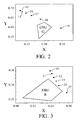
- FIG. 2 shows the shift of the color point of a green-emitting phosphor segment in a plasma screen whose gas contains a mixture of 10% by volume of Xe and 90% by volume of Ne, depending on the proportions of Zn 2 SiO 4 : Mn and Y 0.5 Gd 0.5 ) BO 3 : Tb.
- Color point 14 corresponds to a green-emitting phosphor segment which contains 100% Zn 2 SiO 4 : Mn
- color point 19 corresponds to a phosphor segment which contains 100% (Y 0.5 Gd 0.5 ) BO 3 : Tb.
- the color dots 15 to 18 are the color dots of green-emitting phosphor segments containing a heterogeneous mixture of Zn 2 SiO 4 : Mn and (Y 0.5 Gd 0.5 ) BO 3 : Tb.
- the assignment of the color dots to the respective proportion of the phosphors in the green-emitting phosphor segment is shown in Table 4.
- EBU G denotes the EBU standard for green. ⁇ b> Table 4 ⁇ / b>: Assignment of color points 15 to 18 Color point no.
- FIG. 3 shows the shift of the color point of a red-emitting phosphor segment in a plasma screen whose gas contains a mixture of 10% by volume of Xe and 90% by volume of Ne, depending on the proportions of (Y, Gd) BO 3 : Eu and Y (V, P) O 4 : Eu.
- Color point 20 corresponds to a red-emitting phosphor segment which contains 100% (Y, Gd) BO 3 : Eu and color point 25 corresponds to a red-emitting phosphor segment which contains 100% Y (V, P) O 4 : Eu.
- the color dots 21 to 24 are the color dots of red-emitting phosphor segments containing a heterogeneous mixture of (Y, Gd) BO 3 : Eu and Y (V, P) O 4 : Eu.
- the assignment of the color dots to the respective proportion of the phosphors in the red-emitting phosphor segment is shown in Table 5.
- EBU R is the EBU standard for red. ⁇ b> Table 5 ⁇ / b>: Assignment of color points 21 to 24 Color point no.
- the production process for a phosphor layer 9 which is subdivided into several color segments includes both dry coating methods, for example electrostatic deposition or electrostatically assisted dusting, and wet coating methods, for example screen printing, dispenser methods, in which a suspension with one moving along the channel Nozzle is introduced, or sedimentation from the liquid phase, into consideration.
- the two phosphors of a color segment must be dispersed in water, an organic solvent, optionally together with a dispersing agent, a surfactant and an antifoaming agent or a binder preparation.
- Suitable binders for plasma displays are inorganic binders which survive an operating temperature of 250 ° C without decomposition, embrittlement or discoloration, or organic binders which can later be removed by oxidation.
- the support plate 2 After applying the phosphor layer 9 on a support plate 2, which has address electrodes 10 and a rib structure 12 with barrier ribs, the support plate 2 is used with other components such as a front plate 1 and a noble gas mixture for the production of a plasma display screen.
- the noble gas mixture may contain xenon in a proportion of between 5 and 30% by volume, preferably of 10% by volume.
- one or more color segments may contain a heterogeneous mixture of at least two phosphors emitting the same color. It is particularly preferred that in a plasma display screen having red, green and blue emitting color segments in the phosphor layer 9, each color segment contains a heterogeneous mixture of at least two phosphors emitting the same color.
- a monochrome plasma display panel can also be produced.
- the phosphor layer 9 contains only a heterogeneous mixture of at least two phosphors which emit the same color.
- a screen printing paste containing 30% by weight of (Y, Gd) BO 3 : Tb, 20% by weight of Zn 2 SiO 4 : Mn and 50% of an organic binder was prepared first.
- the paste was applied to a support plate 2 made of glass segmented with a rib structure 12 and address electrodes made of Ag and dried. This process step is carried out one after the other for the other two phosphor types of the emission colors red and blue.
- the screen printing paste for the red color segments contained 50 wt% (Y, Gd) BO 3 : Eu and 50% of an organic binder.
- the screen printing paste for the blue color segment contained 50 wt.% BaMgAl 10 O 17 : Eu and 50% of an organic binder.
- This support plate 2 was used together with a glass faceplate having a dielectric layer 4 of PbO-containing glass, a protective layer 5 of MgO and discharge electrodes 6,7 of ITO to construct an AC plasma display panel.
- the gas filling used was a mixture of 10% by volume of Xe and 90% by volume of Ne.
- the plasma picture screen had greater efficiency and improved luminance.
- a screen printing paste containing 30% by weight of: (Y, Gd) BO 3 : Eu, 20% by weight of Y (V, P) O 4 : Eu and 50% of an organic binder was prepared first.
- the paste was applied to a support plate 2 made of glass segmented with a rib structure 12 and address electrodes made of Ag and dried. This process step is successively for the other two phosphor types the emission colors green and blue performed.
- the screen printing paste for the green color segment contained 50% by weight of Zn 2 SiO 4 : Mn and 50% of an organic binder.
- the screen printing paste for the blue color segment contained 50 wt.% BaMgAl 10 O 17 : Eu and 50% of an organic binder.
- This carrier plate 2 was used together with other components as described in Example 1, for the construction of a plasma picture screen.
- a screen printing paste containing 30% by weight of BaMgAl 10 O 17 : Eu, 20% by weight of YBO 3 : Ce and 50% of an organic binder was first prepared.
- the paste was applied to a support plate 2 made of glass segmented with a rib structure 12 and address electrodes made of Ag and dried. This process step is carried out one after the other for the other two phosphor types of the emission colors red and green.
- the screen printing paste for the green color segment contained 50% by weight of Zn 2 SiO 4 : Mn and 50% of an organic binder.
- the screen printing paste for the red color segment contained 50 wt% (Y, Gd) BO 3 : Eu and 50% of an organic binder.
- This carrier plate 2 was used together with other components as described in Example 1, for the construction of a plasma picture screen.
- a screen printing paste containing 30% by weight of (Y, Gd) BO 3 : Tb, 20% by weight of Zn 2 SiO 4 : Mn and 50% of an organic binder was prepared first.
- the paste was applied to a support plate 2 made of glass segmented with a rib structure 12 and address electrodes made of Ag and dried. This process step is carried out one after the other for the other two phosphor types of the emission colors red and blue.
- the screen printing paste for the red color segment contained 30 wt%: (Y, Gd) BO 3 : Eu, 20 wt% Y (V, P) O 4 : Eu, and 50% of an organic binder.
- the screen printing paste for the blue color segment contained 30 wt%: BaMgAl 10 O 17 : Eu, 20 wt% YBO 3 : Ce and 50% of an organic binder.
- This carrier plate 2 was used together with other components as described in Example 1, for the construction of an improved plasma display screen.
Landscapes
- Chemical & Material Sciences (AREA)
- Engineering & Computer Science (AREA)
- Inorganic Chemistry (AREA)
- Materials Engineering (AREA)
- Organic Chemistry (AREA)
- Physics & Mathematics (AREA)
- Plasma & Fusion (AREA)
- Luminescent Compositions (AREA)
- Gas-Filled Discharge Tubes (AREA)
Applications Claiming Priority (2)
| Application Number | Priority Date | Filing Date | Title |
|---|---|---|---|
| DE10061720 | 2000-12-12 | ||
| DE10061720A DE10061720A1 (de) | 2000-12-12 | 2000-12-12 | Plasmabildschirm mit Leuchtstoffschicht |
Publications (3)
| Publication Number | Publication Date |
|---|---|
| EP1215698A2 EP1215698A2 (de) | 2002-06-19 |
| EP1215698A3 EP1215698A3 (de) | 2005-02-09 |
| EP1215698B1 true EP1215698B1 (de) | 2007-08-08 |
Family
ID=7666731
Family Applications (1)
| Application Number | Title | Priority Date | Filing Date |
|---|---|---|---|
| EP01000719A Expired - Lifetime EP1215698B1 (de) | 2000-12-12 | 2001-12-06 | Plasmabildschirm mit Leuchtstoffschicht |
Country Status (7)
| Country | Link |
|---|---|
| US (1) | US6794821B2 (enExample) |
| EP (1) | EP1215698B1 (enExample) |
| JP (2) | JP4197098B2 (enExample) |
| KR (1) | KR100898199B1 (enExample) |
| CN (1) | CN100557752C (enExample) |
| DE (2) | DE10061720A1 (enExample) |
| TW (1) | TW528997B (enExample) |
Families Citing this family (18)
| Publication number | Priority date | Publication date | Assignee | Title |
|---|---|---|---|---|
| TWI224806B (en) * | 2000-05-12 | 2004-12-01 | Semiconductor Energy Lab | Semiconductor device and manufacturing method thereof |
| TWI290329B (en) * | 2001-10-30 | 2007-11-21 | Hitachi Ltd | Plasma display device, luminescent device and image and information display system using the same |
| KR100490540B1 (ko) * | 2002-11-06 | 2005-05-17 | 삼성에스디아이 주식회사 | 플라즈마 디스플레이 패널 |
| KR100533723B1 (ko) * | 2003-04-25 | 2005-12-06 | 엘지전자 주식회사 | 플라즈마 디스플레이 패널 및 그 제조방법 |
| KR100651277B1 (ko) | 2003-07-25 | 2006-11-28 | 엘지전자 주식회사 | 녹색형광체 및 플라즈마 디스플레이 패널 |
| JP2005116363A (ja) * | 2003-10-08 | 2005-04-28 | Pioneer Plasma Display Corp | プラズマディスプレイパネル |
| KR100669408B1 (ko) * | 2003-11-24 | 2007-01-15 | 삼성에스디아이 주식회사 | 플라즈마 디스플레이 패널 |
| KR100627355B1 (ko) * | 2003-11-28 | 2006-09-21 | 삼성에스디아이 주식회사 | 플라즈마 디스플레이 패널 |
| JP4541832B2 (ja) * | 2004-03-19 | 2010-09-08 | パナソニック株式会社 | プラズマディスプレイパネル |
| KR100918417B1 (ko) * | 2004-05-28 | 2009-09-24 | 삼성에스디아이 주식회사 | 플라즈마 디스플레이 패널 |
| KR20060082527A (ko) * | 2005-01-12 | 2006-07-19 | 삼성에스디아이 주식회사 | 형광체 및 이를 이용한 플라즈마 디스플레이 패널 |
| JP2007007648A (ja) * | 2005-06-30 | 2007-01-18 | Samsung Electronics Co Ltd | 分散剤、それを含むペースト組成物、及びそれを使用して製造される無機素子、並びにそれを含むディスプレイ装置 |
| KR101178053B1 (ko) * | 2005-09-27 | 2012-08-30 | 삼성전자주식회사 | 카르복실 에스테르계 분산제 및 그를 포함하는 황화물계 형광체 페이스트 조성물 |
| KR100904809B1 (ko) * | 2006-02-23 | 2009-06-25 | 파나소닉 주식회사 | 플라즈마디스플레이장치용 녹색형광체 재료의 제조방법 |
| US7705537B2 (en) * | 2006-02-23 | 2010-04-27 | Panasonic Corporation | Plasma display device |
| WO2010016140A1 (ja) * | 2008-08-08 | 2010-02-11 | 株式会社 日立製作所 | 平面表示パネルの制御方法及びプラズマディスプレイパネルの制御方法 |
| DE102008050768C5 (de) † | 2008-10-09 | 2017-11-02 | Bundesdruckerei Gmbh | Sicherheitsmerkmal auf Basis Lumineszenz emittierender Stoffe, Wert- und Sicherheitsdokument mit einem solchen Sicherheitsmerkmal, ein Verfahren sowie eine Vorrichtung zur Verifikation eines solchen Sicherheitsmerkmals |
| JP2010097861A (ja) * | 2008-10-17 | 2010-04-30 | Hitachi Ltd | 表示装置およびプラズマディスプレイパネル |
Family Cites Families (15)
| Publication number | Priority date | Publication date | Assignee | Title |
|---|---|---|---|---|
| KR0133524B1 (ko) * | 1988-12-28 | 1998-04-20 | 아라이 기꾸지 | 형광체 |
| JPH04161483A (ja) * | 1990-10-25 | 1992-06-04 | Kasei Optonix Co Ltd | 発光組成物及び陰極線管用蛍光面 |
| MY109224A (en) * | 1993-02-11 | 1996-12-31 | Samsung Display Devices Co Ltd | Mixed blue emitting phosphor. |
| JPH09219154A (ja) * | 1996-02-08 | 1997-08-19 | Japan Synthetic Rubber Co Ltd | 螢光体組成物およびプラズマディスプレイパネル |
| KR100232136B1 (ko) * | 1996-08-20 | 1999-12-01 | 구자홍 | 칼라 플라즈마 디스플레이 패널의 격벽구조 및 격벽제조방법 |
| JPH10149776A (ja) * | 1996-11-18 | 1998-06-02 | Kasei Optonix Co Ltd | プラズマディスプレイ用蛍光膜 |
| US6013309A (en) * | 1997-02-13 | 2000-01-11 | Lg Electronics Inc. | Protection layer of plasma display panel and method of forming the same |
| JPH10255671A (ja) * | 1997-03-11 | 1998-09-25 | Toray Ind Inc | 蛍光体ペースト |
| DE19727607C2 (de) | 1997-06-28 | 2000-11-23 | Philips Corp Intellectual Pty | Plasmabildschirm mit einer UV-Leuchtstoffzubereitung und UV-Leuchtstoffzubereitung |
| JP4151104B2 (ja) * | 1998-03-31 | 2008-09-17 | 株式会社日立製作所 | プラズマディスプレイ |
| KR20070088816A (ko) * | 1998-10-20 | 2007-08-29 | 코닌클리케 필립스 일렉트로닉스 엔.브이. | 플라즈마 디스플레이 패널 |
| JP2000251701A (ja) * | 1999-02-26 | 2000-09-14 | Toray Ind Inc | ディスプレイの製造方法 |
| US6210605B1 (en) * | 1999-07-26 | 2001-04-03 | General Electric Company | Mn2+ activated green emitting SrAL12O19 luminiscent material |
| JP3797084B2 (ja) * | 1999-12-14 | 2006-07-12 | 松下電器産業株式会社 | プラズマディスプレイ装置 |
| DE10043530A1 (de) * | 2000-09-05 | 2002-03-14 | Philips Corp Intellectual Pty | Farbbildschirm mit blauer Leuchtstoffschicht |
-
2000
- 2000-12-12 DE DE10061720A patent/DE10061720A1/de not_active Withdrawn
-
2001
- 2001-12-06 US US10/011,893 patent/US6794821B2/en not_active Expired - Fee Related
- 2001-12-06 EP EP01000719A patent/EP1215698B1/de not_active Expired - Lifetime
- 2001-12-06 DE DE50112824T patent/DE50112824D1/de not_active Expired - Lifetime
- 2001-12-07 TW TW090130384A patent/TW528997B/zh not_active IP Right Cessation
- 2001-12-07 CN CNB011454911A patent/CN100557752C/zh not_active Expired - Fee Related
- 2001-12-10 KR KR1020010077904A patent/KR100898199B1/ko not_active Expired - Fee Related
- 2001-12-12 JP JP2001378214A patent/JP4197098B2/ja not_active Expired - Fee Related
-
2008
- 2008-04-03 JP JP2008096998A patent/JP4904307B2/ja not_active Expired - Fee Related
Non-Patent Citations (1)
| Title |
|---|
| None * |
Also Published As
| Publication number | Publication date |
|---|---|
| KR100898199B1 (ko) | 2009-05-18 |
| JP4904307B2 (ja) | 2012-03-28 |
| CN1360328A (zh) | 2002-07-24 |
| EP1215698A3 (de) | 2005-02-09 |
| US6794821B2 (en) | 2004-09-21 |
| JP2002251962A (ja) | 2002-09-06 |
| TW528997B (en) | 2003-04-21 |
| JP4197098B2 (ja) | 2008-12-17 |
| EP1215698A2 (de) | 2002-06-19 |
| DE50112824D1 (de) | 2007-09-20 |
| JP2008177174A (ja) | 2008-07-31 |
| KR20020046212A (ko) | 2002-06-20 |
| DE10061720A1 (de) | 2002-06-13 |
| US20020113552A1 (en) | 2002-08-22 |
| CN100557752C (zh) | 2009-11-04 |
Similar Documents
| Publication | Publication Date | Title |
|---|---|---|
| EP1215698B1 (de) | Plasmabildschirm mit Leuchtstoffschicht | |
| DE69824053T2 (de) | Lumineszenzmittel, pulverförmiges Lumineszenzmittel, Plasma-Anzeigetafel, und Herstellungsverfahren derselben | |
| DE19534075C2 (de) | Phosphor | |
| EP1156507B1 (de) | Plasmabildschirm mit einem Terbium(III)-aktivierten Leuchtstoff | |
| DE60300743T2 (de) | Grüner Leuchtstoff und seine Verwendung in Vorrichtungen | |
| DE10009915A1 (de) | Plasmabildschirm mit UV-Licht emittierender Schicht | |
| EP1256616B1 (de) | Plasmabildschirm mit blauem Leuchtstoff | |
| EP1158559A2 (de) | Plasmabildschirm mit Terbium(III)-aktiviertem Leuchtstoff | |
| DE19962029A1 (de) | Plasmabildschirm mit rotem Leuchtstoff | |
| EP1130621A2 (de) | Plasmabildschirm mit blauem Leuchtstoff | |
| EP1187167B1 (de) | Farbbildschirm mit blauer Leuchtstoffschicht | |
| EP1449236B1 (de) | Dielektrische barriere-entladungslampe mit verbesserter farbwiedergabe | |
| EP0999255A2 (de) | Plasmabildschirm mit oxidhaltiger Leuchtstoffzubereitung | |
| DE60313312T2 (de) | Plasmaanzeigetafel enthaltend eine terbium(iii)-aktivierte fluoreszierende substanz | |
| DE10146798A1 (de) | Plasmabildschirm mit erhöhter Effizienz | |
| EP1103591A1 (de) | Plasmabildschirm mit rotem Leuchtstoff | |
| DE60204724T2 (de) | Plasmabildschirm mit grünem phosphor | |
| DE60316087T2 (de) | Plasma-Anzeigetafel mit grünem Leuchtstoff aus Aluminatmischung mit Spinelstruktur | |
| EP1258902A2 (de) | Plasmabildschirm mit verbessertem Weissfarbpunkt | |
| EP1229099A2 (de) | Plasmabildschirm mit einer Leuchtstoffschicht | |
| DE10254175A1 (de) | Plasmabildschirm mit blauemittierendem Leuchtstoff | |
| DE10215891A1 (de) | Plasmabildschirm mit erhöhter Effizienz | |
| DE10210043A1 (de) | Plasmabildschirm mit Pr(III)-aktiviertem Leuchtstoff |
Legal Events
| Date | Code | Title | Description |
|---|---|---|---|
| PUAI | Public reference made under article 153(3) epc to a published international application that has entered the european phase |
Free format text: ORIGINAL CODE: 0009012 |
|
| AK | Designated contracting states |
Kind code of ref document: A2 Designated state(s): AT BE CH CY DE DK ES FI FR GB GR IE IT LI LU MC NL PT SE TR |
|
| AX | Request for extension of the european patent |
Free format text: AL;LT;LV;MK;RO;SI |
|
| RAP1 | Party data changed (applicant data changed or rights of an application transferred) |
Owner name: PHILIPS CORPORATE INTELLECTUAL PROPERTY GMBH Owner name: KONINKLIJKE PHILIPS ELECTRONICS N.V. |
|
| RAP1 | Party data changed (applicant data changed or rights of an application transferred) |
Owner name: PHILIPS INTELLECTUAL PROPERTY & STANDARDS GMBH Owner name: KONINKLIJKE PHILIPS ELECTRONICS N.V. |
|
| PUAL | Search report despatched |
Free format text: ORIGINAL CODE: 0009013 |
|
| AK | Designated contracting states |
Kind code of ref document: A3 Designated state(s): AT BE CH CY DE DK ES FI FR GB GR IE IT LI LU MC NL PT SE TR |
|
| AX | Request for extension of the european patent |
Extension state: AL LT LV MK RO SI |
|
| RIC1 | Information provided on ipc code assigned before grant |
Ipc: 7H 01J 17/49 B Ipc: 7C 09K 11/20 B Ipc: 7H 01J 17/16 B Ipc: 7H 01J 1/63 A |
|
| 17P | Request for examination filed |
Effective date: 20050809 |
|
| AKX | Designation fees paid |
Designated state(s): DE FR GB |
|
| GRAP | Despatch of communication of intention to grant a patent |
Free format text: ORIGINAL CODE: EPIDOSNIGR1 |
|
| RIC1 | Information provided on ipc code assigned before grant |
Ipc: H01J 17/49 20060101ALI20070130BHEP Ipc: H01J 17/16 20060101AFI20070130BHEP |
|
| GRAS | Grant fee paid |
Free format text: ORIGINAL CODE: EPIDOSNIGR3 |
|
| GRAA | (expected) grant |
Free format text: ORIGINAL CODE: 0009210 |
|
| AK | Designated contracting states |
Kind code of ref document: B1 Designated state(s): DE FR GB |
|
| REG | Reference to a national code |
Ref country code: GB Ref legal event code: FG4D Free format text: NOT ENGLISH |
|
| REF | Corresponds to: |
Ref document number: 50112824 Country of ref document: DE Date of ref document: 20070920 Kind code of ref document: P |
|
| GBT | Gb: translation of ep patent filed (gb section 77(6)(a)/1977) |
Effective date: 20070912 |
|
| ET | Fr: translation filed | ||
| PLBE | No opposition filed within time limit |
Free format text: ORIGINAL CODE: 0009261 |
|
| STAA | Information on the status of an ep patent application or granted ep patent |
Free format text: STATUS: NO OPPOSITION FILED WITHIN TIME LIMIT |
|
| 26N | No opposition filed |
Effective date: 20080509 |
|
| REG | Reference to a national code |
Ref country code: GB Ref legal event code: 732E Free format text: REGISTERED BETWEEN 20100204 AND 20100211 |
|
| REG | Reference to a national code |
Ref country code: FR Ref legal event code: TP |
|
| REG | Reference to a national code |
Ref country code: FR Ref legal event code: RM |
|
| PGFP | Annual fee paid to national office [announced via postgrant information from national office to epo] |
Ref country code: GB Payment date: 20131112 Year of fee payment: 13 Ref country code: FR Payment date: 20131115 Year of fee payment: 13 Ref country code: DE Payment date: 20131113 Year of fee payment: 13 |
|
| REG | Reference to a national code |
Ref country code: DE Ref legal event code: R119 Ref document number: 50112824 Country of ref document: DE |
|
| GBPC | Gb: european patent ceased through non-payment of renewal fee |
Effective date: 20141206 |
|
| REG | Reference to a national code |
Ref country code: FR Ref legal event code: ST Effective date: 20150831 |
|
| PG25 | Lapsed in a contracting state [announced via postgrant information from national office to epo] |
Ref country code: DE Free format text: LAPSE BECAUSE OF NON-PAYMENT OF DUE FEES Effective date: 20150701 Ref country code: GB Free format text: LAPSE BECAUSE OF NON-PAYMENT OF DUE FEES Effective date: 20141206 |
|
| PG25 | Lapsed in a contracting state [announced via postgrant information from national office to epo] |
Ref country code: FR Free format text: LAPSE BECAUSE OF NON-PAYMENT OF DUE FEES Effective date: 20141231 |