EP1202151A2 - Dispositif de commande de données et équipement électronique - Google Patents
Dispositif de commande de données et équipement électronique Download PDFInfo
- Publication number
- EP1202151A2 EP1202151A2 EP01125404A EP01125404A EP1202151A2 EP 1202151 A2 EP1202151 A2 EP 1202151A2 EP 01125404 A EP01125404 A EP 01125404A EP 01125404 A EP01125404 A EP 01125404A EP 1202151 A2 EP1202151 A2 EP 1202151A2
- Authority
- EP
- European Patent Office
- Prior art keywords
- clock
- data transfer
- control device
- transfer control
- circuit
- Prior art date
- Legal status (The legal status is an assumption and is not a legal conclusion. Google has not performed a legal analysis and makes no representation as to the accuracy of the status listed.)
- Withdrawn
Links
Images


Classifications
-
- H—ELECTRICITY
- H03—ELECTRONIC CIRCUITRY
- H03L—AUTOMATIC CONTROL, STARTING, SYNCHRONISATION OR STABILISATION OF GENERATORS OF ELECTRONIC OSCILLATIONS OR PULSES
- H03L7/00—Automatic control of frequency or phase; Synchronisation
- H03L7/06—Automatic control of frequency or phase; Synchronisation using a reference signal applied to a frequency- or phase-locked loop
- H03L7/07—Automatic control of frequency or phase; Synchronisation using a reference signal applied to a frequency- or phase-locked loop using several loops, e.g. for redundant clock signal generation
-
- G—PHYSICS
- G06—COMPUTING OR CALCULATING; COUNTING
- G06F—ELECTRIC DIGITAL DATA PROCESSING
- G06F13/00—Interconnection of, or transfer of information or other signals between, memories, input/output devices or central processing units
-
- G—PHYSICS
- G06—COMPUTING OR CALCULATING; COUNTING
- G06F—ELECTRIC DIGITAL DATA PROCESSING
- G06F1/00—Details not covered by groups G06F3/00 - G06F13/00 and G06F21/00
- G06F1/04—Generating or distributing clock signals or signals derived directly therefrom
- G06F1/06—Clock generators producing several clock signals
-
- H—ELECTRICITY
- H03—ELECTRONIC CIRCUITRY
- H03L—AUTOMATIC CONTROL, STARTING, SYNCHRONISATION OR STABILISATION OF GENERATORS OF ELECTRONIC OSCILLATIONS OR PULSES
- H03L7/00—Automatic control of frequency or phase; Synchronisation
- H03L7/06—Automatic control of frequency or phase; Synchronisation using a reference signal applied to a frequency- or phase-locked loop
- H03L7/08—Details of the phase-locked loop
- H03L7/099—Details of the phase-locked loop concerning mainly the controlled oscillator of the loop
- H03L7/0995—Details of the phase-locked loop concerning mainly the controlled oscillator of the loop the oscillator comprising a ring oscillator
-
- H—ELECTRICITY
- H03—ELECTRONIC CIRCUITRY
- H03L—AUTOMATIC CONTROL, STARTING, SYNCHRONISATION OR STABILISATION OF GENERATORS OF ELECTRONIC OSCILLATIONS OR PULSES
- H03L7/00—Automatic control of frequency or phase; Synchronisation
- H03L7/06—Automatic control of frequency or phase; Synchronisation using a reference signal applied to a frequency- or phase-locked loop
- H03L7/16—Indirect frequency synthesis, i.e. generating a desired one of a number of predetermined frequencies using a frequency- or phase-locked loop
- H03L7/18—Indirect frequency synthesis, i.e. generating a desired one of a number of predetermined frequencies using a frequency- or phase-locked loop using a frequency divider or counter in the loop
Definitions
- the present invention relates to a data transfer control device and electronic equipment.
- USB universal serial bus
- this USB standard In comparison with the IEEE 1394 standard which is also attracting notice as a standard for the same serial bus interface, this USB standard has a problem in that the transfer speed thereof is slower.
- USB 2.0 transceiver macrocell interface which defines interface specifications for the physical-layer and logical-layer circuitry under USB 2.0, has also been decided upon.
- USB 2.0 In addition to the full-speed (FS) mode defined by the prior-art USB 1.1, USB 2.0 provided a transfer mode called high-speed (HS) mode. Since data transfer in this HS mode is at 480 Mbps, it is possible to implement data transfer at a much higher speed than the data transfer at 12 Mbps of FS mode. This USB 2.0 therefore makes it possible to provide an interface that is optimal for storage devices such as hard disk drives and optical disk drives that require fast transfer speeds.
- HS high-speed
- the present invention is devised in the light of the above-described technical problems, making it possible to provide a data transfer control device and electronic equipment that are capable of switching the frequency of the generated clock in a dynamic manner but without causing operational errors .
- the present invention can provide a data transfer control device and electronic equipment that make it possible to implement data transfer in different transfer modes, with a reduced power consumption.
- one aspect of the present invention relates to a data transfer control device for transferring data over a bus, the data transfer control device comprising:
- the present invention generates the system clock used within the data transfer control device or by later-stage data processing circuits based on first and second clocks generated by the clock generation circuit.
- the present invention also enables the operation of generating the second clock by the clock generation circuit before disabling the operation of generating the first clock.
- the source clock for the generation of the system clock is switched from the first clock to the second clock, so that the system clock generation is based on the second clock instead of the first clock.
- the operation of generating the first clock is disabled after the clock switchover, the power that would be consumed by the operation of generating the first clock can be saved, thus reducing the power consumption of the data transfer control device.
- the clock generation circuit may comprise a first PLL (phase locked loop) which generates a first clock and a second PLL which generates a second clock
- the clock control circuit may enable autonomous operation of the second PLL before disabling autonomous operation of the first PLL, and may switch the clock used for generating the system clock from the first clock to the second clock after confirming that the autonomous operation of the second PLL has stabilized.
- the clock control circuit may set the system clock to a first level during a given period when the clock used for generating the system clock switches over from the first clock to the second clock.
- processing for setting the system clock to the first level could be implemented by an AND operation of the first or second clock and a mask signal that is at the first level during a given clock-switching period.
- a setting of the given period, during which the system clock is set to a first level may be based on a base clock used for the clock generation by the clock generation circuit.
- the clock control circuit may set the system clock, which is generated based on the first clock, to a first level on condition that the first clock has become the first level, and may generate the system clock based on the second clock on condition that the second clock has become the first level.
- This enables efficient prevention of the generation of glitches in the system clock at clock switchover.
- the generation of the system clock is based on the second clock after the second clock has changed from the second level to the first level, but before it changes back from the first level to the second level. It is therefore possible to prevent a situation in which pulses of the system clock become tiny glitches.
- Another aspect of the present invention relates to a data transfer control device for transferring data over a bus, the data transfer control device comprising:
- the present invention ensures that the generation of the system clock used by the interior of the data transfer control device or the later-stage data processing circuitry is based on the first and second clocks generated by the clock generation circuit.
- the present invention also ensures that the system clock is set to the first level at the switchover of the clock used as the generation source of the system clock. It is therefore possible to prevent a situation in which a clock that has been made unstable by the clock switchover is supplied to the interior of the data transfer control device or the later-stage data processing circuitry, and also connect the first and the second clock as suitable even if the phases of the first and second clocks do not match.
- Yet another aspect of the present invention relates to a data transfer control device for transferring data over a bus, the data transfer control device comprising:
- the present invention ensures that the generation of the system clock used by the interior of the data transfer control device or the later-stage data processing circuitry is based on the first and second clocks generated by the clock generation circuit.
- the present invention also ensures that the system clock can be fixed at the first level after the first clock has changed from the second level to the first level at the switchover of the clock that is to be used as the generation source for the system clock. If the second clock changes from the second level to the first level after the system clock has been fixed at the first level in this manner, the generation of the system clock can be based on the second clock.
- This configuration makes it possible to prevent the occurrence of glitches in the system clock, thus making it possible to ensure stable operation of the data transfer control device and data processing circuitry in later stages.
- the present invention makes it possible to perform operations such as data transfer and system clock generation, based on a first clock generated by the first PLL in a high-speed first transfer mode.
- operations such as data transfer and system clock generation, based on a first clock generated by the first PLL in a high-speed first transfer mode.
- the autonomous operation of the first PLL is disabled.
- the first PLL that is not necessary in the second transfer mode can therefore be disabled during operation in the second transfer mode, thus preventing any wasteful consumption of power by the first PLL and enabling reductions in the power consumption of the data transfer control device itself.
- a port connected to a bus supports the first transfer mode, in a state of operation in accordance with the first clock generated by the first PLL, and, when it is detected that the first transfer mode is not supported, autonomous operation of the first PLL may be disabled based on a selection signal from a later-stage data processing circuit.
- the clock control circuit may enable autonomous operation of the second PLL before disabling autonomous operation of the first PLL, and may disable autonomous operation of the first PLL after confirming that autonomous operation of the second PLL has stabilized.
- USB universal serial bus
- the present invention makes it possible to guarantee stable operation of the data transfer control device at switchover from HS mode to FS mode and at switchover from FS mode to HS mode.
- Electronic equipment in accordance with the present invention may comprise any of the above described data transfer control devices, and a device which performs output processing, fetch processing, or storage processing on data transferred through the data transfer control device and the bus.
- the present invention makes it possible to reduce the cost and improve the reliability of a data transfer control device used in electronic equipment, it also makes it possible to reduce the cost and improve the reliability of the electronic equipment itself. Since the present invention also makes it possible to implement data transfer in a high-speed transfer mode, it helps increase the processing speed of the electronic equipment.
- the present invention also makes it possible to use a clock that has been optimized for the transfer mode in use, making it possible to further reduce the power consumption of the electronic equipment.
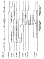
- FIG. 1 An example of the configuration of a data transfer control device in accordance with an embodiment of the present invention is shown in Fig. 1.
- the data transfer control device of this embodiment of the present invention comprises a data handler circuit 400, a high-speed (HS) circuit 410, a full-speed (FS) circuit 420, an analog front-end circuit 430, a clock generation circuit 440, and a clock control circuit 450. Note that not all of the circuit blocks shown in Fig. 1 are necessary for the data transfer control device of the present invention; some of them may be omitted.
- the data handler circuit 400 (generally speaking: a given circuit for performing data transfer) performs various types of processing for transferring data in conformation with a standard such as USB. More specifically, during transmission, it performs processing such as attaching synchronization (SYNC) , start of packet (SOP), and end of packet (EOP) codes to the data to be transmitted, and bit stuffing. During reception, on the other hand, it performs processing to detect and remove the SYNC, SOP, and EOP codes, and bit unstuffing. In addition it generates various timing signals for controlling the data transfer.
- SYNC attaching synchronization
- SOP start of packet
- EOP end of packet
- received data is output to a serial interface engine (SIE) that is a circuit (data processing means) in a stage after the data handler circuit 400, and data to be transmitted is input to the data handler circuit 400 from the SIE.
- SIE serial interface engine
- the HS circuit 410 is a logic circuit for transferring data at high speed (HS), which is a data transfer speed of 480 Mbps
- the FS circuit 420 is a logic circuit for transferring data at a full speed (FS), which is a data transfer speed of 12 Mbps.
- HS mode is a new transfer mode that has been defined by USB 2.0.
- FS mode is a transfer mode that was defined previously by USB 1.1.
- USB 2.0 provides this HS mode, it makes it possible to implement not only data transfer for devices such as printers, audio equipment, and cameras, but also data transfer in storage devices such as hard disk drives or optical disk (CD-ROM or DVD) drives.
- the HS circuit 410 comprises a high-speed delay line PLL (HSDLL) circuit 10 and an elasticity buffer 12.
- HSDLL high-speed delay line
- the HSDLL circuit 10 is a circuit that generates a data sampling clock based on received data and a clock from the clock generation circuit 440 (PLL).
- the elasticity buffer 12 is a circuit for absorbing any difference in clock frequency (clock drift) between the internal device (the data transfer control device) and an external device (an external device connected to the bus).
- the analog front-end circuit 430 is an analog circuit comprising drivers and receivers for transfer at FS and HS. With USB, data is transferred by a differential signal, using data-plus (DP) and data-minus (DM) signals.
- DP data-plus
- DM data-minus
- the clock generation circuit 440 generates a 480-MHz clock used within the device and a 60-MHz clock used within the device and by the SIE.
- the clock generation circuit 440 comprises an oscillation circuit (OSC), a PLL480M, and a PLL60M.
- OSC oscillation circuit
- PLL480M PLL480M
- PLL60M PLL60M
- the OSC generates a base clock in combination with another component such as an external oscillator, by way of example.
- the PLL480M is a phase-locked loop (PLL) that generates the 480-MHz clock necessary for HS mode as well as the 60-MHz clock necessary for FS mode, various components within the device, and the SIE, based on the base clock generated by the OSC. Note that when transfer is in HS mode, it is necessary to validate clock generation by this PLL480M.
- PLL phase-locked loop
- the PLL60M generates the 60-MHz clock necessary for FS mode, various components within the device, and the SIE, based on the base clock generated by the oscillation circuit 20. Note that transfer in HS mode is not possible when clock generation by this PLL60M is enabled.
- the clock control circuit 450 receives various control signals from the SIE and performs processing such as control of the clock generation circuit 440. Note that the 60-MHz system clock generated by the clock generation circuit 440 is output to the SIE through the clock control circuit 450.
- FIG. 2 An example of the configuration of the clock generation circuit 440 (clock generation means) and the clock control circuit 450 (clock control means) in accordance with this embodiment is shown in Fig. 2.
- the oscillation circuit (OSC) comprised within the clock generation circuit 440 uses an external oscillator connected to XIN and XOUT to oscillate, generating a base clock RCLK (of, for example, 12 to 24 MHz). This base clock RCLK is output to the PLL480M, the PLL60M, and the clock control circuit 450.
- OSC oscillation circuit
- OSCENB is a signal for validating/invalidating the oscillation of OSC and the input of the external clock from XI. If OSCENB becomes "0" (logic level, hereinafter the same), by way of example, the OSC oscillation and the input of the external clock are invalidated; if it becomes "1", they are validated. If OSCENB goes to "0" when the device has been put into a suspended state by SUSPENDM, by way of example, it is possible to transit to a completely suspended state in which even OSC does not operate.
- the PLL480M comprised by the clock generation circuit 440 generates a 480-MHz clock that is phase-synchronized with the base clock RCLK, when the condition is satisfied that a ENB480M from the clock control circuit 450 is "1".
- a 60-MHz clock obtained by dividing this 480-MHz clock is output as CLKH to the clock control circuit 450. Note that the division of the 480-MHz clock could also be done on the clock control circuit 450 side.
- the PLL60M comprised by the clock generation circuit 440 generates a 60-MHz clock that is phase-synchronized with the base clock RCLK, when the condition is satisfied that a ENB60M signal from the clock control circuit 450 is "1". This 60-MHz is output to the clock control circuit 450 as CLKF.
- the clock control circuit 450 receives the SUSPENDM and PLLSEL signals from the serial interface engine (SIE) and controls the clock generation operation by the clock generation circuit 440 (autonomous operation of the PLL480M and the PLL60M) . It also generates and outputs a system clock SYCLK (reference clock for synchronization) used within the data transfer control device and by the SIE (later-stage data processing means), based on the clocks CLKH and CLKF generated by the clock generation circuit 440.
- SIE serial interface engine
- SUSPENDM is a signal for suspending the data transfer control device (transceiver macro). If the transfer control device is suspended by making SUSPENDM go to "0", all circuits other than the oscillation circuit (OSC) halt.
- OSC oscillation circuit
- PLLSEL is a signal that enables the SIE to select which of the PLL480M and the PLL60M is to operate autonomously; when PLLSEL is "0" the PLL480M is selected and when it is “1” the PLL60M is selected. Note that it is necessary to make PLLSEL go to "0" select the PLL480M, when transferring a "chirp" in HS mode.
- STABLE480M goes to "1" at a time at which it is assumed that the autonomous operation of the PLL480M has stabilized (at a time at which it is assumed that the 480 MHz ⁇ 500 ppm clock required for the USB 2.0 standard is being generated).
- the configuration is such that a SYCLKENB signal (SYCLK mask signal) goes to "1" and the system clock SYCLK (a 60-MHz clock) generated by CLKH (the 60-MHz clock divided from 480 MHz) from the PLL480M is supplied to the interior of the data transfer control device and the SIE (later-stage data processing means).
- SYCLKENB signal SYCLK mask signal
- SYCLK system clock generated by CLKH (the 60-MHz clock divided from 480 MHz) from the PLL480M is supplied to the interior of the data transfer control device and the SIE (later-stage data processing means).
- a count based on the base clock RCLK from the oscillation circuit OSC is performed in order to measure the period between T1 and T3 in Fig. 3 (the period required for the autonomous operation of the PLL480M to stabilize).
- This RCLK becomes a stable clock after the OSCENB of Fig. 2 has gone to "1" and the oscillation of the oscillation circuit OSC has stabilized. Use of this RCLK therefore makes it possible to measure the period from T1 to T3 stably.
- a count based on the base clock RCLK starts, and STABLE60M (a signal indicating that the autonomous operation of the PLL60M has stabilized) goes to "1" when that count ends at a time T6, causing a switch in clocks by using SYCLKENB, which is the system clock SYCLK mask signal.
- SYCLKENB which is the system clock SYCLK mask signal.
- the system clock SYCLK supplied to the interior of the data transfer control device and the SIE is based on CLKH from the PLL480M before the clocks are switched, whereas it is based on CLKF from the PLL60M after the switch.
- the autonomous operation of the PLL60M is enabled (started), as shown at A2 in Fig. 3, before the autonomous operation (clock generation operation) of the PLL480M is disabled (ended), as shown at A1.
- the clock used for the generation of the system clock SYCLK is switched from CLKH (the PLL480M) to CLKF (the PLL60M), as shown at A4, after it is determined that the autonomous operation of the PLL60M has stabilized, as shown at A3.
- the PLL480M can be disabled and the PLL60M can subsequently operate alone. It is therefore possible to reduce the power consumption of the PLL480M to close to zero, making is possible to greatly reduce the power consumption of the entire data transfer control device.
- the configuration is such that the PLL480M operates in the faster HS mode so that SYCLK is generated from CLKH from the PLL480M, whereas the operation of the PLL480M is halted in the slower FS mode and SYCLK is generated from CLKF from the PLL60M.
- the PLL480M operates in FS mode, preventing wasteful power consumption in FS mode and thus enabling a large reduction in power consumption in FS mode.
- a configuration could be considered in which only the PLL480M is provided as a clock generation circuit and the system clock SYCLK in FS mode is generated by dividing the clock from the PLL480M, as a comparative example.
- the PLL480M operates even in FS mode, wasting power in FS mode and thus making it impossible to reduce the power consumption in FS mode.
- this embodiment of the invention is configured so that the PLL480M does not operate in FS mode, leaving the less power-intensive PLL60M to operate alone, making it possible to greatly reduce the power consumption in FS mode in comparison with the above-described comparative example.
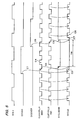
- Timing waveform charts shown in Figs. 4 and 5 illustrate the operation of this embodiment of the invention during the clock switchover (times T4 to T7 in Fig. 3).
- a DCOVER signal goes to "1" at the next rising edge of RCLK, as shown at B3 in Fig. 4. This changes the STABLE60M signal from “0" to "1", as shown at B4.
- the SYCLKENB signal is generated to go to "0" (a first level) in a clock switchover period, as shown at B5 in Fig. 4, by performing a logical OR on these STABLE480M and STABLE60M signals, by way of example.
- the configuration is such that SYCLK is held at "0" (a first level, which could also be “1"), as shown at B6, by using the SYCLKENB signal to mask the system clock SYCLK (by ANDing SYCLKENB and SYCLK).
- the system clock SYCLK is set to "0" during a period TM in which the clock used for generating SYCLK is being switched from CLKH (the PLL480M) to CLKF (the PLL60M).
- CLKH the PLL480M
- CLKF the PLL60M
- This therefore ensures that a clock that has been made unstable by the switchover from CLKH to CLKF is not supplied as SYCLK to the data transfer control device and SIE (later-stage data processing means).
- SIE later-stage data processing means
- the setting of the period TM during with the system clock SYCLK is set to "0" is based on the base clock RCLK (of, for example, 12 to 24 MHz) used in clock generation by the PLL480M and the PLL60M.
- the period TM is the space between the edges of RCLK (the length of one clock pulse of RCLK) shown at B1 and B3 in Fig. 4. It is therefore possible to base the setting of the length of the clock switchover period TM on the base clock RCLK that is in a stable signal state even during the switchover.
- CLKH and CLKF can be masked reliably by using the signal SYCLKENB.
- the system detects CLKH from the PLL480M reaches "0" (waits until it reaches "0"), as shown at C1 in Fig. 5.
- the mask signal SYCLKENB is set to "0" when the condition is satisfied that CLKH has reached "0" (a first level, or at the falling edge of CLKH) and the system clock SYCLK, which is generated from an AND of SYCLKENB and CLKH, is fixed at the "0" level, as shown at C2 in Fig. 5.
- the count operation of the base clock RCLK then starts (state S3), then the system detects the clock CLKH from the PLL480M becoming “0" (state S4).
- the clock CLKH is output as the system clock SYCLK when the condition is satisfied that CLKH has become “0" (state S5), and the system changes to the normal operating state S6. If CLKH is output as SYCLK only on condition that CLKH has become “0” in this manner, it is possible to efficiently prevent the generation of glitches in SYCLK.
- the ENB60M signal goes to "1" (state S7), enabling the autonomous operation of the PLL60M.
- the count operation of the base clock RCLK then starts (state S8) and the system detects the clock CLKF from the PLL60M becoming "0" after the count ends (state S9).
- the CLKF clock is output as SYCLK when the condition is satisfied that CLKF has become “0” (state S10), and the system changes to the normal operating state S6.
- the ENB60M signal is set to “1" (state S20 in Fig. 7).
- the count operation of the base clock RCLK starts (state S21)
- the system detects the clock CLKH from the PLL480M becoming “0” after the count ends (state S22, or C1 in Fig. 5).
- CLKH becomes "0”
- the output of SYCLK is halted by using the mask signal SYCLKENB (state S23, or C2 in Fig. 5).
- the system then detects the clock CLKF from the PLL60M becoming “0" (state S24, or C5 in Fig. 5).
- CLKF becomes "0"
- the SYCLKENB signal is set to "1" (C6 in Fig. 5)
- CLKF is output as the system clock SYCLK (state S25), and the system transitions to the normal operating state S6, as shown in Fig. 6.
- the clock switchover illustrated by states S22 to S25 in Fig. 7 makes it possible to efficiently prevent the generation of glitches in the system clock SYCLK during the switchover from CLKH to CLKF.
- the clock switchover illustrated by states S32 to S35 in Fig. 8 makes it possible to efficiently prevent the generation of glitches in the system clock SYCLK during the switchover from CLKF to CLKH.
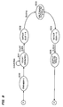
- FIG. 9 A detailed example of the configuration of the PLL480M is shown in Fig. 9.
- This PLL480M comprises a phase comparator 80, a charge pump circuit 82, a filter circuit 84, a voltage-controlled oscillator (VCO) 86, and a clock divider 88.
- VCO voltage-controlled oscillator
- the phase comparator 80 compares the phases of the base clock RCLK (of, for example, 12 to 24 MHz) and a clock DCLK4 from the clock divider 88, then outputs a phase error signal PUP or PDW (where PUP is a phase-advanced signal and PDW is a phase-retarded signal).
- the charge pump circuit 82 operates as a charge pump on the basis of the PUP or PDW signal from the phase comparator 80. More specifically, if PUP is active, the charge pump circuit 82 charges a capacitor within the filter circuit 84; if PDW is active, it discharges the capacitor. A control voltage VC that has been smoothed by the filter circuit 84 is given to the VCO 86.
- the VCO 86 performs an oscillation operation wherein the oscillation frequency is controlled in a variable manner in accordance with the control voltage VC, to generate 480-MHz clocks QCLK0 to QCLK4. If the control voltage VC is high, by way of example, the oscillation frequency also increases; if the control voltage VC is low, the oscillation frequency also decreases.
- the clocks QCLK0 to QCLK4 generated by the VCO 86 are output to the exterior as CLK0 to CLK4 through buffers BF00 to BF04 and BF10 to BF14.
- BF20 to BF23 denote dummy buffer circuits for load-combining with another buffer circuit BF24.
- the clock divider 88 takes the clock QCLK4 that is input from the VCO 86 through the buffer circuits BF04 and BF24, divides it (1/N), and outputs the result of the division as the clock DCLK4 to the phase comparator 80.
- FIG. 10 An example of the configuration of the VCO 86 of Fig. 9 is shown in Fig. 10.
- This VCO 86 comprises five stages (generally speaking: an odd number of stages) of serially-connected differential output comparators DCP0 to DCP4 (inversion circuits), such that differential outputs Q and XQ of each of DCP0 to DCP4 are input to differential inputs of single-end output comparators SCP0 to SCP4. Outputs of SCP0 to SCP4 become the output clocks QCLK0 to QCLK4 of the VCO 86. If the control voltage VC changes, the current flowing through the current source of the differential output comparators DCP0 to DCP4 also changes, so the oscillation frequency changes.
- FIG. 11 A detailed example of the configuration of the PLL60M is shown in Fig. 11.
- This PLL60M comprises a clock divider 89, a phase comparator 90, a charge pump circuit 92, a filter circuit 94, a VCO 96, and clock dividers 97 and 98.
- the phase comparator 90 compares the phases of a clock DRCLK from the clock divider 89 (a clock which is divided from the base clock RCLK) and a clock DCLKF from the clock divider 98, and outputs the phase error signal PUP or PDW.
- the charge pump circuit 92 operates as a charge pump on the basis of the PUP or PDW signal from the phase comparator 90. More specifically, if PUP is active, the charge pump circuit 92 charges a capacitor within the filter circuit 94; if PDW is active, it discharges the capacitor. A control voltage VC that has been smoothed by the filter circuit 94 is given to the VCO 96.
- the VCO 96 performs an oscillation operation wherein the oscillation frequency is controlled in a variable manner in accordance with the control voltage VC, to generate a 120-MHz clock QCLK.
- the clock divider 97 divides the clock QCLK that is input from the VCO 96 (1/2) and outputs the thus-divided 60-MHz clock CLKF to the clock control circuit 450 of Fig. 2.
- the clock divider 98 divides a clock QCLKF that is input from the clock divider 97 (1/N) and outputs the thus-divided clock DCLKF to the phase comparator 90.
- FIG. 12 An example of the configuration of the VCO 96 of Fig. 11 is shown in Fig. 12.
- This VCO 96 comprises three stages of serially connected differential output comparators DCP10 to DCP12 (inversion circuits). Differential outputs XQ and Q of the final-stage differential output comparator DCP12 are input to differential inputs of a single-end output comparator SCP10, and the output of SCP10 becomes the output clock QCLK of the VCO 96. If the control voltage VC changes, the current flowing through the current source of the differential output comparators DCP10 to DCP12 also changes, changing the oscillation frequency.
- differential output comparator (differential amplifier) comprised within the VCO of Figs. 10 and 12 is shown in Fig. 13A.
- This differential output comparator comprises transistors NT1 and NT2, where differential inputs I and XI are connected to the gate electrodes thereof and differential outputs XQ and Q are connected to the drain electrodes thereof; p-type transistors PT1 and PT2, where the differential output Q is connected to both gate electrodes thereof and the differential outputs XQ and Q are connected to the drain electrodes thereof; and an n-type transistor NT3 (current source), where the control voltage VC is connected to the gate electrode thereof.
- the VCO 96 (120-MHz oscillation) of Fig. 12 can be optimized for use with 120 MHz (or 60 MHz) oscillation by selecting factors such as the sizes of the transistors comprised within the differential output comparators DCP10 to DCP12 and the single-end output comparator SCP10. It is therefore possible to greatly reduce the power consumption of the VCO 96 of Fig. 12 in comparison with that of the VCO 86 (480-MHz oscillation) of Fig. 10. For that reason, the current consumption of the PLL60M comprised within the VCO 96 of Fig. 12 becomes extremely small, approximately 1.5 mA, in contrast to the extremely high current consumption of the PLL480M comprised within the VCO 86 of Fig. 10, which is approximately 33 mA, by way of example.
- the clock is generated by using the PLL480M, but if the operation of the PLL480M is halted and the PLL60M alone is used to generate the clock in FS mode, it becomes possible to reduce the current consumed by the PLL to approximately 1/22, by way of example, making it possible to reduce the power consumption of the data transfer control device.
- PLL480M and PLL60M of Figs. 9 and 11 could also be configured to not have the charge pump circuits 82 and 92.
- current-controlled oscillation means could be provided instead of the VCOs 86 and 96.
- the inversions circuits comprised within the VCOs 86 and 96 are not limited to differential output comparators and thus various modifications are possible.
- p-type transistors PT4 and PT5 and n-type transistors NT4 and NT5 could be connected in series to form the inversion circuit shown in Fig. 13B.
- the current flowing in these transistors is controlled by control voltages VCQ and VC connected to the gate electrodes of PT4 and NTS, providing variable control of the oscillation frequency.
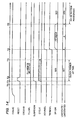
- a timing waveform chart shown in Fig. 14 relates to an example in which the data transfer control device (electronic equipment) of this embodiment of the invention has been connected to a bus (device attachment).
- this data transfer control device starts operating in HS mode. For that reason, the PLLSEL is set to "0" (the PLL480M is selected). Both XCVRSEL (a signal that validates the HS transceiver when at “0” or the FS transceiver when at “1”) and TERMSEL (a signal that validates HS termination when at "0" and FS termination when at “1") are set to "0".
- the SIE asserts a RESET signal and also negates the SUSPENDM signal at a time T1.
- PLLSET is set to "0" and thus the PLL480M is selected, so the autonomous operation of the PLL480M is enabled.
- the RESET signal is negated at time T2 and the stabilized clock CLKH from the PLL480M is output at time T3.
- the system clock SYCLK generated based on this CLKH is supplied to the SIE.
- the XCVRSEL and TERMSEL signals go to "1" at time T4, validating the FS transceiver and FS termination.
- a reset (SE0) is sent from a downstream port at time T5, and HS detection handshake starts.
- a timing waveform chart for HS detection handshake that is shown in Fig. 15 relates to an example in which a port that does not support HS mode is connected to this data transfer control device.
- the HS detection handshake starts at time T0 in Fig. 15.
- the XCVRSEL signal goes to "0" at time T1, validating the HS transceiver.
- the transmission of a chirp (K) starts. Note that bit-stuffing (BS) processing and NRZI processing are disabled during the transmission of this chirp (K) and data stuffed with zeros is output.
- BS bit-stuffing
- NRZI processing are disabled during the transmission of this chirp (K) and data stuffed with zeros is output.
- the transmission of the chirp (K) ends at time T2. If the downstream port supports HS mode, the transmission of the chirp (K) starts at time T3. However, since the chirp cannot be detected at time T4, the data transfer control device of this embodiment of the present invention returns to FS mode at that point and waits for the end of the reset sequence.
- the reset sequence ends at time T6 and a transition to normal operation in FS mode occurs at time T7.
- the transfer mode is defined as FS mode by this time T4. Since there is a reset phase for FS mode between the times T4 and T6, there is no transfer of packets then.
- the SIE sets the PLLSEL signal to "1" at the time T5 between the times T4 and T6, which disables the autonomous operation of the PLL480M and also enables the autonomous operation of the PLL60M.
- a clock switchover occurs as described with reference to Fig. 3, so that the clock used as the generation source of the system clock SYCLK switches from the clock CLKH of the PLL480M to the clock CLKF of the PLL60M.
- this data transfer control device detects whether or not the port connected to the bus supports HS mode (the first transfer mode) in a state in which operation is based on the clock CLKH from the PLL480M.
- the autonomous operation of the PLL480M is disabled by the PLLSEL signal (selection signal) from the SIE (later-stage data processing means). This ensures that subsequent operation by the data transfer control device and the SIE is based on the clock CLKF from the PLL60M. Since the autonomous operation of the PLL480M has been disabled, it is possible to prevent wasteful consumption of power by this PLL480M, enabling a reduction in the power consumption of the data transfer control device.
- FIG. 16A An internal block diagram of a printer that is one example of such electronic equipment is shown in Fig. 16A with an external view thereof being shown in Fig. 17A.
- a CPU (microcomputer) 510 has various functions, including that of controlling the entire system.
- An operating section 511 is designed to enable the user to operate the printer.
- Data such as a control program and fonts is stored in a ROM 516, and a RAM 517 functions as a work area for the CPU 510.
- a DMAC 518 is a DMA controller for transferring data through the CPU 510.
- a display panel 519 is designed to inform the user of the operational state of the printer.
- Serial print data that has been send in from another device such as a personal computer via USB is converted into parallel print data by a data transfer control device 500.
- the thus converted parallel print data is sent to a print processing section (a printer engine) 512 by the CPU 510 or the DMAC 518.
- This parallel print data is subjected to given processing in the print processing section 512 and is output for printing to paper by a printing section (a device for outputting data) 514 comprising components such as a print head.
- FIG. 16B An internal block diagram of a scanner that is another example of electronic equipment is shown in Fig. 16B with an external view thereof being shown in Fig. 17B.
- a CPU 520 has various functions, including that of controlling the entire system.
- An operating section 521 is designed to enable the user to operate the scanner.
- Data such as a control program is stored in a ROM 526, and a RAM 527 functions as a work area for the CPU 520.
- a DMAC 528 is a DMA controller.
- An image of a document is read in by an image read section (a device for fetching data) 522, which comprises components such as a light source and an opto-electric converter, and data of the read-in image is processed by an image processing section (a scanner engine) 524.
- the processed image data is sent to the data transfer control device 500 by the CPU 520 or DMAC 528.
- the data transfer control device 500 converts that parallel image data into serial data and sends it to another device such as a personal computer via USB.
- FIG. 16C An internal block diagram of a CD-RW drive that is a further example of electronic equipment is shown in Fig. 16C with an external view thereof being shown in Fig. 17C.
- a CPU 530 has various functions, including that of controlling the entire system.
- An operating section 531 is designed to enable the user to operate the CD-RW drive.
- Data such as a control program is stored in a ROM 536, and a RAM 537 functions as a work area for the CPU 530.
- a DMAC 538 is a DMA controller.
- the data that has been subjected to this signal processing is sent to the data transfer control device 500 by the CPU 530 or the DMAC 538.
- the data transfer control device 500 converts this parallel data into serial data, then sends it to another device such as a personal computer via USB.
- Serial data that comes in from another device via USB is converted into parallel data by the data transfer control device 500.
- This parallel data is sent to the signal processing section 534 by the CPU 530 or the DMAC 538.
- This parallel print data is subjected to given signal processing by the signal processing section 534 then is stored by the read/write section 533 on the CD-RW 532.
- a separate CPU for controlling data transfer by the data transfer control device 500 could be provided in addition to the CPU 510, 520, or 530 of Figs. 16A, 16B, and 16C.
- the electronic equipment that can employ a data transfer control device in accordance with the present invention is not limited to the above described embodiments, and thus various other examples can be considered, such as various types of optical disk drive (CD-ROM or DVD), magneto-optical (MO) disk drives, hard disk drives, TVs, VCRs, video cameras, audio equipment, telephones, projectors, personal computers, electronic organizers, and dedicated wordprocessors.
- CD-ROM or DVD compact disc-ROM or DVD
- MO magneto-optical
- the configuration of the data transfer control device in accordance with the present invention is not limited to that shown in Fig. 1.
- the configurations of the first and second PLLs are not limited to those described with reference to Figs. 9 to 13B.
- either some or all of the blocks other than the oscillation means (the VCOs 86 and 96) of the first and second PLLs could be made common between the first and second PLLs. This makes it possible to reduce the size of the clock generation means comprising these first and second PLLs.
- the present invention can also be applied to data transfer in accordance with a standard that is based on a concept similar to that of USB 2.0, or a standard that is developed from USB 2.0.
Landscapes
- Engineering & Computer Science (AREA)
- Theoretical Computer Science (AREA)
- Physics & Mathematics (AREA)
- General Engineering & Computer Science (AREA)
- General Physics & Mathematics (AREA)
- Information Transfer Systems (AREA)
- Synchronisation In Digital Transmission Systems (AREA)
- Power Sources (AREA)
- Small-Scale Networks (AREA)
- Stabilization Of Oscillater, Synchronisation, Frequency Synthesizers (AREA)
- Facsimiles In General (AREA)
Applications Claiming Priority (2)
| Application Number | Priority Date | Filing Date | Title |
|---|---|---|---|
| JP2000332493A JP3587162B2 (ja) | 2000-10-31 | 2000-10-31 | データ転送制御装置及び電子機器 |
| JP2000332493 | 2000-10-31 |
Publications (2)
| Publication Number | Publication Date |
|---|---|
| EP1202151A2 true EP1202151A2 (fr) | 2002-05-02 |
| EP1202151A3 EP1202151A3 (fr) | 2003-05-21 |
Family
ID=18808692
Family Applications (1)
| Application Number | Title | Priority Date | Filing Date |
|---|---|---|---|
| EP01125404A Withdrawn EP1202151A3 (fr) | 2000-10-31 | 2001-10-31 | Dispositif de commande de données et équipement électronique |
Country Status (6)
| Country | Link |
|---|---|
| US (1) | US7047434B2 (fr) |
| EP (1) | EP1202151A3 (fr) |
| JP (1) | JP3587162B2 (fr) |
| KR (1) | KR100430908B1 (fr) |
| CN (1) | CN1172249C (fr) |
| TW (1) | TW563025B (fr) |
Cited By (1)
| Publication number | Priority date | Publication date | Assignee | Title |
|---|---|---|---|---|
| EP1482399A1 (fr) * | 2003-05-30 | 2004-12-01 | Lucent Technologies Inc. | Dispositif programmable pour gérer et reconfigurer une ou plusieurs signals d'horloge selon des signals de commande |
Families Citing this family (32)
| Publication number | Priority date | Publication date | Assignee | Title |
|---|---|---|---|---|
| KR100907394B1 (ko) * | 2002-07-15 | 2009-07-10 | 매그나칩 반도체 유한회사 | 동기식 회로의 클럭 발생 장치 |
| US7278047B2 (en) * | 2002-10-14 | 2007-10-02 | Lexmark International, Inc. | Providing different clock frequencies for different interfaces of a device |
| JPWO2004109676A1 (ja) * | 2003-06-05 | 2006-07-20 | 富士通株式会社 | 情報記録再生装置および方法 |
| JP4812066B2 (ja) | 2003-10-09 | 2011-11-09 | ルネサスエレクトロニクス株式会社 | 半導体集積回路 |
| JP4345471B2 (ja) | 2003-12-18 | 2009-10-14 | セイコーエプソン株式会社 | 物理層回路、データ転送制御装置、及び電子機器 |
| CN100361040C (zh) * | 2004-02-24 | 2008-01-09 | 中国科学院计算技术研究所 | 一种soc架构下的处理器核动态变频装置和方法 |
| KR100990484B1 (ko) * | 2004-03-29 | 2010-10-29 | 삼성전자주식회사 | 직렬 버스 통신을 위한 송신 클럭 신호 발생기 |
| US7630395B2 (en) * | 2004-05-24 | 2009-12-08 | The United States Of America As Represented By The Secretary Of The Air Force | Apparatus and method for providing a data interface to a plurality of radio transceivers |
| CN1306428C (zh) * | 2004-07-13 | 2007-03-21 | 海信集团有限公司 | 通信网络中移动台的高速程序下载系统及其方法 |
| TW200832916A (en) * | 2007-01-23 | 2008-08-01 | Holtek Semiconductor Inc | Clock generating circuit and method thereof |
| ITMI20070997A1 (it) * | 2007-05-17 | 2008-11-18 | Incard Sa | Ic card con clock a bassa precisione |
| KR101174768B1 (ko) * | 2007-12-31 | 2012-08-17 | 엘지디스플레이 주식회사 | 평판 표시 장치의 데이터 인터페이스 장치 및 방법 |
| JP2010015318A (ja) * | 2008-07-02 | 2010-01-21 | Toshiba Corp | Usbホストコントローラ、情報処理装置及びプログラム |
| US8266486B2 (en) * | 2008-08-21 | 2012-09-11 | Texas Instruments Incorporated | Preventing erroneous operation in a system which may enable unsupported features |
| JP2011049877A (ja) * | 2009-08-27 | 2011-03-10 | Fujitsu Semiconductor Ltd | クロック信号制御回路及びクロック信号制御方法 |
| CN102571080A (zh) * | 2010-12-27 | 2012-07-11 | 北京中电华大电子设计有限责任公司 | 一种支持动态校准的时钟恢复方法和电路 |
| JP5739727B2 (ja) * | 2011-05-27 | 2015-06-24 | ルネサスエレクトロニクス株式会社 | クロック発生回路 |
| CN103378855B (zh) * | 2012-04-30 | 2016-09-14 | 台湾积体电路制造股份有限公司 | 具有倍频器的锁相环及构造锁相环的方法 |
| US9503103B2 (en) | 2012-04-30 | 2016-11-22 | Taiwan Semiconductor Manufacturing Company, Ltd. | Phase locked loop with a frequency multiplier and method of configuring the phase locked loop |
| CN103414468B (zh) * | 2013-06-25 | 2016-08-31 | 广州思信电子科技有限公司 | 锁相环系统 |
| US9509318B2 (en) * | 2015-03-13 | 2016-11-29 | Qualcomm Incorporated | Apparatuses, methods, and systems for glitch-free clock switching |
| CN105406984B (zh) * | 2015-10-22 | 2019-05-31 | 上海斐讯数据通信技术有限公司 | 一种实现主备倒换背板时钟的系统及方法 |
| TWI781134B (zh) | 2017-01-25 | 2022-10-21 | 日商精工愛普生股份有限公司 | 電路裝置、電子機器及束線器 |
| TWI599889B (zh) * | 2017-03-14 | 2017-09-21 | 芯籟半導體股份有限公司 | 自動產生時脈的通用序列匯流排控制器及其使用方法 |
| CN107273327B (zh) * | 2017-05-11 | 2021-06-01 | 建荣集成电路科技(珠海)有限公司 | 可变速率串行通信方法、装置、通信芯片、存储装置及系统 |
| JP6897307B2 (ja) | 2017-05-19 | 2021-06-30 | セイコーエプソン株式会社 | 回路装置、電子機器、ケーブルハーネス及びデータ転送方法 |
| JP7069931B2 (ja) | 2018-03-27 | 2022-05-18 | セイコーエプソン株式会社 | 回路装置、電子機器及びケーブルハーネス |
| JP2019175308A (ja) * | 2018-03-29 | 2019-10-10 | セイコーエプソン株式会社 | 回路装置、電子機器及びケーブルハーネス |
| JP2019175309A (ja) | 2018-03-29 | 2019-10-10 | セイコーエプソン株式会社 | 回路装置、電子機器及びケーブルハーネス |
| CN110568905A (zh) * | 2019-08-09 | 2019-12-13 | 苏州浪潮智能科技有限公司 | 一种硬盘背板、信号处理方法及介质 |
| CN114564099B (zh) * | 2022-01-20 | 2024-06-04 | 珠海亿智电子科技有限公司 | 一种降低usb传输功耗的方法及电子装置 |
| US12230360B2 (en) * | 2022-10-07 | 2025-02-18 | Dell Products L.P. | Controlling memory module clock buffer power in a system with dual memory clocks per memory module |
Family Cites Families (21)
| Publication number | Priority date | Publication date | Assignee | Title |
|---|---|---|---|---|
| JPH0778696B2 (ja) | 1988-10-31 | 1995-08-23 | 富士通株式会社 | クロック切り替え制御方式 |
| US5095280A (en) * | 1990-11-26 | 1992-03-10 | Integrated Circuit Systems, Inc. | Dual dot clock signal generator |
| US6219797B1 (en) * | 1993-02-09 | 2001-04-17 | Dallas Semiconductor Corporation | Microcontroller with selectable oscillator source |
| JPH07123001A (ja) | 1993-10-28 | 1995-05-12 | Hitachi Ltd | クロック信号供給回路 |
| JPH0830351A (ja) | 1994-07-11 | 1996-02-02 | Hitachi Ltd | マイクロプロセッサ |
| US5774701A (en) * | 1995-07-10 | 1998-06-30 | Hitachi, Ltd. | Microprocessor operating at high and low clok frequencies |
| US5790609A (en) * | 1996-11-04 | 1998-08-04 | Texas Instruments Incorporated | Apparatus for cleanly switching between various clock sources in a data processing system |
| US5838205A (en) | 1997-02-18 | 1998-11-17 | International Business Machines Corporation | Variable-speed phase-locked loop system with on-the-fly switching and method therefor |
| US5844435A (en) * | 1997-03-11 | 1998-12-01 | Lucent Technologies Inc | Low power, high accuracy clock circuit and method for integrated circuits |
| JP3176313B2 (ja) | 1997-04-01 | 2001-06-18 | 埼玉日本電気株式会社 | Pllシンセサイザ回路 |
| US6275546B1 (en) | 1998-06-30 | 2001-08-14 | Hewlett-Packard Company | Glitchless clock switch circuit |
| KR100578112B1 (ko) | 1998-10-16 | 2006-07-25 | 삼성전자주식회사 | 메모리 클럭 신호를 제어하는 컴퓨터 시스템 및그 방법 |
| US6157265A (en) * | 1998-10-30 | 2000-12-05 | Fairchild Semiconductor Corporation | Programmable multi-scheme clocking circuit |
| JP2000183894A (ja) | 1998-12-11 | 2000-06-30 | Toshiba Corp | 伝送制御装置 |
| KR100553674B1 (ko) | 1999-03-26 | 2006-02-24 | 삼성전자주식회사 | 피씨아이 버스 클럭주파수의 개별적 제어 장치 |
| JP2000293257A (ja) | 1999-04-07 | 2000-10-20 | Sanyo Electric Co Ltd | マイクロコンピュータ |
| JP2001051747A (ja) * | 1999-08-12 | 2001-02-23 | Fujitsu Ltd | クロック制御回路 |
| US6618456B1 (en) * | 1999-10-21 | 2003-09-09 | Semtech Corporation | Asynchronous timing oscillator re-synchronizer and method |
| US6587954B1 (en) * | 1999-11-24 | 2003-07-01 | Advanced Micro Devices, Inc. | Method and interface for clock switching |
| JP3551907B2 (ja) | 2000-09-11 | 2004-08-11 | セイコーエプソン株式会社 | クロック信号供給装置およびその制御方法 |
| US6452426B1 (en) * | 2001-04-16 | 2002-09-17 | Nagesh Tamarapalli | Circuit for switching between multiple clocks |
-
2000
- 2000-10-31 JP JP2000332493A patent/JP3587162B2/ja not_active Expired - Fee Related
-
2001
- 2001-10-29 US US09/984,218 patent/US7047434B2/en not_active Expired - Lifetime
- 2001-10-30 TW TW090126937A patent/TW563025B/zh not_active IP Right Cessation
- 2001-10-30 KR KR10-2001-0067003A patent/KR100430908B1/ko not_active Expired - Fee Related
- 2001-10-31 CN CNB011448423A patent/CN1172249C/zh not_active Expired - Fee Related
- 2001-10-31 EP EP01125404A patent/EP1202151A3/fr not_active Withdrawn
Cited By (2)
| Publication number | Priority date | Publication date | Assignee | Title |
|---|---|---|---|---|
| EP1482399A1 (fr) * | 2003-05-30 | 2004-12-01 | Lucent Technologies Inc. | Dispositif programmable pour gérer et reconfigurer une ou plusieurs signals d'horloge selon des signals de commande |
| US7131023B2 (en) | 2003-05-30 | 2006-10-31 | Lucent Technologies Inc. | Programmable clock management component reconfiguration upon receipt of one or more control signals to be able to process one or more frequency signals |
Also Published As
| Publication number | Publication date |
|---|---|
| JP2002141911A (ja) | 2002-05-17 |
| US7047434B2 (en) | 2006-05-16 |
| CN1172249C (zh) | 2004-10-20 |
| KR100430908B1 (ko) | 2004-05-10 |
| JP3587162B2 (ja) | 2004-11-10 |
| TW563025B (en) | 2003-11-21 |
| EP1202151A3 (fr) | 2003-05-21 |
| CN1363891A (zh) | 2002-08-14 |
| US20020062457A1 (en) | 2002-05-23 |
| KR20020034912A (ko) | 2002-05-09 |
Similar Documents
| Publication | Publication Date | Title |
|---|---|---|
| US7047434B2 (en) | Data transfer control device and electronic equipment | |
| US6707314B2 (en) | Integrated circuit device, electronic equipment, and method of placement of an integrated circuit device | |
| US10514747B2 (en) | Low-power communication apparatus with wakeup detection and associated methods | |
| EP1199837B1 (fr) | Circuit de génération d'horloge d'échantillonage, dispositif de transfer de données, et dispositif électronique | |
| CN110089067B (zh) | 接口系统 | |
| US6732205B2 (en) | Serial/parallel conversion circuit, data transfer control device, and electronic equipment | |
| US6990597B2 (en) | Clock generation circuit, data transfer control device, and electronic instrument | |
| US11206027B2 (en) | DPLL restart without frequency overshoot | |
| JPH08181609A (ja) | クロック周波数を瞬時に変える機能を備えたpllシステム・クロック | |
| US9432011B2 (en) | Semiconductor integrated circuit, apparatus with semiconductor integrated circuit, and clock control method in semiconductor integrated circuit | |
| JP2008178017A (ja) | クロック同期システム及び半導体集積回路 | |
| US6104251A (en) | Method and apparatus for providing transient suppression in a central processor unit (CPU) phase locked loop clock (PLL) clock signal synthesis circuit | |
| JP5808097B2 (ja) | 半導体装置及び半導体装置におけるリセット制御方法 | |
| US6956416B2 (en) | Powerup control of PLL | |
| JP2009118449A (ja) | 高集積システムのためのクロックデータ復旧回路及び方法 | |
| US6836522B1 (en) | Clock signal extracting circuit, parallel digital interface including clock signal extracting circuit, clock signal extracting method and parallel data bit signal synchronizing method using clock signal extracting method | |
| US7324619B2 (en) | Method and apparatus for auto-tracking and compensating clock frequency | |
| JP2006185302A (ja) | データ転送制御装置 | |
| JP2006285823A (ja) | 半導体集積回路 | |
| JP4156529B2 (ja) | 選択可能なクロッキング・アーキテクチャ | |
| JP7818608B2 (ja) | Pll回路および送信システム | |
| JP2010130315A (ja) | クロック制御回路 | |
| JP2002217725A (ja) | Pll周波数シンセサイザ回路 | |
| KR20050050401A (ko) | 시스템 온 칩에서 동적전압 제어를 위한 클럭 시스템 |
Legal Events
| Date | Code | Title | Description |
|---|---|---|---|
| PUAI | Public reference made under article 153(3) epc to a published international application that has entered the european phase |
Free format text: ORIGINAL CODE: 0009012 |
|
| AK | Designated contracting states |
Kind code of ref document: A2 Designated state(s): AT BE CH CY DE DK ES FI FR GB GR IE IT LI LU MC NL PT SE TR |
|
| AX | Request for extension of the european patent |
Free format text: AL;LT;LV;MK;RO;SI |
|
| PUAL | Search report despatched |
Free format text: ORIGINAL CODE: 0009013 |
|
| AK | Designated contracting states |
Designated state(s): AT BE CH CY DE DK ES FI FR GB GR IE IT LI LU MC NL PT SE TR |
|
| AX | Request for extension of the european patent |
Extension state: AL LT LV MK RO SI |
|
| RIC1 | Information provided on ipc code assigned before grant |
Ipc: 7G 06F 1/06 B Ipc: 7G 06F 1/08 A |
|
| 17P | Request for examination filed |
Effective date: 20031030 |
|
| AKX | Designation fees paid |
Designated state(s): AT BE CH CY DE DK ES FI FR GB GR IE IT LI LU MC NL PT SE TR |
|
| 17Q | First examination report despatched |
Effective date: 20080409 |
|
| STAA | Information on the status of an ep patent application or granted ep patent |
Free format text: STATUS: THE APPLICATION IS DEEMED TO BE WITHDRAWN |
|
| 18D | Application deemed to be withdrawn |
Effective date: 20100504 |