EP1197756A2 - Sondenkarte zur Prüfung integrierter Schaltungen - Google Patents
Sondenkarte zur Prüfung integrierter Schaltungen Download PDFInfo
- Publication number
- EP1197756A2 EP1197756A2 EP01306788A EP01306788A EP1197756A2 EP 1197756 A2 EP1197756 A2 EP 1197756A2 EP 01306788 A EP01306788 A EP 01306788A EP 01306788 A EP01306788 A EP 01306788A EP 1197756 A2 EP1197756 A2 EP 1197756A2
- Authority
- EP
- European Patent Office
- Prior art keywords
- guide plate
- probes
- probe
- main substrate
- probe card
- Prior art date
- Legal status (The legal status is an assumption and is not a legal conclusion. Google has not performed a legal analysis and makes no representation as to the accuracy of the status listed.)
- Granted
Links
Images


Classifications
-
- G—PHYSICS
- G01—MEASURING; TESTING
- G01R—MEASURING ELECTRIC VARIABLES; MEASURING MAGNETIC VARIABLES
- G01R1/00—Details of instruments or arrangements of the types included in groups G01R5/00 - G01R13/00 and G01R31/00
- G01R1/02—General constructional details
- G01R1/06—Measuring leads; Measuring probes
- G01R1/067—Measuring probes
- G01R1/073—Multiple probes
- G01R1/07307—Multiple probes with individual probe elements, e.g. needles, cantilever beams or bump contacts, fixed in relation to each other, e.g. bed of nails fixture or probe card
- G01R1/07357—Multiple probes with individual probe elements, e.g. needles, cantilever beams or bump contacts, fixed in relation to each other, e.g. bed of nails fixture or probe card with flexible bodies, e.g. buckling beams
-
- G—PHYSICS
- G01—MEASURING; TESTING
- G01R—MEASURING ELECTRIC VARIABLES; MEASURING MAGNETIC VARIABLES
- G01R1/00—Details of instruments or arrangements of the types included in groups G01R5/00 - G01R13/00 and G01R31/00
- G01R1/02—General constructional details
- G01R1/06—Measuring leads; Measuring probes
- G01R1/067—Measuring probes
- G01R1/073—Multiple probes
-
- G—PHYSICS
- G01—MEASURING; TESTING
- G01R—MEASURING ELECTRIC VARIABLES; MEASURING MAGNETIC VARIABLES
- G01R3/00—Apparatus or processes specially adapted for the manufacture or maintenance of measuring instruments, e.g. of probe tips
Definitions
- the present invention relates to a probe card for measuring semiconductor integrated circuits such as LSI, and more particularly to a vertical probe card having vertical probes.
- the cantilever type has many excellent performances, but as the LSI is becoming smaller in size and higher in speed and degree of integration and the measuring instruments are multiplexed, it is becoming harder to be applied in simultaneous measurement of a plurality.
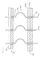
- the vertical probe card comprises a main substrate composed of more than ten layers forming conductive patterns, a probe having a V-bend in the middle, and a probe support provided beneath the main substrate, and having an upper guide plate and a lower guide plate at both sides of the bend.
- the junction at the lower end of the probe is soldered to the conductive pattern of the surface by way of a through-hole opened in the main substrate.
- Through-holes for passing the probe are opened in the upper guide plate and lower guide plate.
- the two-dimensional configuration of the probe is designed corresponding to the layout of electrode pads of the LSI chip to be measured.
- the invention is created in the light of the above circumstances, and it is hence an object thereof to present a vertical probe card capable of measuring the modern LSI chips smaller in size and higher in density and integration, and being reusable, if a probe is broken.
- the vertical probe card of the invention is a vertical probe card having vertical probes for use in measurement of electric characteristics of the objects of measurement, comprising a main substrate forming conductive patterns, a plurality of probes drooping vertically from the main substrate, and a probe support provided at the back side of the main substrate for supporting the probes, in which the probe support is disposed parallel to the main substrate, and has an upper guide plate and a lower guide plate for supporting the probes by passing the through-holes opened in each, and the lower guide plate is composed of a plurality of substrates laminated separably.
- a probe card in an embodiment of the invention is a vertical probe card having vertical probes 100, being used in measurement of electric characteristics of an LSI chip 610 to be measured as shown in Fig. 1 and others, comprising a main substrate 300 on which are formed conductive patterns 310, a plurality of probes 100 extending vertically from the main substrate 300, and a probe support 200 provided at the back side of the main substrate 300 for supporting the probes 100, in which the probe support 200 is disposed parallel to the main substrate 300, and has an upper guide plate 210 and a lower guide plate 220 for supporting the probes 100 by passing the through-holes 211, 221 opened in each, and the lower guide plate 220 is composed of a plurality of (three in the drawing) substrates 220A, 220B, 220C laminated separately.
- the main substrate 300 is a substrate on which are formed conductive patterns 310 on the surface. Plural through-holes 320 are opened in this main substrate 300.
- the through-holes 320 correspond to the layout of electrode pads 611 of an LSI chip 610.
- the through-holes 320 are the portions in which the junctions at the rear ends of the probes 100 are inserted, and the inserted junctions are electrically connected to the conductive patterns 310 by thin wires 330.
- the probe support 200 includes a member 250 extending perpendicularly from the side of the main substrate 300 not carrying the conductive pattern, and the upper guide plate 210 and lower guide plate 220 attached to this extending member 250 at a specific interval.
- Through-holes 211 and 221 pass through the upper guide plate 210 and lower guide plate 220 respectively.
- the through-holes 211, 221 correspond to the layout of electrode pads 611 of the LSI chip 610. Therefore, the through-hole 211 of the upper guide plate 210, and the corresponding through-hole 221 of the lower guide plate 220 and also the through-hole 320 of the main substrate 300 are positioned on a same vertical line.
- the probes 100 are fixed by an insulating synthetic resin 212 extending over the upper surface of the upper guide plate 210, for example, silicone rubber, as shown in Fig. 2 and others.
- the lower guide plate 220 is, as shown in Figs. 2-5, composed of three substrates 220A, 220B, 220C which are laminated separately.
- the three substrates 220A, 220B, 220C are laminated in a state fixed by bolts 222.
- the probe 100 forms a pointed contact part 110 at the leading end, and also has a pointed junction at the rear end.
- the probe 100 is, for example, made of a processed tungsten thin wire, and is about 50 to 150 ⁇ m in diameter.
- This probe 100 has a curved bend 130.
- the bend 130 is deflected at the time of overdrive as mentioned below, and elastically holds a specified contact pressure together with the electrode pad 611 of the LSI chip 610.
- the probe card having such configuration measures the electric characteristics of the LSI chip 610 in the following manner.
- Plural LSI chips 610 in a wafer state are sucked in vacuum on the upper surface of the table 700.
- the probe card is lowered toward the table 700, and the contact parts 110 of all probes 100 are brought into contact with the electrode pads 611 of each LSI chip 610. Further, after the contact parts 110 contact with the electrode pads 611, the probe card is lowered in order to maintain a specified contact pressure (overdrive).
- probe 100 is broken. Most breakage accidents of probe 100 are breakage of the leading end contact part 110 as shown in Fig. 3. That is, the broken probe 100 is shortened in length, and is not suitable to contact with the electrode pad 611. In such a case, the substrate 220A of the lowest side of the lower guide plate 220 is peeled off. As a result, most intact probes 110 project further by the thickness of the substrate 220A separated from the lower guide plate 220. On the other hand, the probe 100 of which leading end contact part 110 is broken is polished in the leading end, and is projected again sufficiently to work as contact part 110.
- the bolts 222 for fixing the three substrates 220A, 220B, 220C to produce the lower guide plate 220 are loosened.
- all probes 100 are polished.
- the polishing process consists of two steps, that is, flattening for aligning the length of all probes 100, and sharpening for forming sharp contact parts 110 at the leading ends of all probes 100 aligned in length.
- the polished probes 100 are shorter by the polished portion, but since all contact parts 110 are aligned on the same plane, they can be reused.
- the lower guide plate 220 is composed of three substrates 220A, 220B, 220C, two polishing sessions are possible.
- the lower guide plate 220 is composed of three substrates 220A, 220B, 220C, but it may be also composed of two or four or more substrates.
- the vertical probe card of the invention is a vertical probe card having vertical probes for use in measurement of electric characteristics of the objects of measurement, comprising a main substrate forming conductive patterns, a plurality of probes drooping vertically from the main substrate, and a probe support provided at the back side of the main substrate for supporting the probes, in which the probe support is disposed parallel to the main substrate, and has an upper guide plate and a lower guide plate for supporting the probes by passing the through-holes opened in each, and the lower guide plate is composed of a plurality of substrates laminated separably.
- the vertical probe card can be reused without replacing the broken probe.
Landscapes
- Physics & Mathematics (AREA)
- General Physics & Mathematics (AREA)
- Testing Or Measuring Of Semiconductors Or The Like (AREA)
- Measuring Leads Or Probes (AREA)
- Testing Of Individual Semiconductor Devices (AREA)
Applications Claiming Priority (2)
| Application Number | Priority Date | Filing Date | Title |
|---|---|---|---|
| JP2000241903A JP3486841B2 (ja) | 2000-08-09 | 2000-08-09 | 垂直型プローブカード |
| JP2000241903 | 2000-08-09 |
Publications (3)
| Publication Number | Publication Date |
|---|---|
| EP1197756A2 true EP1197756A2 (de) | 2002-04-17 |
| EP1197756A3 EP1197756A3 (de) | 2003-08-06 |
| EP1197756B1 EP1197756B1 (de) | 2005-03-16 |
Family
ID=18733017
Family Applications (1)
| Application Number | Title | Priority Date | Filing Date |
|---|---|---|---|
| EP01306788A Expired - Lifetime EP1197756B1 (de) | 2000-08-09 | 2001-08-08 | Sondenkarte zur Prüfung integrierter Schaltungen |
Country Status (6)
| Country | Link |
|---|---|
| US (1) | US6853208B2 (de) |
| EP (1) | EP1197756B1 (de) |
| JP (1) | JP3486841B2 (de) |
| KR (1) | KR100395064B1 (de) |
| DE (1) | DE60109386D1 (de) |
| TW (1) | TWI223072B (de) |
Cited By (6)
| Publication number | Priority date | Publication date | Assignee | Title |
|---|---|---|---|---|
| EP1524529A1 (de) * | 2003-10-13 | 2005-04-20 | Technoprobe S.p.A | Prüfnadel für einen Prüfkopf mit vertikalen Prüfnadeln für integrierte Halbleitergeräte |
| WO2006109328A1 (en) * | 2005-04-12 | 2006-10-19 | Technoprobe S.P.A. | Contact probe for a testing head having vertical probes for semiconductor integreted electronic devices |
| CN100547406C (zh) * | 2006-08-29 | 2009-10-07 | 旺矽科技股份有限公司 | 垂直式高频探针卡 |
| ITMI20102125A1 (it) * | 2010-11-16 | 2012-05-17 | Technoprobe Spa | Sonda di contattatura per testa di misura di dispositivi elettronici |
| ITMI20130561A1 (it) * | 2013-04-09 | 2014-10-10 | Technoprobe Spa | Testa di misura di dispositivi elettronici |
| IT201600079679A1 (it) * | 2016-07-28 | 2018-01-28 | Technoprobe Spa | Scheda di misura di dispositivi elettronici |
Families Citing this family (49)
| Publication number | Priority date | Publication date | Assignee | Title |
|---|---|---|---|---|
| MY137372A (en) * | 2003-11-14 | 2009-01-30 | Wentworth Lab Inc | Die design with integrated assembly aid |
| US9097740B2 (en) * | 2004-05-21 | 2015-08-04 | Formfactor, Inc. | Layered probes with core |
| US7733101B2 (en) * | 2004-05-21 | 2010-06-08 | Microprobe, Inc. | Knee probe having increased scrub motion |
| US9476911B2 (en) | 2004-05-21 | 2016-10-25 | Microprobe, Inc. | Probes with high current carrying capability and laser machining methods |
| USRE43503E1 (en) | 2006-06-29 | 2012-07-10 | Microprobe, Inc. | Probe skates for electrical testing of convex pad topologies |
| US7759949B2 (en) * | 2004-05-21 | 2010-07-20 | Microprobe, Inc. | Probes with self-cleaning blunt skates for contacting conductive pads |
| US8988091B2 (en) | 2004-05-21 | 2015-03-24 | Microprobe, Inc. | Multiple contact probes |
| US7659739B2 (en) * | 2006-09-14 | 2010-02-09 | Micro Porbe, Inc. | Knee probe having reduced thickness section for control of scrub motion |
| JP4201739B2 (ja) | 2004-05-31 | 2008-12-24 | 独立行政法人物質・材料研究機構 | プローブ |
| US7279911B2 (en) * | 2005-05-03 | 2007-10-09 | Sv Probe Pte Ltd. | Probe card assembly with dielectric structure |
| JP4743850B2 (ja) * | 2005-07-07 | 2011-08-10 | 金井 宏彰 | 垂直型プロ−ブピン |
| US7511510B2 (en) * | 2005-11-30 | 2009-03-31 | International Business Machines Corporation | Nanoscale fault isolation and measurement system |
| US7649367B2 (en) | 2005-12-07 | 2010-01-19 | Microprobe, Inc. | Low profile probe having improved mechanical scrub and reduced contact inductance |
| TWI271525B (en) * | 2006-01-17 | 2007-01-21 | Chipmos Technologies Inc | Probe head with vertical probes, method for manufacturing the probe head, and probe card using the probe head |
| US7312617B2 (en) | 2006-03-20 | 2007-12-25 | Microprobe, Inc. | Space transformers employing wire bonds for interconnections with fine pitch contacts |
| JP2007303826A (ja) * | 2006-05-08 | 2007-11-22 | Tokyo Electron Ltd | プローブ |
| US7683645B2 (en) * | 2006-07-06 | 2010-03-23 | Mpi Corporation | High-frequency probe card and transmission line for high-frequency probe card |
| US7400156B2 (en) * | 2006-09-06 | 2008-07-15 | Mjc Probe Incorporation | Vertical probe device |
| US8907689B2 (en) * | 2006-10-11 | 2014-12-09 | Microprobe, Inc. | Probe retention arrangement |
| US7786740B2 (en) * | 2006-10-11 | 2010-08-31 | Astria Semiconductor Holdings, Inc. | Probe cards employing probes having retaining portions for potting in a potting region |
| DE202007016398U1 (de) * | 2006-11-27 | 2008-02-21 | Feinmetall Gmbh | Kontaktiervorrichtung zum Kontaktieren eines zu prüfenden elektrischen Prüflings |
| KR101306654B1 (ko) * | 2006-12-11 | 2013-09-10 | (주) 미코에스앤피 | 프로브 모듈 및 그 제조 방법, 상기 프로브 모듈을 갖는프로브 카드 및 그 제조 방법 |
| KR100847507B1 (ko) * | 2007-02-07 | 2008-07-21 | 윌테크놀러지(주) | 니들 및 이를 구비한 프로브 카드 |
| US7514948B2 (en) * | 2007-04-10 | 2009-04-07 | Microprobe, Inc. | Vertical probe array arranged to provide space transformation |
| US7554348B2 (en) * | 2007-06-29 | 2009-06-30 | Wentworth Laboratories, Inc. | Multi-offset die head |
| KR101329814B1 (ko) * | 2007-07-24 | 2013-11-15 | 주식회사 코리아 인스트루먼트 | 프로브 카드 |
| US8723546B2 (en) * | 2007-10-19 | 2014-05-13 | Microprobe, Inc. | Vertical guided layered probe |
| US7671610B2 (en) * | 2007-10-19 | 2010-03-02 | Microprobe, Inc. | Vertical guided probe array providing sideways scrub motion |
| US8230593B2 (en) * | 2008-05-29 | 2012-07-31 | Microprobe, Inc. | Probe bonding method having improved control of bonding material |
| US8073019B2 (en) * | 2009-03-02 | 2011-12-06 | Jian Liu | 810 nm ultra-short pulsed fiber laser |
| TW201111790A (en) * | 2009-09-16 | 2011-04-01 | Probeleader Co Ltd | High-frequency vertical probe card structure |
| TWI417549B (zh) * | 2010-07-12 | 2013-12-01 | Mpi Corp | The method of making the probe head of the vertical probe card and its composite board |
| CN102346201B (zh) * | 2010-07-26 | 2015-06-17 | 旺矽科技股份有限公司 | 垂直式探针卡的探针头及其复合板的制作方法 |
| US8963567B2 (en) | 2011-10-31 | 2015-02-24 | International Business Machines Corporation | Pressure sensing and control for semiconductor wafer probing |
| US20140139247A1 (en) * | 2012-11-21 | 2014-05-22 | Youngseok Oh | Interposer apparatus and methods |
| KR101476683B1 (ko) * | 2013-05-08 | 2014-12-26 | (주) 루켄테크놀러지스 | 수직형 필름 타입 프로브 카드 |
| JP6245876B2 (ja) * | 2013-07-26 | 2017-12-13 | 株式会社日本マイクロニクス | プローブカード |
| TWI522628B (zh) * | 2013-12-13 | 2016-02-21 | Mpi Corp | Electrical detection device |
| KR101467381B1 (ko) * | 2014-01-27 | 2014-12-02 | 윌테크놀러지(주) | 반도체 검사장치 |
| KR101421051B1 (ko) | 2014-01-27 | 2014-07-22 | 윌테크놀러지(주) | 반도체 검사장치 |
| TWI521212B (zh) * | 2014-03-10 | 2016-02-11 | A method and a method of assembling a vertical probe device, and a vertical probe device | |
| TW201537181A (zh) * | 2014-03-25 | 2015-10-01 | Mpi Corp | 垂直式探針裝置及使用於該垂直式探針裝置之支撐柱 |
| TWI553316B (zh) * | 2014-04-21 | 2016-10-11 | 旺矽科技股份有限公司 | 探針頭及探針 |
| JP6749408B2 (ja) * | 2016-10-31 | 2020-09-02 | 京セラ株式会社 | プローブカード用基板、プローブカード、および検査装置 |
| JP7511325B2 (ja) * | 2018-12-10 | 2024-07-05 | プローブイノベーション株式会社 | 垂直プローブと垂直プローブ用治具 |
| CN110865295A (zh) * | 2019-10-30 | 2020-03-06 | 武汉光庭信息技术股份有限公司 | 一种板载ic管脚信号测试治具 |
| EP4261547A1 (de) | 2022-04-12 | 2023-10-18 | Microtest S.p.A. | Prüfkopf mit vertikalen sonden für eine sondenkarte und zugehöriges montageverfahren |
| CN119199206A (zh) * | 2023-06-27 | 2024-12-27 | 迪科特测试科技(苏州)有限公司 | 包含不同长度探针组的探针卡结构 |
| EP4664117A1 (de) | 2024-06-11 | 2025-12-17 | Microtest S.p.A. | Kontaktsonde mit anpassbarer geometrie und entsprechender sondenkopf |
Family Cites Families (13)
| Publication number | Priority date | Publication date | Assignee | Title |
|---|---|---|---|---|
| US4321532A (en) * | 1978-03-16 | 1982-03-23 | Luna L Jack | Repairable spring probe assembly |
| US4931726A (en) * | 1987-06-22 | 1990-06-05 | Hitachi, Ltd. | Apparatus for testing semiconductor device |
| US4901013A (en) * | 1988-08-19 | 1990-02-13 | American Telephone And Telegraph Company, At&T Bell Laboratories | Apparatus having a buckling beam probe assembly |
| IT1243302B (it) * | 1990-06-19 | 1994-05-26 | St Microelectronics Srl | Connessione universale multicontatto tra scheda portasonde ews e scheda di prova per una stazione di collaudo su fetta di dispositivi a semiconduttore. |
| US5128612A (en) * | 1990-07-31 | 1992-07-07 | Texas Instruments Incorporated | Disposable high performance test head |
| US5325052A (en) * | 1990-11-30 | 1994-06-28 | Tokyo Electron Yamanashi Limited | Probe apparatus |
| US5525911A (en) * | 1993-08-04 | 1996-06-11 | Tokyo Electron Limited | Vertical probe tester card with coaxial probes |
| EP0740160A1 (de) * | 1995-04-24 | 1996-10-30 | Nihon Denshizairyo Kabushiki Kaisha | Vertikal arbeitende Testkarte |
| JP2972595B2 (ja) * | 1996-09-25 | 1999-11-08 | 日本電気ファクトリエンジニアリング株式会社 | プローブカード |
| US5977787A (en) * | 1997-06-16 | 1999-11-02 | International Business Machines Corporation | Large area multiple-chip probe assembly and method of making the same |
| US5952843A (en) * | 1998-03-24 | 1999-09-14 | Vinh; Nguyen T. | Variable contact pressure probe |
| JP3099951B2 (ja) | 1998-11-27 | 2000-10-16 | 日本電子材料株式会社 | 分割型プローブカード |
| US6297657B1 (en) * | 1999-01-11 | 2001-10-02 | Wentworth Laboratories, Inc. | Temperature compensated vertical pin probing device |
-
2000
- 2000-08-09 JP JP2000241903A patent/JP3486841B2/ja not_active Expired - Fee Related
-
2001
- 2001-05-02 TW TW090110480A patent/TWI223072B/zh not_active IP Right Cessation
- 2001-05-10 US US09/851,946 patent/US6853208B2/en not_active Expired - Fee Related
- 2001-05-25 KR KR10-2001-0028810A patent/KR100395064B1/ko not_active Expired - Fee Related
- 2001-08-08 DE DE60109386T patent/DE60109386D1/de not_active Expired - Lifetime
- 2001-08-08 EP EP01306788A patent/EP1197756B1/de not_active Expired - Lifetime
Cited By (13)
| Publication number | Priority date | Publication date | Assignee | Title |
|---|---|---|---|---|
| EP1524529A1 (de) * | 2003-10-13 | 2005-04-20 | Technoprobe S.p.A | Prüfnadel für einen Prüfkopf mit vertikalen Prüfnadeln für integrierte Halbleitergeräte |
| US7301354B2 (en) | 2003-10-13 | 2007-11-27 | Technoprobe S.P.A. | Contact probe for a testing head having vertical probes for semiconductor integrated devices |
| WO2006109328A1 (en) * | 2005-04-12 | 2006-10-19 | Technoprobe S.P.A. | Contact probe for a testing head having vertical probes for semiconductor integreted electronic devices |
| CN100547406C (zh) * | 2006-08-29 | 2009-10-07 | 旺矽科技股份有限公司 | 垂直式高频探针卡 |
| ITMI20102125A1 (it) * | 2010-11-16 | 2012-05-17 | Technoprobe Spa | Sonda di contattatura per testa di misura di dispositivi elettronici |
| WO2014167410A3 (en) * | 2013-04-09 | 2015-04-30 | Technoprobe S.P.A. | Testing head of electronic devices |
| ITMI20130561A1 (it) * | 2013-04-09 | 2014-10-10 | Technoprobe Spa | Testa di misura di dispositivi elettronici |
| KR20150140774A (ko) * | 2013-04-09 | 2015-12-16 | 테크노프로브 에스.피.에이. | 전자 장치의 검사 헤드 |
| US9829508B2 (en) * | 2013-04-09 | 2017-11-28 | Technoprobe S.P.A. | Testing head of electronic devices |
| IT201600079679A1 (it) * | 2016-07-28 | 2018-01-28 | Technoprobe Spa | Scheda di misura di dispositivi elettronici |
| WO2018019863A1 (en) * | 2016-07-28 | 2018-02-01 | Technoprobe S.P.A. | Probe card for electronic devices |
| KR20190034502A (ko) * | 2016-07-28 | 2019-04-02 | 테크노프로브 에스.피.에이. | 전자 장치를 위한 프로브 카드 |
| TWI684011B (zh) * | 2016-07-28 | 2020-02-01 | 義大利商探針科技公司 | 電子裝置用探針卡 |
Also Published As
| Publication number | Publication date |
|---|---|
| KR100395064B1 (ko) | 2003-08-21 |
| TWI223072B (en) | 2004-11-01 |
| EP1197756B1 (de) | 2005-03-16 |
| EP1197756A3 (de) | 2003-08-06 |
| JP3486841B2 (ja) | 2004-01-13 |
| DE60109386D1 (de) | 2005-04-21 |
| US6853208B2 (en) | 2005-02-08 |
| KR20020013377A (ko) | 2002-02-20 |
| JP2002055119A (ja) | 2002-02-20 |
| US20020041189A1 (en) | 2002-04-11 |
Similar Documents
| Publication | Publication Date | Title |
|---|---|---|
| EP1197756B1 (de) | Sondenkarte zur Prüfung integrierter Schaltungen | |
| KR100430208B1 (ko) | 시험조립체 | |
| US5073117A (en) | Flip-chip test socket adaptor and method | |
| EP0475050A2 (de) | Flexibles Band mit Prüfkontakten | |
| US6515358B1 (en) | Integrated passivation process, probe geometry and probing process | |
| US20100134126A1 (en) | Probe and method for manufacturing the same | |
| JPWO2007029422A1 (ja) | 半導体装置の検査装置及び電源供給ユニット | |
| KR100374732B1 (ko) | 반도체웨이퍼접촉시스템및반도체웨이퍼접촉방법 | |
| TW201029087A (en) | Method and apparatus for testing a semiconductor wafer | |
| US7332922B2 (en) | Method for fabricating a structure for making contact with a device | |
| CN100499056C (zh) | 半导体集成电路器件的制造方法 | |
| CN212845494U (zh) | 电连接装置 | |
| US5940680A (en) | Method for manufacturing known good die array having solder bumps | |
| JPH06313788A (ja) | 半導体チップテスト用ソケット | |
| JP2571516B2 (ja) | プローブカード | |
| US7112975B1 (en) | Advanced probe card and method of fabricating same | |
| JP3129641B2 (ja) | テスト用コンタクトピンの製造方法 | |
| EP0654672A2 (de) | Testvorrichtung für integrierte Schaltungen | |
| JPH1164389A (ja) | バンプ型コンタクタ及びバンプ型コンタクタ用接触子の製造方法 | |
| JP2571517B2 (ja) | プローブカード | |
| JP3051599B2 (ja) | 半導体チップテスト用ソケット | |
| JPH11142438A (ja) | プローブ及びこのプローブを用いたプローブカード | |
| KR101273970B1 (ko) | 프로브의 탐침 및 프로브의 제조방법 | |
| JP2001201516A (ja) | プローブ要素の製作方法及び装置並びに窪み形成装置 | |
| JP2002131337A (ja) | 半導体素子検査基板 |
Legal Events
| Date | Code | Title | Description |
|---|---|---|---|
| PUAI | Public reference made under article 153(3) epc to a published international application that has entered the european phase |
Free format text: ORIGINAL CODE: 0009012 |
|
| 17P | Request for examination filed |
Effective date: 20010906 |
|
| AK | Designated contracting states |
Kind code of ref document: A2 Designated state(s): AT BE CH CY DE DK ES FI FR GB GR IE IT LI LU MC NL PT SE TR |
|
| AX | Request for extension of the european patent |
Free format text: AL;LT;LV;MK;RO;SI |
|
| PUAL | Search report despatched |
Free format text: ORIGINAL CODE: 0009013 |
|
| AK | Designated contracting states |
Designated state(s): AT BE CH CY DE DK ES FI FR GB GR IE IT LI LU MC NL PT SE TR |
|
| AX | Request for extension of the european patent |
Extension state: AL LT LV MK RO SI |
|
| AKX | Designation fees paid |
Designated state(s): DE FR GB IT NL |
|
| 17Q | First examination report despatched |
Effective date: 20040324 |
|
| GRAP | Despatch of communication of intention to grant a patent |
Free format text: ORIGINAL CODE: EPIDOSNIGR1 |
|
| GRAS | Grant fee paid |
Free format text: ORIGINAL CODE: EPIDOSNIGR3 |
|
| GRAA | (expected) grant |
Free format text: ORIGINAL CODE: 0009210 |
|
| AK | Designated contracting states |
Kind code of ref document: B1 Designated state(s): DE FR GB IT NL |
|
| PG25 | Lapsed in a contracting state [announced via postgrant information from national office to epo] |
Ref country code: NL Free format text: LAPSE BECAUSE OF FAILURE TO SUBMIT A TRANSLATION OF THE DESCRIPTION OR TO PAY THE FEE WITHIN THE PRESCRIBED TIME-LIMIT Effective date: 20050316 Ref country code: IT Free format text: LAPSE BECAUSE OF FAILURE TO SUBMIT A TRANSLATION OF THE DESCRIPTION OR TO PAY THE FEE WITHIN THE PRESCRIBED TIME-LIMIT;WARNING: LAPSES OF ITALIAN PATENTS WITH EFFECTIVE DATE BEFORE 2007 MAY HAVE OCCURRED AT ANY TIME BEFORE 2007. THE CORRECT EFFECTIVE DATE MAY BE DIFFERENT FROM THE ONE RECORDED. Effective date: 20050316 |
|
| REG | Reference to a national code |
Ref country code: GB Ref legal event code: FG4D |
|
| REG | Reference to a national code |
Ref country code: IE Ref legal event code: FG4D |
|
| REF | Corresponds to: |
Ref document number: 60109386 Country of ref document: DE Date of ref document: 20050421 Kind code of ref document: P |
|
| PG25 | Lapsed in a contracting state [announced via postgrant information from national office to epo] |
Ref country code: DE Free format text: LAPSE BECAUSE OF FAILURE TO SUBMIT A TRANSLATION OF THE DESCRIPTION OR TO PAY THE FEE WITHIN THE PRESCRIBED TIME-LIMIT Effective date: 20050617 |
|
| PG25 | Lapsed in a contracting state [announced via postgrant information from national office to epo] |
Ref country code: GB Free format text: LAPSE BECAUSE OF NON-PAYMENT OF DUE FEES Effective date: 20050808 |
|
| NLV1 | Nl: lapsed or annulled due to failure to fulfill the requirements of art. 29p and 29m of the patents act | ||
| ET | Fr: translation filed | ||
| PLBE | No opposition filed within time limit |
Free format text: ORIGINAL CODE: 0009261 |
|
| STAA | Information on the status of an ep patent application or granted ep patent |
Free format text: STATUS: NO OPPOSITION FILED WITHIN TIME LIMIT |
|
| 26N | No opposition filed |
Effective date: 20051219 |
|
| GBPC | Gb: european patent ceased through non-payment of renewal fee |
Effective date: 20050808 |
|
| PGFP | Annual fee paid to national office [announced via postgrant information from national office to epo] |
Ref country code: FR Payment date: 20090717 Year of fee payment: 9 |
|
| REG | Reference to a national code |
Ref country code: FR Ref legal event code: ST Effective date: 20110502 |
|
| PG25 | Lapsed in a contracting state [announced via postgrant information from national office to epo] |
Ref country code: FR Free format text: LAPSE BECAUSE OF NON-PAYMENT OF DUE FEES Effective date: 20100831 |