EP1174852B1 - Picture image display device and method of driving the same - Google Patents
Picture image display device and method of driving the same Download PDFInfo
- Publication number
- EP1174852B1 EP1174852B1 EP01114025.8A EP01114025A EP1174852B1 EP 1174852 B1 EP1174852 B1 EP 1174852B1 EP 01114025 A EP01114025 A EP 01114025A EP 1174852 B1 EP1174852 B1 EP 1174852B1
- Authority
- EP
- European Patent Office
- Prior art keywords
- terminal
- differential amplifier
- switch
- output
- display
- Prior art date
- Legal status (The legal status is an assumption and is not a legal conclusion. Google has not performed a legal analysis and makes no representation as to the accuracy of the status listed.)
- Expired - Lifetime
Links
Images


Classifications
-
- G—PHYSICS
- G09—EDUCATION; CRYPTOGRAPHY; DISPLAY; ADVERTISING; SEALS
- G09G—ARRANGEMENTS OR CIRCUITS FOR CONTROL OF INDICATING DEVICES USING STATIC MEANS TO PRESENT VARIABLE INFORMATION
- G09G3/00—Control arrangements or circuits, of interest only in connection with visual indicators other than cathode-ray tubes
- G09G3/20—Control arrangements or circuits, of interest only in connection with visual indicators other than cathode-ray tubes for presentation of an assembly of a number of characters, e.g. a page, by composing the assembly by combination of individual elements arranged in a matrix no fixed position being assigned to or needed to be assigned to the individual characters or partial characters
- G09G3/34—Control arrangements or circuits, of interest only in connection with visual indicators other than cathode-ray tubes for presentation of an assembly of a number of characters, e.g. a page, by composing the assembly by combination of individual elements arranged in a matrix no fixed position being assigned to or needed to be assigned to the individual characters or partial characters by control of light from an independent source
- G09G3/36—Control arrangements or circuits, of interest only in connection with visual indicators other than cathode-ray tubes for presentation of an assembly of a number of characters, e.g. a page, by composing the assembly by combination of individual elements arranged in a matrix no fixed position being assigned to or needed to be assigned to the individual characters or partial characters by control of light from an independent source using liquid crystals
- G09G3/3611—Control of matrices with row and column drivers
- G09G3/3685—Details of drivers for data electrodes
- G09G3/3688—Details of drivers for data electrodes suitable for active matrices only
-
- G—PHYSICS
- G09—EDUCATION; CRYPTOGRAPHY; DISPLAY; ADVERTISING; SEALS
- G09G—ARRANGEMENTS OR CIRCUITS FOR CONTROL OF INDICATING DEVICES USING STATIC MEANS TO PRESENT VARIABLE INFORMATION
- G09G2310/00—Command of the display device
- G09G2310/02—Addressing, scanning or driving the display screen or processing steps related thereto
- G09G2310/0264—Details of driving circuits
- G09G2310/027—Details of drivers for data electrodes, the drivers handling digital grey scale data, e.g. use of D/A converters
-
- G—PHYSICS
- G09—EDUCATION; CRYPTOGRAPHY; DISPLAY; ADVERTISING; SEALS
- G09G—ARRANGEMENTS OR CIRCUITS FOR CONTROL OF INDICATING DEVICES USING STATIC MEANS TO PRESENT VARIABLE INFORMATION
- G09G2310/00—Command of the display device
- G09G2310/02—Addressing, scanning or driving the display screen or processing steps related thereto
- G09G2310/0264—Details of driving circuits
- G09G2310/0291—Details of output amplifiers or buffers arranged for use in a driving circuit
Definitions
- the present invention relates to a liquid crystal (hereinbelow, will be referred to as LC) picture image display device which, in particular, permits a picture image display of a high quality.
- LC liquid crystal
- Fig. 11 is a structural diagram of an offset cancel buffer circuit in a low temperature poly-Si drive circuit used for a conventional TFT LC panel drive.
- An analog input signal Vin is buffered by a negative feed back differential amplifier circuit 155 and is output as an analog output Vout to a TFT LC panel.
- Two negative feed back routes, one via switch 153 and the other via a switch 152 are provided, and the route via the switch 152 is routed through a capacitor 151. Further, from a junction between the switch 152 and the capacitor 151 a wiring is connected to the input portion Vin via a switch 154.
- Positive and Negative input portions of the differential amplifier circuit 155 are constituted by a low temperature poly-Si TFT, however, since the element characteristics of a low temperature poly-Si TFT generally fluctuate largely in comparison with a single crystal MOS transistor, therefore, if a simple feed back is effected, a large fluctuation in output offset voltage is caused for every buffer circuit in a voltage follower circuit, an uneven brightness in a form of vertical stripes is induced on an LC panel display. Therefore, in the present conventional circuit, in order to cancel the offset voltage, an offset cancel circuit is introduced. During the former half of the horizontal scanning period the switches 153 and 154 are turned on and the switch 152 is turned off.
- an output offset voltage of the differential amplifier circuit 155 with a negative feed back loop is stored in the capacitor 151.
- the switches 153 and 154 are turned off and the switch 152 is turned on.
- the capacitor 151 which stores the output offset voltage is added in series, the output offset voltage is subtracted by the differential amplifier circuit 155. Namely, with thus structured circuit, the output offset voltage can be canceled.
- the switch 153 FET (Field Effect Transistor) switch
- the switch 153 becomes a new major ground of fluctuation in output offset voltage, and in order to further enhance an output voltage accuracy of the offset cancel circuit the above new major ground has to be resolved which will be explained likely by making use of Fig. 11 .
- the switches 153 and 154 are turned on and after causing to store the output offset voltage of the differential amplifier circuit 151 into the capacitor 151 having the capacitance Cm, the switches 153 and 154 are turned off. It is well known that at this moment the. TFTs constituting the respective switches discharge to their sides of source and drain feed through charges. As the result thereof, ql among the feed through charges of the switch 153 is added to the charge originally stored in the capacitor 151 having the capacitance Cm to modulate the voltage between the capacitor 151.
- the open gain G of the differential amplifier circuit 155 is generally designed in an extremely large value. Therefore, if a sufficiently large value is assumed for G in equation (1), it is understood that generation of the offset voltage ⁇ Vout determined by (-ql/Cm) due to the feed through charge by the switch 153 cannot be avoided. Further, in this instance, the charge q2 caused by the switch 153 affects no important effect.
- the new offset voltage ⁇ Vout causes a large problem when enhancing the output voltage accuracy of the buffer circuit. If (-ql/Cm) is a constant value, an external correction is possible. However, the problem to be resolved here is the uneven brightness in a form of vertical stripe shape induced in a displayed picture image on the TFT LC panel due to the fluctuation of q1, an external correction thereof is difficult.
- the offset fluctuation due to the above fluctuation in ql is referred to as "switch feed through offset fluctuation".
- the threshold voltage Vth thereof generally fluctuates about 20mV at maximum as well as the gate size thereof is in a degree of submicron. Therefore, the above "switch feed through offset fluctuation" can be suppressed with a capacitor having a comparatively small Cm.
- a poly crystalline Si-TFT is used for the switch 153, since a crystal grain structure is included in a channel portion and a defect level density of a gate insulation film boundary is nonuniform, the threshold voltage Vth fluctuates from several 100mV to about 1V at the maximum.
- the switch feed through charge q1 is primarily proportional to a channel charge Cg ⁇ (Vg-Vth).
- Cg is a gate capacitance determined by the gate area, the gate insulation film thickness and the gate insulation film dielectric constant. Accordingly, the fluctuation in the threshold voltage Vth and the gate area as they are directly reflects to the switch feed through charge q1.
- the fluctuation in feed through charge ql of the offset cancel use switch connected to the input of the differential amplifier circuit induces the new offset voltage fluctuation as referred to as "switch feed through offset fluctuation" and in order to further enhance the output voltage accuracy of the buffer circuit a new counter measure therefor is necessary.
- the switch 153 which caused the above explained problem of the feed through charges is constituted by such as n type TFT, p type TFT and CMOS TFT, it will be apparent that the same problem is caused in view of the "fluctuation" in the feed through charges.
- a picture invention as defined in claim 1. It comprises a liquid crystal opposing electrode to which a predetermined voltage is applied; a pixel electrode which is provided so as to form a liquid crystal capacitor with the liquid crystal opposing electrode; a pixel switch connected in series with the pixel electrode; a plurality of display pixels arranged in a matrix shape for performing picture image display; a picture image signal voltage generation means which outputs a first analog picture image signal voltage based on picture image data to be displaced; a group of output impedance conversion means using a semiconductor element to which the first analog picture image signal voltage is inputted and which outputs a second analog picture image signal voltage with a lower output impedance than that of the picture image signal voltage generation means; an offset cancel capacitor which is provided in the output impedance conversion means for canceling an output offset fluctuation of the second analog picture image signal voltages due to fluctuation of the semiconductor characteristic in the group of the respective output impedance conversion means and of which one terminal is connected to a voltage input terminal of the output impedance conversion means
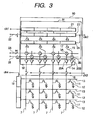
- Fig. 3 is a structural diagram a poly crystalline Si-TFT LC display panel representing the present embodiment.
- Display pixels each of which is constituted by a LC capacitor 12 formed between a pixel electrode and a LC opposing electrode applied of a predetermined voltage and a pixel TFT 11 connected to the LC capacitor 12, are arranged in a matrix shape and constitute a picture image display region.
- the gate of the pixel TFT 11 is connected to a gate line drive circuit 10 via a gate line 13.
- the drain of the pixel TFT 11 is connected to a signal line drive circuit 90 via.a signal line 7. More specifically, the drain electrode of the pixel TFT 11 is connected via the signal line 7 to an analog buffer output switch 16 in the signal line drive circuit 90.
- the other end of the analog buffer output switch 16 is connected via a gradation change-over switch 14 to an output terminal of either of analog buffers 20A and 20B and the input terminals of the analog buffers 20A and 20B are respectively connected to gradation selecting switches 3A and 3B.
- either of the analog buffers 20A and 20B and either of the gradation selecting switches 3A and 3B are selected by the gradation change-over switches 14 and 15.
- the gradation selecting switches 3A and 3B are constituted as a multiplexer and function as a decoder of a D/A converter through connecting a predetermined one of gradation power source lines 2A and 2B selected by a gradation selecting line 17 to the output thereof. Further, in Fig.
- a portion constituted by a latch address selection circuit 21, a primary latch circuit 23, a secondary latch circuit 24 and the gradation selecting switches 3A and 3B is a picture image signal voltage generation unit 91 and a portion constituted by the analog buffers 20A and 20B forms an output impedance conversion means 92 in group.
- the gradation power source lines 2A and 2B are respectively constituted by 64 pieces of parallel wiring lines to which respectively different gradation voltages are applied.
- the gradation selecting line 17 is outputted from the primary latch circuit 23 via the secondary latch circuit 24, and to the primary latch circuit 23 a digital input line 22 and the lath address selection circuit 22 are inputted.
- the above respective circuit blocks are constituted on a glass substrate by making use of poly-crystalline Si-TFT elements, and herein the respective switches use CMOS switches constituted by making use of poly crystalline Si-TFTs. Further, in the present embodiment, in order to simplify explanation a conventional structure necessary for forming a TFT panel such structures as for a color filter and for a back light are omitted.
- the picture image display data inputted in the digital data input line 22 are latched in the primary latch circuit 23 having address selected by the latch address selection circuit 21.
- these picture image display data are collectively transferred from the primary latch circuit 23 to the secondary latch circuit 24 and during the subsequent horizontal scanning period the secondary latch circuit 24 outputs these picture image data to the gradation selecting line 17.
- the gradation selecting switches 3A and 3B constituted by decode switches in group supply, depending on the content of the gradation selecting line 17, a predetermined analog picture image voltage from the gradation power source lines 2A and 2B to the analog buffers 20A and 20B.
- the analog buffers 20A and 20B supply the picture image signal voltage corresponding to the supplied picture image signal voltage via the analog buffer output switch 16 to the signal line 7.
- Roles of the analog buffers 20A and 20B are to reduce the output impedance at this moment lower than the output impedance in the gradation selecting switches 3A and 3B so as to enhance writing speed of the signal voltage into the signal line 7 as well as to prevent a possible cross talk such as by capacitive coupling of the signal lines 7 each other possibly caused by outputting the picture image signal voltage with a low impedance.
- the analog buffers 20A and 20B are provided with, in addition to the offset cancel function for compensating the offset voltage fluctuation by the analog buffers themselves which will be explained later, a function of canceling "switch feed through offset fluctuation" due to the feed through charges caused by the offset cancel circuit.
- the picture image signal voltage with no offset fluctuation inputted into the signal line 7 is written into a predetermined LC capacitor 12, when the gate line drive circuit 10 turns on pixel TFTs 11 in a predetermined line via a gate line 13.
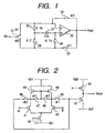
- Fig. 1 is a structure diagram of an analog buffer 20 which includes the above explained offset cancel function and switch feed through offset cancel function.
- Input terminals of the analog buffer 20 are coupled to a change-over switch 31 which changes over depending on phases ⁇ 1 and ⁇ 2.
- One stationary terminal of the change-over switch 31 is connected to a switch 35 which is turned on by a clock cl ⁇ 1b, a switch 32 which is turned on by the phase ⁇ 2 and one of two input terminals of a differential amplifier 30, and the other stationary terminal of the change-over switch is connected to a switch 36 which is turned on by a clock cl ⁇ 2, a change-over witch 34 which is turned on by a clock cl ⁇ 1a and a switch 33 which is turned on by the phase ⁇ 1.
- the other input terminal of the differential amplifier 30 is connected to the change-over switch 34 which is turned on by a clock cl ⁇ 1a and a cancel capacitor 37 of which other terminal is connected to the switch 35 which is turned on by a clock cl ⁇ 1b and the switch 36 which is turned on by a clock cl ⁇ 2.
- the output terminal of the differential amplifier 30 is connected to the output terminal of the analog buffer 20 as well as connected to the switch 32 which is turned on by the phase ⁇ 2 and the switch 33 which is turned on by the phase ⁇ 1.
- the input terminals A and B of the differential amplifier 30 as illustrated in the drawing are changed over to (+, -) when the phase is ⁇ 1 and to (-, +) when the phase is ⁇ 2 as shown in Table 1.
- Fig 2 is a diagram of the differential amplifier 30 having the above explained functions.
- the differential amplifier 30 is constituted by an initial stage differential circuit and a subsequent stage source follower circuit.
- the initial stade differential circuit is constituted by poly crystalline Si-driver TFTs 41 and 42, poly crystalline .
- the subsequent stage source follower circuit which is constituted by a poly crystalline Si-driver TFT 51 and a poly crystalline Si-load TFT 52 which is driven with a predetermined bias, is provided for achieving a matching of a large output current supply with an operating point voltage.
- Vd1, Vs1, Vd2 and Vs2 are respectively voltages of high and low voltage sources for the initial stage differential circuit and for the subsequent stage source follower circuit.
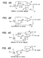
- the operation of the analog buffer 20 will be explained with reference to Figs. 4A through 4D .
- the analog buffer 20 performs memory 1 of offset amount by closing the switches 34 and 35 as shown in Fig. 4A .
- an offset voltage of the analog buffer 20 is inputted between the cancel capacitor 37 having capacitance Cm.
- the switch 36 is closed and subtraction 1 of offset amount is performed as shown in Fig. 4B .
- the cancel capacitor 37 which stores the offset voltage ⁇ V of the analog buffer 20 is inserted into a negative feed back loop of the analog buffer 20, the output voltage of the differential amplifier 30 is reduced by ⁇ V.
- the analog buffer 20 performs memory 2 of offset amount after closing the switches 34 and 35 as shown in Fig. 4C .
- the offset voltage ⁇ V of the analog buffer 20 is inputted between the cancel capacitor 37.
- the subtraction 2 of offset amount is performed after closing the switch 36 as shown in Fig. 4D .
- the cancel capacitor 37 which stores the offset voltage ⁇ V of the analog buffer 20 is inserted to the, positive input terminal of the analog buffer 20, therefore, the output voltage of the differential amplifier 30 is reduced by ⁇ V.
- the offset voltage ⁇ V of the analog buffer 20 is canceled, however, like the above, the switch feed through offset voltage due to the feed through charge ql caused at the positive input terminal side of the differential amplifier 30 when the switch 34 is turned off appears at the output terminal of the analog buffer 20 by the amount of (+q1/Cm).
- the present embodiment is driven with a repeating unit of odd and even two frames.
- the on/off of a switch is illustrated by a high and low levels as indicated in the drawing.
- the high level indicates A
- the low level indicates B so as to correspond to the selected analog buffers 20A and 20B and gradation selecting switches 3A and 3B.
- the phase ⁇ 1 is selected and the gradation change-over switches 14 and 15 are changed over toward selection A.
- a predetermined gate line 13 (pixel TFT 11) which is selected by the gate line drive circuit 10 is turned on, and the switch 36 in the analog buffer 20A is turned off.
- the operation of the offset cancel circuit in the analog buffer 20A is started. Namely, the output of the primary latch circuit 23 is turned on as well as the switches 34 and 35 are turned on and the offset voltage of the differential amplifier 30 is inputted between the cancel capacitor 37.
- the switch 34 and the switch 35 are turned off in this order, of which turn-off order is important in order to remove the influence of the feed through charge caused by the switch 35.
- the fluctuation in feed through charge of the switch 34 connected to the input of the differential amplifier 30 is inputted to a pixel via a signal line 7 as a switch feed through offset voltage in an amount of (-q1A/Cm), wherein a switch feed through charge of the switch 34 in the analog buffer 20A is indicated as q1A.
- a switch feed through charge of the switch 34 in the analog buffer 20A is indicated as q1A.
- a role of the analog buffer output switch 16 is to isolate the output of the analog buffers 20A and 20B from the signal line 7 depending on necessity and to accelerate a built-up of the output of the analog buffers 20A and 20B at the time of the offset voltage cancel operation.
- the writing operation concerned is basically the same as that during the above explained odd frame and positive field period except that the gradation change-over switches 14 and 15 are changed over toward selection B.
- the fluctuation in feed through charge of the switch 34 connected to the input of the differential amplifier 30 is inputted to a pixel via a signal line 7 as a switch feed through offset voltage in an amount of ( -q1B/Cm), wherein the switch feed through charge of the switch 34 in the analog buffer 20B is indicated as qlB.
- the analog buffer 20B is used instead of the analog buffer 20A, it will be apparent that the value q1B is totally independent from the value qlA.
- the writing operation concerned is substantially the same as that during the odd frame and positive field period except that the phase ⁇ 2 is selected.
- the fluctuation in feed through charge of the switch 34 connected to the input of the differential amplifier 30 is inputted to a pixel via a signal line 7 as a switch feed through offset voltage in an amount of (+q1/Cm).
- the respective circuit blocks are constituted on a glass substrate by making use poly crystalline Si-TFT elements.
- a quartz substrate a transparent plastic substrate can be used, and further, by modifying the LC display scheme to a reflection type it is possible to use an opaque substrate including a Si substrate.
- a TFT has an advantage having no substrate bias effect, however, has a disadvantage having a large drain conductance, therefore, although a bias terminal is newly necessitated, in order to ensure a gain of over several 100 times for a differential amplifier circuit, it is effective to use such cascode structure.
- the picture image display data are assumed to be 6 bits and the gradation power source lines are assumed to be 64 pieces of parallel wiring lines to which respectively different gradation voltages are applied, however, it will be apparent if the picture image display data is n bits, the number of the gradation power source lines are 2n pieces of parallel wiring lines to which respectively different gradation voltages are applied.
- the switch groups are constituted by CMOS switches and the pixel TFTs use n type TFT switches, however, any switch structures including p type TFT can be used for the switches in the present embodiment. Further, a variety of structures and layout such as a reflection type display pixel structure can be applied without departing the spirit of the present invention.
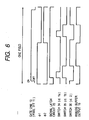
- Fig. 6 is a timing chart of the respective operation pulses according to the present embodiment in a certain row at the time of writing a pixel line during one field period.
- Fig. 6 corresponds to Fig. 5 for the first embodiment, however, in Fig. 6 the explanation with regard to the gradation change-over switches 14 and 15 which change-over positive/negative of the field is omitted. Because, other than the selection between A and B by the gradation change-over switches 14 and 15, the operation of the respective pulses in the positive and negative field is the same in the present embodiment. Further, likely in the present timing chart the on/off of the switches are indicated at high and low levels as illustrated in the drawing.
- the phase ⁇ 1 is selected, subsequently a predetermined gate line 13 (a pixel TFT 11) which is selected by the gate line drive circuit 10 is turned on and the switch 36 is turned off.
- the offset cancel circuit in the analog buffer 20 (likely in the above, the operations in the analog buffers 20A and 20B are basically the same, both are inclusively referred to as an analog buffer 20 in the present embodiment) is started. Namely, the output of the primary latch circuit 23 is turned on as well as the switches 34 and 35 are turned on and the offset voltage of the differential amplifier 30 is inputted between the cancel capacitor 37. Subsequently, the switch 34 and the switch 35 are turned-off in this order.
- the following operation is successively performed. Namely, after the analog buffer output switch 16 once turned off, the phase ⁇ 2 is selected and the output operation of the picture image signal voltage is again repeated. In this instance, the fluctuation in feed through charge of the switch 34 connected to the input of the differential amplifier circuit 30 is inputted to a pixel via a signal line 7 as a switch feed through offset voltage in an amount of (+ql/Cm). Thereafter, through turning off of the gate line 13 (pixel TFT 11) and the analog buffer output switch 16, the writing operation on the pixel for the selected one line is completed.
- Fig. 7 shows a picture image signal voltage which is written to a signal line 7 through the above referred to writing operation.
- an output signal which gradually approaches to (Vin-q1/Cm) is written onto a signal line 7, wherein Vin is a picture image signal voltage to be written onto the signal line 7, and in the drawing ql is indicated to have a negative value.
- an output signal which gradually approaches to (Vin+ql/Cm) is written on the signal line 7.
- the period (t4-t3) is set to a proper value shorter than the period (t2-t1), thereby, a picture image signal voltage VA which is finally written onto the signal line 7 comes close near the value Vin.
- phase change-over ⁇ 1/ ⁇ 2 is performed once in one field, however, the phase change-over can be performed more than once in one field with the same effect.
- Fig. 8 is a circuit structure of an analog buffer 20 according to the present example which includes the offset cancel function and the switch feed through offset cancel function, and likely in the present example, the operations of the analog buffers 20A and 20B are basically the same, the both are referred to as the analog buffer 20.
- An input terminal of the analog buffer 20 is connected to a switch 55 which is turned on by a clock cl ⁇ 1b and a positive input terminal of the differential amplifier 50; further a negative input terminal of the differential amplifier 50 is connected to a switch 54 which is turned on by a clock cl ⁇ 1a1, a switch 58 which is turned on by a clock cl ⁇ 1a2 and a cancel capacitor 57, and the other terminal of the cancel capacitor 57 is connected to the switch 55 which is turned on by a clock cl ⁇ 1b and a switch 56 which is turned on by a clock cl ⁇ 2.
- the output terminal of the differential amplifier 50 is connected to the terminal of the analog buffer 20 as well as at the same time is connected to respective other terminals of the switch 54 which is turned on by a clock cl ⁇ 1a1, of the switch 58 which is turned on by a clock cl ⁇ 1a2 and of the switch 56 which is turned on by a clock cl.2.
- Fig. 9 is a timing chart of the respective operation pulses according to the present example in a certain row at the time of writing a pixel line during one field period and corresponds to Fig. 6 for the second embodiment.
- a predetermined gate line 13 (a pixel TFT 11) which is selected by the gate line drive circuit 10 is turned on and the switch 56 is turned off.
- the offset cancel circuit in the analog buffer 20 is started. Namely, the output of the primary latch circuit 23 is turned on as well as the switches 54, 55 and 58 are turned on and the offset voltage of the differential amplifier 50 is inputted between the cancel capacitor 57. Subsequently, the switch 54, the switch 58 and the switch 55 are turned off in this order.
- the offset voltage of the differential amplifier 50 stored in the cancel capacitor 57 is inputted into the negative feed back loop, thereby, the offset voltage due to TFT non matching of the differential amplifier 50 using poly crystalline Si-TFTs is canceled.
- the analog buffer output switch 16 is turned on, a picture image signal voltage is outputted to a signal line 7 from the analog buffer 20.
- the gate width of the switch 58 which is turned off later is designed to be smaller that the gate width of the switch 54 which is turned off earlier.
- the gate lengths of the both are the same.
- the charging to the cancel capacitor 57 is performed by the switch 54 having a large switch feed through charge and a lower on resistance, further, the reduction of the switch feed through charge is achieved by the switch 58 having a larger on resistance but a smaller switch feed through charge.
- the fluctuation in switch feed through offset voltage can be reduced.
- the gate width of the switch 58 which is turned off later is designed smaller than the gate width of the switch 54 which is turned off earlier.
- the principle of the present invention can be modified in various manners, for example, in such a manner that the gate of the switch 58 which is turned off later is driven by a lower gate voltage than that for the gate of the switch 54 which is turned off earlier.
- Fig. 10 is a structural diagram of a picture image viewer 71 representing a third embodiment of the present invention.
- a wireless interface (I/F) circuit 73 compressed picture image data are inputted from the outside as wireless data based on bluetooth standard, and the output of the wireless I/F circuit 73 is connected via a central processing unit (CPU)/decoder 74 to a frame memory 75. Further, the output of the CPU/decoder 74 is connected via an interface (I/F) circuit 77 provided on a poly crystalline Si LC display panel 76 to a line selection circuit 79 and a data input circuit 78, and a picture image display region 80 is driven by the line selection circuit 79 and the data input circuit 78.
- a picture image viewer 71 is further provided with a power source 82 and a light source 81.
- the structure and operation of the poly crystalline Si LC display panel 76 in the present embodiment are the same as those of the first embodiment.
- the wireless I/F circuit 73 takes in compressed picture image data from the outside and transfers the same to the CPU/decoder 74.
- the CPU/decoder 74 in response to a user's manipulation, drives the picture image viewer depending on necessity or performs decoding process of the compressed picture image data.
- the decoded picture image data are temporarily stored in the frame memory 75 and, according to the command from the CPU/decoder 75, outputs the stored picture image data for displaying picture images and timing pulses to the I/F circuit 77.
- the I/F circuit 77 drives the line selection circuit 79 and the data input circuit 78 to display picture images on the picture image display region while making use of these signals, which is already explained in connection with the first embodiment, therefore, the detailed explanation thereof is omitted.
- the light source is a back light for the LC display, the power source 82 includes a secondary battery and supplies power for driving these entire device.
- the third embodiment can display picture images with a high quality without uneven brightness in a form of vertical stripes due to "switch feed through offset fluctuation" as referred to above based on the compressed picture image data.
- a LC picture image display device which permits a high quality picture image display can be provided.
Landscapes
- Engineering & Computer Science (AREA)
- Chemical & Material Sciences (AREA)
- Crystallography & Structural Chemistry (AREA)
- Physics & Mathematics (AREA)
- Computer Hardware Design (AREA)
- General Physics & Mathematics (AREA)
- Theoretical Computer Science (AREA)
- Liquid Crystal Display Device Control (AREA)
- Control Of Indicators Other Than Cathode Ray Tubes (AREA)
- Liquid Crystal (AREA)
Applications Claiming Priority (2)
| Application Number | Priority Date | Filing Date | Title |
|---|---|---|---|
| JP2000226188A JP4449189B2 (ja) | 2000-07-21 | 2000-07-21 | 画像表示装置およびその駆動方法 |
| JP2000226188 | 2000-07-21 |
Publications (3)
| Publication Number | Publication Date |
|---|---|
| EP1174852A2 EP1174852A2 (en) | 2002-01-23 |
| EP1174852A3 EP1174852A3 (en) | 2002-08-28 |
| EP1174852B1 true EP1174852B1 (en) | 2015-01-14 |
Family
ID=18719847
Family Applications (1)
| Application Number | Title | Priority Date | Filing Date |
|---|---|---|---|
| EP01114025.8A Expired - Lifetime EP1174852B1 (en) | 2000-07-21 | 2001-06-08 | Picture image display device and method of driving the same |
Country Status (5)
| Country | Link |
|---|---|
| US (1) | US6784865B2 (enExample) |
| EP (1) | EP1174852B1 (enExample) |
| JP (1) | JP4449189B2 (enExample) |
| KR (1) | KR100758086B1 (enExample) |
| TW (1) | TW578134B (enExample) |
Families Citing this family (44)
| Publication number | Priority date | Publication date | Assignee | Title |
|---|---|---|---|---|
| CN1145830C (zh) * | 1999-07-30 | 2004-04-14 | 株式会社日立制作所 | 图像显示装置 |
| JP2003283271A (ja) | 2002-01-17 | 2003-10-03 | Semiconductor Energy Lab Co Ltd | 電気回路 |
| DE10303427A1 (de) * | 2002-02-06 | 2003-10-16 | Nec Corp Tokio Tokyo | Verstärker-Schaltung, Treiber-Schaltung für ein Anzeigegerät , tragbares Telefon und tragbares elektronisches Gerät |
| JP4168668B2 (ja) | 2002-05-31 | 2008-10-22 | ソニー株式会社 | アナログバッファ回路、表示装置および携帯端末 |
| JP2004094058A (ja) | 2002-09-02 | 2004-03-25 | Semiconductor Energy Lab Co Ltd | 液晶表示装置および液晶表示装置の駆動方法 |
| US7193593B2 (en) * | 2002-09-02 | 2007-03-20 | Semiconductor Energy Laboratory Co., Ltd. | Liquid crystal display device and method of driving a liquid crystal display device |
| JPWO2004034368A1 (ja) * | 2002-10-11 | 2006-02-09 | 三菱電機株式会社 | 表示装置 |
| US6911964B2 (en) * | 2002-11-07 | 2005-06-28 | Duke University | Frame buffer pixel circuit for liquid crystal display |
| US6958651B2 (en) | 2002-12-03 | 2005-10-25 | Semiconductor Energy Laboratory Co., Ltd. | Analog circuit and display device using the same |
| KR100510500B1 (ko) * | 2002-12-05 | 2005-08-26 | 삼성전자주식회사 | 박막 트랜지스터-액정표시장치 구동용 소오스 드라이버집적회로 및 출력 증폭기의 오프셋 제거 방법 |
| WO2004109638A1 (ja) * | 2003-06-06 | 2004-12-16 | Semiconductor Energy Laboratory Co., Ltd. | 半導体装置 |
| JP4662698B2 (ja) * | 2003-06-25 | 2011-03-30 | ルネサスエレクトロニクス株式会社 | 電流源回路、並びに電流設定方法 |
| KR100557501B1 (ko) * | 2003-06-30 | 2006-03-07 | 엘지.필립스 엘시디 주식회사 | 아날로그 버퍼 및 그 구동방법 |
| KR100649245B1 (ko) * | 2003-11-29 | 2006-11-24 | 삼성에스디아이 주식회사 | 역다중화 장치 및 이를 이용한 디스플레이 장치 |
| KR100973819B1 (ko) | 2003-12-04 | 2010-08-03 | 삼성전자주식회사 | 평판 표시 장치용 아날로그 증폭기 |
| JP4263153B2 (ja) * | 2004-01-30 | 2009-05-13 | Necエレクトロニクス株式会社 | 表示装置、表示装置の駆動回路およびその駆動回路用半導体デバイス |
| JP2005266365A (ja) * | 2004-03-18 | 2005-09-29 | Semiconductor Energy Lab Co Ltd | ソースフォロワ回路及びその駆動方法、ボルテージフォロワ回路、表示装置 |
| JP2005331900A (ja) * | 2004-06-30 | 2005-12-02 | Eastman Kodak Co | 表示装置 |
| JP4371006B2 (ja) * | 2004-08-17 | 2009-11-25 | セイコーエプソン株式会社 | ソースドライバ及び電気光学装置 |
| JP2006099850A (ja) * | 2004-09-29 | 2006-04-13 | Nec Electronics Corp | サンプル・ホールド回路、駆動回路及び表示装置 |
| JP4503445B2 (ja) * | 2005-01-12 | 2010-07-14 | シャープ株式会社 | 電圧レベル増幅機能付きバッファ回路および液晶表示装置 |
| JP4798753B2 (ja) * | 2005-02-28 | 2011-10-19 | ルネサスエレクトロニクス株式会社 | 表示制御回路および表示制御方法 |
| JP2006285018A (ja) | 2005-04-01 | 2006-10-19 | Matsushita Electric Ind Co Ltd | 液晶駆動装置および液晶表示装置,液晶駆動方法 |
| KR100697287B1 (ko) | 2005-07-14 | 2007-03-20 | 삼성전자주식회사 | 소스 드라이버 및 소스 드라이버의 구동 방법 |
| JP4736618B2 (ja) | 2005-08-16 | 2011-07-27 | ソニー株式会社 | 増幅回路および表示装置 |
| JP2007101630A (ja) * | 2005-09-30 | 2007-04-19 | Matsushita Electric Ind Co Ltd | 電圧駆動装置 |
| TWI449009B (zh) * | 2005-12-02 | 2014-08-11 | Semiconductor Energy Lab | 顯示裝置和使用該顯示裝置的電子裝置 |
| JP2007279186A (ja) * | 2006-04-04 | 2007-10-25 | Nec Electronics Corp | 増幅回路、及び駆動回路 |
| TW200743085A (en) * | 2006-05-05 | 2007-11-16 | Denmos Technology Inc | Cancelable offset driver apparatus and cancelable offset amplifier apparatus thereof |
| JP4890955B2 (ja) * | 2006-06-14 | 2012-03-07 | オリンパス株式会社 | 固体撮像装置 |
| KR100807504B1 (ko) * | 2006-12-06 | 2008-02-26 | 동부일렉트로닉스 주식회사 | 아날로그 버퍼의 옵셋 제거 방법 |
| JP4512647B2 (ja) | 2008-03-03 | 2010-07-28 | Okiセミコンダクタ株式会社 | 画像表示装置の駆動装置 |
| JP5172434B2 (ja) * | 2008-04-01 | 2013-03-27 | ラピスセミコンダクタ株式会社 | 表示用駆動装置、及び駆動回路のレイアウト方法 |
| CN101847378B (zh) * | 2009-03-27 | 2012-07-04 | 北京京东方光电科技有限公司 | 源极驱动芯片 |
| US20110050665A1 (en) * | 2009-08-28 | 2011-03-03 | Himax Technologies Limited | Source driver and compensation method for offset voltage of output buffer thereof |
| JP2012256012A (ja) | 2010-09-15 | 2012-12-27 | Semiconductor Energy Lab Co Ltd | 表示装置 |
| TWI437532B (zh) * | 2011-07-01 | 2014-05-11 | Novatek Microelectronics Corp | 閘極驅動器及相關之顯示裝置 |
| US8810311B2 (en) * | 2012-03-14 | 2014-08-19 | Texas Instruments Incorporated | Auto-zeroed amplifier with low input leakage |
| JP2014171114A (ja) * | 2013-03-04 | 2014-09-18 | Sony Corp | レベル変換回路、多値出力型差動増幅器及び表示装置 |
| KR102044557B1 (ko) * | 2013-04-19 | 2019-11-14 | 매그나칩 반도체 유한회사 | 디스플레이 장치의 컬럼 드라이버 |
| KR20140145429A (ko) * | 2013-06-13 | 2014-12-23 | 삼성디스플레이 주식회사 | 표시장치 |
| US10043454B2 (en) | 2014-09-12 | 2018-08-07 | Joled Inc. | Source driver circuit, and display device |
| US10796665B1 (en) * | 2019-05-07 | 2020-10-06 | Novatek Microelectronics Corp. | Control apparatus for driving display panel and method thereof |
| JP7703935B2 (ja) * | 2021-07-21 | 2025-07-08 | セイコーエプソン株式会社 | 表示ドライバー |
Family Cites Families (16)
| Publication number | Priority date | Publication date | Assignee | Title |
|---|---|---|---|---|
| DE3304814C2 (de) * | 1983-02-11 | 1985-06-27 | SGS-ATES Deutschland Halbleiter-Bauelemente GmbH, 8018 Grafing | Differenzverstärker |
| JPS59154808A (ja) * | 1983-02-23 | 1984-09-03 | Hitachi Ltd | 増幅回路およびこれを用いた半導体集積回路装置 |
| EP0391655B1 (en) * | 1989-04-04 | 1995-06-14 | Sharp Kabushiki Kaisha | A drive device for driving a matrix-type LCD apparatus |
| JPH0456888A (ja) * | 1990-06-25 | 1992-02-24 | Nippon Telegr & Teleph Corp <Ntt> | ドットマトリクス駆動回路 |
| JP2743683B2 (ja) * | 1991-04-26 | 1998-04-22 | 松下電器産業株式会社 | 液晶駆動装置 |
| US5734366A (en) * | 1993-12-09 | 1998-03-31 | Sharp Kabushiki Kaisha | Signal amplifier, signal amplifier circuit, signal line drive circuit and image display device |
| JP3352876B2 (ja) * | 1996-03-11 | 2002-12-03 | 株式会社東芝 | 出力回路及びこれを含む液晶表示器の駆動回路 |
| GB2312773A (en) * | 1996-05-01 | 1997-11-05 | Sharp Kk | Active matrix display |
| JP4095174B2 (ja) * | 1997-08-05 | 2008-06-04 | 株式会社東芝 | 液晶ディスプレイ装置 |
| JP3595153B2 (ja) * | 1998-03-03 | 2004-12-02 | 株式会社 日立ディスプレイズ | 液晶表示装置および映像信号線駆動手段 |
| JPH11305735A (ja) * | 1998-04-17 | 1999-11-05 | Sharp Corp | 差動増幅回路及びそれを用いた演算増幅器回路並びにその演算増幅器回路を用いた液晶駆動回路 |
| JP3998343B2 (ja) * | 1998-10-05 | 2007-10-24 | 三菱電機株式会社 | オフセット電圧補償回路 |
| JP4510955B2 (ja) * | 1999-08-30 | 2010-07-28 | 日本テキサス・インスツルメンツ株式会社 | 液晶ディスプレイのデータ線駆動回路 |
| JP2001125543A (ja) * | 1999-10-27 | 2001-05-11 | Nec Corp | 液晶駆動回路 |
| JP3993725B2 (ja) * | 1999-12-16 | 2007-10-17 | 松下電器産業株式会社 | 液晶駆動回路,半導体集積回路及び液晶パネル |
| JP3420148B2 (ja) * | 1999-12-20 | 2003-06-23 | 山形日本電気株式会社 | 液晶駆動方法及び液晶駆動回路 |
-
2000
- 2000-07-21 JP JP2000226188A patent/JP4449189B2/ja not_active Expired - Fee Related
-
2001
- 2001-06-08 EP EP01114025.8A patent/EP1174852B1/en not_active Expired - Lifetime
- 2001-06-13 TW TW090114336A patent/TW578134B/zh not_active IP Right Cessation
- 2001-06-18 US US09/881,719 patent/US6784865B2/en not_active Expired - Lifetime
- 2001-07-21 KR KR1020010044041A patent/KR100758086B1/ko not_active Expired - Fee Related
Also Published As
| Publication number | Publication date |
|---|---|
| JP2002041001A (ja) | 2002-02-08 |
| KR20020013713A (ko) | 2002-02-21 |
| TW578134B (en) | 2004-03-01 |
| JP4449189B2 (ja) | 2010-04-14 |
| EP1174852A2 (en) | 2002-01-23 |
| US6784865B2 (en) | 2004-08-31 |
| US20020033786A1 (en) | 2002-03-21 |
| EP1174852A3 (en) | 2002-08-28 |
| KR100758086B1 (ko) | 2007-09-11 |
Similar Documents
| Publication | Publication Date | Title |
|---|---|---|
| EP1174852B1 (en) | Picture image display device and method of driving the same | |
| US10304399B2 (en) | Pulse output circuit, shift register, and display device | |
| JP4089227B2 (ja) | 画像表示装置 | |
| US7365727B2 (en) | Two-way shift register and image display device using the same | |
| JP4194451B2 (ja) | 駆動回路及び表示装置及び情報表示装置 | |
| JPWO2001059750A1 (ja) | 画像表示装置 | |
| KR100207299B1 (ko) | 화상 표시 장치 및 주사 회로 | |
| US7499518B2 (en) | Shift register and image display apparatus containing the same | |
| CN101326587A (zh) | 移位寄存器电路以及显示驱动装置 | |
| KR19980018562A (ko) | 데이터 신호 출력 회로 및 이를 구비한 화상 표시 장치 | |
| US7215308B2 (en) | Display drive method, display element, and display | |
| JP4145988B2 (ja) | アナログバッファおよび表示装置 | |
| CN100511385C (zh) | 电容负载驱动电路和显示板驱动电路 | |
| CN101026011A (zh) | 移位寄存器电路及设有该电路的图像显示装置 | |
| WO2021212449A1 (zh) | 移位寄存器单元及其驱动方法、栅极驱动电路和显示设备 | |
| KR100751197B1 (ko) | 액정표시장치의 게이트 구동회로 | |
| JPH09223948A (ja) | シフトレジスタ回路および画像表示装置 | |
| KR100236257B1 (ko) | 화상 표시 장치 및 주사 회로 | |
| JP2007017992A (ja) | 表示装置 |
Legal Events
| Date | Code | Title | Description |
|---|---|---|---|
| PUAI | Public reference made under article 153(3) epc to a published international application that has entered the european phase |
Free format text: ORIGINAL CODE: 0009012 |
|
| AK | Designated contracting states |
Kind code of ref document: A2 Designated state(s): AT BE CH CY DE DK ES FI FR GB GR IE IT LI LU MC NL PT SE TR |
|
| AX | Request for extension of the european patent |
Free format text: AL;LT;LV;MK;RO;SI |
|
| PUAL | Search report despatched |
Free format text: ORIGINAL CODE: 0009013 |
|
| AK | Designated contracting states |
Kind code of ref document: A3 Designated state(s): AT BE CH CY DE DK ES FI FR GB GR IE IT LI LU MC NL PT SE TR |
|
| AX | Request for extension of the european patent |
Free format text: AL;LT;LV;MK;RO;SI |
|
| 17P | Request for examination filed |
Effective date: 20030224 |
|
| 17Q | First examination report despatched |
Effective date: 20030328 |
|
| AKX | Designation fees paid |
Designated state(s): DE FR GB |
|
| 17Q | First examination report despatched |
Effective date: 20030328 |
|
| RAP1 | Party data changed (applicant data changed or rights of an application transferred) |
Owner name: HITACHI, LTD. |
|
| RAP1 | Party data changed (applicant data changed or rights of an application transferred) |
Owner name: HITACHI DISPLAYS, LTD. |
|
| RAP1 | Party data changed (applicant data changed or rights of an application transferred) |
Owner name: HITACHI DISPLAYS, LTD. Owner name: PANASONIC LIQUID CRYSTAL DISPLAY CO., LTD. |
|
| GRAP | Despatch of communication of intention to grant a patent |
Free format text: ORIGINAL CODE: EPIDOSNIGR1 |
|
| INTG | Intention to grant announced |
Effective date: 20140708 |
|
| GRAP | Despatch of communication of intention to grant a patent |
Free format text: ORIGINAL CODE: EPIDOSNIGR1 |
|
| GRAS | Grant fee paid |
Free format text: ORIGINAL CODE: EPIDOSNIGR3 |
|
| INTG | Intention to grant announced |
Effective date: 20141113 |
|
| GRAA | (expected) grant |
Free format text: ORIGINAL CODE: 0009210 |
|
| RAP1 | Party data changed (applicant data changed or rights of an application transferred) |
Owner name: JAPAN DISPLAY INC. Owner name: PANASONIC LIQUID CRYSTAL DISPLAY CO., LTD. |
|
| AK | Designated contracting states |
Kind code of ref document: B1 Designated state(s): DE FR GB |
|
| REG | Reference to a national code |
Ref country code: GB Ref legal event code: FG4D |
|
| REG | Reference to a national code |
Ref country code: DE Ref legal event code: R096 Ref document number: 60149196 Country of ref document: DE Effective date: 20150226 |
|
| REG | Reference to a national code |
Ref country code: DE Ref legal event code: R097 Ref document number: 60149196 Country of ref document: DE |
|
| PLBE | No opposition filed within time limit |
Free format text: ORIGINAL CODE: 0009261 |
|
| STAA | Information on the status of an ep patent application or granted ep patent |
Free format text: STATUS: NO OPPOSITION FILED WITHIN TIME LIMIT |
|
| 26N | No opposition filed |
Effective date: 20151015 |
|
| REG | Reference to a national code |
Ref country code: FR Ref legal event code: PLFP Year of fee payment: 16 |
|
| REG | Reference to a national code |
Ref country code: FR Ref legal event code: PLFP Year of fee payment: 17 |
|
| REG | Reference to a national code |
Ref country code: FR Ref legal event code: PLFP Year of fee payment: 18 |
|
| PGFP | Annual fee paid to national office [announced via postgrant information from national office to epo] |
Ref country code: DE Payment date: 20190528 Year of fee payment: 19 |
|
| PGFP | Annual fee paid to national office [announced via postgrant information from national office to epo] |
Ref country code: FR Payment date: 20190510 Year of fee payment: 19 |
|
| PGFP | Annual fee paid to national office [announced via postgrant information from national office to epo] |
Ref country code: GB Payment date: 20190605 Year of fee payment: 19 |
|
| REG | Reference to a national code |
Ref country code: DE Ref legal event code: R119 Ref document number: 60149196 Country of ref document: DE |
|
| GBPC | Gb: european patent ceased through non-payment of renewal fee |
Effective date: 20200608 |
|
| PG25 | Lapsed in a contracting state [announced via postgrant information from national office to epo] |
Ref country code: GB Free format text: LAPSE BECAUSE OF NON-PAYMENT OF DUE FEES Effective date: 20200608 Ref country code: FR Free format text: LAPSE BECAUSE OF NON-PAYMENT OF DUE FEES Effective date: 20200630 |
|
| PG25 | Lapsed in a contracting state [announced via postgrant information from national office to epo] |
Ref country code: DE Free format text: LAPSE BECAUSE OF NON-PAYMENT OF DUE FEES Effective date: 20210101 |