EP1160855A2 - Speicherzelle mit einem Grabenkondensator und Verfahren zu ihrer Herstellung - Google Patents
Speicherzelle mit einem Grabenkondensator und Verfahren zu ihrer Herstellung Download PDFInfo
- Publication number
- EP1160855A2 EP1160855A2 EP01110456A EP01110456A EP1160855A2 EP 1160855 A2 EP1160855 A2 EP 1160855A2 EP 01110456 A EP01110456 A EP 01110456A EP 01110456 A EP01110456 A EP 01110456A EP 1160855 A2 EP1160855 A2 EP 1160855A2
- Authority
- EP
- European Patent Office
- Prior art keywords
- trench
- substrate
- dielectric layer
- region
- mask
- Prior art date
- Legal status (The legal status is an assumption and is not a legal conclusion. Google has not performed a legal analysis and makes no representation as to the accuracy of the status listed.)
- Withdrawn
Links
Images



Classifications
-
- H—ELECTRICITY
- H10—SEMICONDUCTOR DEVICES; ELECTRIC SOLID-STATE DEVICES NOT OTHERWISE PROVIDED FOR
- H10B—ELECTRONIC MEMORY DEVICES
- H10B12/00—Dynamic random access memory [DRAM] devices
- H10B12/01—Manufacture or treatment
- H10B12/02—Manufacture or treatment for one transistor one-capacitor [1T-1C] memory cells
- H10B12/03—Making the capacitor or connections thereto
- H10B12/038—Making the capacitor or connections thereto the capacitor being in a trench in the substrate
- H10B12/0383—Making the capacitor or connections thereto the capacitor being in a trench in the substrate wherein the transistor is vertical
-
- H—ELECTRICITY
- H10—SEMICONDUCTOR DEVICES; ELECTRIC SOLID-STATE DEVICES NOT OTHERWISE PROVIDED FOR
- H10B—ELECTRONIC MEMORY DEVICES
- H10B12/00—Dynamic random access memory [DRAM] devices
-
- H—ELECTRICITY
- H10—SEMICONDUCTOR DEVICES; ELECTRIC SOLID-STATE DEVICES NOT OTHERWISE PROVIDED FOR
- H10B—ELECTRONIC MEMORY DEVICES
- H10B12/00—Dynamic random access memory [DRAM] devices
- H10B12/01—Manufacture or treatment
- H10B12/02—Manufacture or treatment for one transistor one-capacitor [1T-1C] memory cells
- H10B12/05—Making the transistor
- H10B12/053—Making the transistor the transistor being at least partially in a trench in the substrate
Definitions
- the present invention relates to a memory cell with a Trench capacitor and a process for its production.
- the trench capacitor is arranged in a substrate and can e.g. in a DRAM (dynamic random access memory) form a DRAM memory cell with a selection transistor.
- DRAM dynamic random access memory
- Memory devices e.g. DRAMs consist of a cell field and a control periphery, wherein in the cell array individual memory cells are arranged.
- a DRAM chip contains a matrix of memory cells, which are arranged in the form of rows and columns and of word lines and bit lines can be driven. Reading out of data from the memory cells or writing data in the memory cells becomes more suitable by the activation Word lines and bit lines accomplished.
- a DRAM memory cell usually contains one with one Capacitor connected transistor.
- the transistor is there i.a. from two diffusion areas, which through a channel are separated from each other, which is controlled by a gate.
- a diffusion area as the drain region and the other as the source region designated.
- One of the diffusion areas is with a bit line, the other with a capacitor and the gate with a word line connected.
- the transistor is controlled so that a current flow between the diffusion areas through the channel on and off becomes.
- the integration density is increased step by step.
- the increase in the integration density means that the available substrate surface per memory cell continues to decrease.
- the selection transistor as a vertical transistor in one Trenches are formed above a trench capacitor.
- a generic memory cell with a trench capacitor and a vertical transistor is in US 5,177,576. Further versions of trench capacitors or transistors are in U.S. Patents 5,208,657 and 5,744,386.
- Variants the problem that gate of the vertical transistor to connect to a word line and the drain contact of the vertical transistor to be connected to a bit line. As miniaturization progresses, the Requirements for these two connections with regard to the accuracy of adjustment continue to rise.
- the Junction depth (usually used with field effect transistors the thickness of the source and drain regions as junction depth designated) of the upper and lower doping region and Thickness of the channel area are e.g. by the distance to one Isolation trench determined.
- the trench becomes a layer with its inner opening and thus the trench filling exposed through the inner opening accessible for contacting.
- a gate electrode of the vertical transistor e.g. a gate electrode of the vertical transistor.
- the inventive arrangement of the dielectric Layer that protrudes beyond the trench opening can be the dielectric Layer as etching mask e.g. when etching a Isolation trench can be used.
- This procedure has the Advantage that the junction depth of the vertical transistor is not defined by a lithography step, but self-aligned to the trench using the dielectric Shift can be performed.
- a further advantageous embodiment of the invention provides before that the dielectric layer is sunk into the substrate is.
- the sinking of the dielectric layer into the substrate has the advantage that a low topology for subsequent Layers are present on the substrate surface. This is the conformity and uniformity of subsequent layers improved.
- a planar surface is also suitable better for subsequent photolithographic exposure steps, because in this case the depth of field is only one must include a smaller area.
- a further advantageous embodiment of the invention provides before that the dielectric layer has an upper edge and the substrate has a substrate surface and that Top edge of the dielectric layer with the substrate surface is arranged at the same height. By arranging on a topography level of the same height is avoided. This arrangement can e.g. through a CMP (Chemical Mechanical Polishing).
- CMP Chemical Mechanical Polishing
- isolation trench is arranged with a layer Insulator is filled.
- the isolation trench (STI) has the task isolate adjacent memory cells from each other. It is particularly advantageous here that the dielectric layer used as an etching mask for etching the isolation trench can be. This is a self-aligned formation of the Isolation trench possible, the position of the isolation trench not because of the achievable lithographic accuracy, but defined by the position of the dielectric layer becomes.
- Another advantageous embodiment of the invention provides that in addition to the dielectric layer in the substrate a doped Area is arranged.
- the endowed area next to the dielectric layer is connected to a bit line, which runs in the endowed area.
- the doped Area connected to the upper doping area.
- Another embodiment of the invention provides that below a gate electrode is arranged in the dielectric layer is.
- the gate electrode has e.g. the task that To control the selection transistor of the memory cell.
- the gate electrode is below the dielectric Layer arranged so that it through the inner opening in the dielectric layer with a word line a word line contact can be connected.
- the mask according to the invention is used for Trench etching is used for the trench capacitor expanded and used to etch a depression.
- the Widening the mask has the advantage that it is is a self-aligned process that has no other photolithographic steps required, but self-aligned forms a depression around the existing ditch.
- dopant is added to the gate electrode and the substrate is introduced into the region of the depression.
- This process step is advantageous Formed an upper doping region in the substrate, the as the source or drain region of a vertical transistor can be used and connected to a bit line.
- a further process step provides that a dielectric Layer is deposited in the depression and with a anisotropic etching step lateral edge webs from the dielectric Layer are formed.
- the dielectric is self-adjusted in the depression Layer formed, which has an inner opening and thus is similar to the shape of a torus. This has the advantage that another lithography step, the adjustment inaccuracies would involve, can be avoided.
- a further process step provides that a second Mask is arranged and structured on the substrate, and that the substrate is exposed in an area in which the second mask is structured. By doing this, the structured the first mask in an area in which subsequently an isolation trench can be formed. Doing so removing the first mask e.g. an area of the substrate surface and a portion of the dielectric layer free.
- the first mask, the second mask and the lateral edge webs a common one Etching mask when etching an isolation trench.
- This will make the Isolation trench etched into the exposed substrate surface, not the adjustment accuracy of the photolithography the second mask shows the positioning accuracy of the isolation trench indicates, but the isolation trench self-adjusted through the dielectric layer from the trench of the Trench capacitor is spaced, and so a very accurate adjustable distance to those introduced into the substrate Has diffusion areas. This enables a very accurate Setting the junction depth.
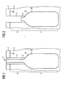
- a memory cell 1 is shown, the one Includes trench 3, which is formed in a substrate 2.
- substrate 2 consists of silicon, which can be doped with boron, phosphorus or arsenic.
- the Trench 3 has a lower area 4 and an upper area 6 on.
- the insulation collar 8 is made usually made of silicon oxide.
- a first mask 5, which acts as an etching mask for the Etching of the trench 3 is used.
- the etching mask 5 is, for example formed from silicon nitride.
- the lower area 4 of the Trench 3 which in this case is bottle-shaped is formed is a capacitor dielectric on the trench wall arranged.
- trench capacitors made of silicon oxide, silicon nitride or silicon oxynitride or any combination of these materials.
- the conductive trench filling 10 consists for example of doped silicon.
- the conductive trench filling 10 serves as an inner capacitor electrode, the outer substrate 2 as an outer capacitor electrode.
- a manufacturing process for forming the one shown in Figure 1 Trench capacitor consists in depositing one first mask 5 as a hard mask on a substrate 2, the first mask 5 is usually formed from silicon nitride.
- the first mask 5 is usually formed from silicon nitride.
- a is used to produce the first mask 5 LPCVD process (low pressure chemical vapor deposition) used.
- the first mask 5 is then structured and used as an etching mask for the etching of the trench 3.
- To the trench 3 is etched with a capacitor dielectric lined which e.g. through thermal oxidation and can be formed by CVD processes.
- the insulation collar 8 in the upper region 6 of the trench 3 is formed.
- the insulation collar 8 is formed from a silicon oxide, which is usually is applied with a CVD process.
- the senior Trench filling 10 consists of in this embodiment a highly doped polysilicon and is usually also deposited in the trench 3 by a CVD process.
- the substrate 2 is nitrided, which is exposed in the upper region 6 of the trench 3 has been. This creates a nitride layer 31, which later will serve as a diffusion barrier for dopant and electrical works as a tunnel resistor.
- FIG. 4 Furthermore (Figure 4) is in the upper region 6 of the trench 3 a conductive layer 7 is formed.
- the conductive layer 7 e.g. made of a doped polysilicon, which in a Manufacturing process by a CVD process in the trench deposited planarized and then sunk is so that the fill level shown in Figure 4 is reached.
- the isolating Cover layer 9 consists, for example, of silicon oxide and can be deposited with a CVD process, planarized and be sunk in the trench.
- the nitride layer 31 becomes the top Area 6 of the trench 3 removed.
- the nitride layer remains 31 in the area covered by the conductive layer 7 and the insulating cover layer 9 is obtained.
- the nitride layer 31 can be removed, for example, with a wet chemical process using hot phosphoric acid happen.
- FIG. 6 shows a gate oxide in the upper region 6 of the trench 3 11 formed on the exposed substrate 2. This can e.g. in a thermal process step with oxygen Atmosphere.
- FIG. 7 is a gate electrode 12 in the upper region 6 of the trench 3 is formed.
- a gate electrode 12 in the upper region 6 of the trench 3 is formed.
- CVD deposition of doped polysilicon be performed.
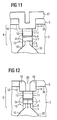
- the mask 5 is in an etching process widened so that the widening 13 above the trench 3 and arises above the substrate 2 in the first mask 5. Since the mask 5 is made of nitride, for example, the Expansion with an etching process using phosphoric acid or HFEG (HF: hydrofluoric acid, EG: ethylene glycol), which both Silicon oxide as well as silicon nitride with approximately the same Etching rates are etched.
- phosphoric acid or HFEG HF: hydrofluoric acid
- EG ethylene glycol
- a sinking process step is carried out in connection with FIG performed, the expansion 13 in the substrate and the Trench transmits, the depression 14 is formed.
- the sinking 14 can, for example, with an anisotropic etching process be performed.
- Doping region 16 A lower doping region 15 and an upper one are shown in FIG Doping region 16 is formed.
- the lower doping region 15 is created thereby by diffusion of dopant from the highly doped conductive layer 7.
- the lower doping region 15 becomes later as the lower source-drain region of the vertical transistor used.
- the upper doping region 16 is, for example formed by means of gas phase doping.
- Dopant into the substrate 2 and forms the upper doping region 16.
- the lower doping region 15 is diffused out, which is usually carried out with a temperature step the upper doping region 16 can also diffuse out, where possible crystal dislocations caused by the doping can be healed.
- the temperature step can be carried out oxidizing.
- a dielectric layer 17 is applied deposited the substrate and in the depression 14.
- the dielectric Layer 17 consists, for example, of silicon nitride and can be formed using a CVD process.
- FIG. 18 An anisotropic etching step is used in connection with FIG carried out, wherein the lateral edge webs 18 are formed (Spacer formation).
- the side ridges are in arranged the depression 14 and have an annular Structure that resembles a torus.
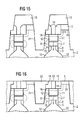
- FIG. 13 shows two adjacent memory cells.
- a second mask 19 is arranged on the substrate and been structured.
- the mask 19 is, for example from a photoresist.
- the first mask 5 with the help of second mask 19 structured.
- a anisotropic etching step used. Since the first mask 5 and the lateral edge webs 18 are made of silicon nitride both the first mask 5 and the part of the side Edge web 18 removed. A occurs in this etching process exposed area 20, which releases the substrate surface 36.
- Figure 15 the isolation trench 21 in the exposed area 20 etched into the substrate 2. It serves the first mask 5, the second mask 19 and the side mask Edge web 18 as an etching mask.
- the etching can be done with substances and Processes are performed that etch silicon while doing so proceed selectively with silicon nitride and photoresist.
- the photoresist is removed and then the side wall of the isolation trench 21 is oxidized and the isolation trench 21 is filled with an isolation trench 22 filled.
- an HDP process high density plasma CVD
- the HDP process becomes a silicon oxide as insulation trench filling 22 filled in the isolation trench 21.
- the Substrate surface 36 with a CMP process chemical mechanical polishing planarized.
- the first mask 5 and a part the side edge webs 18 removed. Since the first mask 5 and the lateral edge webs 18 are made of silicon nitride, they can be etched with hot phosphoric acid. Doing so the substrate surface 36 is exposed. Then a Scatter oxide arranged on the exposed substrate surface 36 and performed a dopant implantation, wherein the Bit line doping region 24 is formed in the substrate 2. The scatter oxide is then removed again.
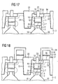
- bit line 25 is on the bit line doping area 24 formed.
- the bit line 25 consists in this Exemplary embodiment from a lower bit line layer 27 and an upper bit line layer 28.
- the lower bit line layer consists, for example, of a highly doped Polysilicon, which becomes the upper bit line layer 28 for example made of tungsten, which is less Has sheet resistance than the doped polysilicon, so that the bit line is designed to have a lower overall resistance.
- the insulation sleeve 26 is, for example made of silicon nitride.
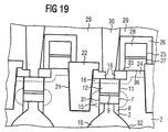
- An insulation layer 29 is then applied (FIG. 19) arranged the substrate.
- the insulation layer 29 covers thereby the bit line 25 and planarizes the surface.
- the Insulation layer 29 consists for example of a highly doped Silicate glass (BPSG) and is in one temperature step passed.
- a trench is made in the insulation layer 29 etched in which a word line contact 30 is arranged becomes.
- the word line contact 30 extends from one Word line through the insulation layer 29 and through the lateral edge webs 18 up to the gate electrode 12.
Landscapes
- Engineering & Computer Science (AREA)
- Manufacturing & Machinery (AREA)
- Semiconductor Memories (AREA)
Abstract
Description
- einem Substrat;
- einem Graben, der einen unteren Bereich, einen oberen Bereich und eine Grabenöffnung aufweist und in dem Substrat angeordnet ist;
- einem Grabenkondensator, der in dem Graben gebildet ist;
- einer leitenden Grabenfüllung, die als Bestandteil des Grabenkondensators in dem unteren Bereich des Grabens angeordnet ist;
- einem vertikalen Auswahltransistor, der in dem oberen Bereich des Grabens angeordnet ist und ein unteres Dotiergebiet, ein oberes Dotiergebiet und eine Gate-Elektrode umfaßt, wobei
- das untere Dotiergebiet im oberen Bereich des Grabens neben dem Graben in dem Substrat angeordnet ist,
- das obere Dotiergebiet im oberen Bereich des Grabens in dem Substrat, oberhalb des unteren Dotiergebietes angeordnet ist und
- die dielektrische Schicht oberhalb des Grabens angeordnet ist und eine Innenöffnung aufweist,
- wobei sich die Innenöffnung vollständig durch die dielektrische Schicht erstreckt und die dielektrische Schicht seitlich über die Grabenöffnung hinausragt.
- Bilden eines Grabens in einem Substrat, wobei eine erste Maske zur Ätzung des Grabens auf dem Substrat gebildet wird;
- Bilden eines Grabenkondensators in dem Graben;
- Bilden eines vertikalen Auswahltransistors mit einer Gate-Elektrode in dem Graben;
- Aufweiten der ersten Maske, so daß eine Aufweitung mit einem größeren Querschnitt als dem Querschnitt des Grabens freigelegt wird;
- Einsenken des Substrats und der in dem Graben angeordneten Gate-Elektrode in dem von der Aufweitung freigelegten Bereich, wobei eine Einsenkung gebildet wird;
- Bilden einer dielektrischen Schicht in der Einsenkung.
- Figur 1
- einen Grabenkondensator, der als Ausgangsbasis für das erfindungsgemäße Verfahren herangezogen wird;
- Figur 2
- einen Grabenkondensator, der aus dem in Figur 1 dargestellten Grabenkondensator durch einen Einsenkprozeß hervorgeht;
- Figur 3 bis 12
- den oberen Bereich des Grabenkondensators aus Figur 1 mit jeweils aufeinander folgenden Herstellungsschritten zur Bildung einer erfindungsgemäßen Speicherzelle;
- Figur 13 bis 19
- zwei benachbarte Speicherzellen, die sich in ihrer Herstellung an die in Figur 12 dargestellte Speicherzelle anschließen, wobei jeweils aufeinander folgende Herstellungsschritte dargestellt sind.
Claims (11)
- Speicherzelle mit:dadurch gekennzeichnet, daßeinem Substrat (2);einem Graben (3), der einen unteren Bereich (4), einen oberen Bereich (6) und eine Grabenöffnung (34) aufweist und in dem Substrat (2) angeordnet ist;einem Grabenkondensator (32), der in dem Graben (3) gebildet ist;einer leitenden Grabenfüllung (10), die als Bestandteil des Grabenkondensators (32) in dem unteren Bereich (4) des Grabens (3) angeordnet ist;einem vertikalen Auswahltransistor, der in dem oberen Bereich (6) des Grabens (3) angeordnet ist und ein unteres Dotiergebiet (15), ein oberes Dotiergebiet (16) und eine Gate-Elektrode (12) umfaßt, wobeidas untere Dotiergebiet (15) im oberen Bereich (6) des Grabens (3) neben dem Graben (3) in dem Substrat (2) angeordnet ist,das obere Dotiergebiet (16) im oberen Bereich (6) des Grabens (3) in dem Substrat (2), oberhalb des unteren Dotiergebietes (15) angeordnet ist unddie dielektrische Schicht (17, 18) oberhalb des Grabens (3) angeordnet ist und eine Innenöffnung (33) aufweist,
sich die Innenöffnung (33) vollständig durch die dielektrische Schicht (17, 18) erstreckt und die dielektrische Schicht (17, 18) seitlich über die Grabenöffnung (34) hinausragt. - Speicherzelle nach Anspruch 1,
dadurch gekennzeichnet, daß
die dielektrische Schicht (17) in das Substrat (2) eingesenkt ist. - Speicherzelle nach Anspruch 2,
dadurch gekennzeichnet, daß
die dielektrische Schicht (17) eine Oberkante (35) aufweist und das Substrat (2) eine Substratoberfläche (36) aufweist, und daß die Oberkante der dielektrischen Schicht (17) mit der Substratoberfläche (36) auf gleicher Höhe angeordnet ist. - Speicherzelle nach einem der Ansprüche 1 bis 3,
dadurch gekennzeichnet, daß
ein Isolationsgraben (21) an die dielektrischen Schicht (17) angrenzt, der mit einer Isolationsgrabenfüllung (22) gefüllt ist. - Speicherzelle nach einem der Ansprüche 1 bis 4,
dadurch gekennzeichnet, daß ein dotiertes Gebiet (24) in dem Substrat (2) angeordnet ist und an die dielektrischen Schicht (17) angrenzt. - Speicherzelle nach einem der Ansprüche 1 bis 5,
dadurch gekennzeichnet, daß
unterhalb der dielektrischen Schicht (17) eine Gate-Elektrode (12) angeordnet ist. - Verfahren zur Herstellung einer Speicherzelle mit den Schritten:Bilden eines Grabens (3) in einem Substrat (2), wobei eine erste Maske (5) zur Ätzung des Grabens (3) auf dem Substrat (2) gebildet wird;Bilden eines Grabenkondensators (32) in dem Graben (3);Bilden eines vertikalen Auswahltransistors mit einer Gate-Elektrode (12) in dem Graben (3);Aufweiten der ersten Maske (5), so daß eine Aufweitung (13) mit einem größeren Querschnitt als dem Querschnitt des Grabens (3) freigelegt wird;Einsenken des Substrats (2) und der in dem Graben (3) angeordneten Gate-Elektrode (12) in dem von der Aufweitung (13) freigelegten Bereich, wobei eine Einsenkung (14) gebildet wird;Bilden einer dielektrischen Schicht (17, 18) in der Einsenkung (14).
- Verfahren nach Anspruch 7,
dadurch gekennzeichnet, daß
Dotierstoff in dem Bereich der Einsenkung (14) in das Substrat (2) eingebracht wird und ein oberes Dotiergebiet (16) bildet. - Verfahren nach einem der Ansprüche 7 oder 8,
dadurch gekennzeichnet, daß
eine dielektrische Schicht (17) in der Einsenkung (14) abgeschieden wird und mit einem anisotropen Ätzprozeß seitliche Randstege (18) aus der dielektrischen Schicht (17) gebildet werden. - Verfahren nach einem der Ansprüche 7 bis 9,
dadurch gekennzeichnet, daß
eine zweite Maske (19) auf dem Substrat (2) angeordnet und strukturiert wird, und daß das Substrat in einem Bereich (20), der zwischen benachbarten Grabenkondensatoren liegt, freigelegt wird. - Verfahren nach Anspruch 10,
dadurch gekennzeichnet, daß
die erste Maske (5), die zweite Maske (19) und die seitlichen Randstege (18) eine gemeinsame Ätzmaske beim Ätzen eines Isolationsgrabens (21) bilden.
Applications Claiming Priority (2)
| Application Number | Priority Date | Filing Date | Title |
|---|---|---|---|
| DE10027913 | 2000-05-31 | ||
| DE10027913A DE10027913A1 (de) | 2000-05-31 | 2000-05-31 | Speicherzelle mit einem Grabenkondensator |
Publications (2)
| Publication Number | Publication Date |
|---|---|
| EP1160855A2 true EP1160855A2 (de) | 2001-12-05 |
| EP1160855A3 EP1160855A3 (de) | 2006-06-28 |
Family
ID=7644818
Family Applications (1)
| Application Number | Title | Priority Date | Filing Date |
|---|---|---|---|
| EP01110456A Withdrawn EP1160855A3 (de) | 2000-05-31 | 2001-04-27 | Speicherzelle mit einem Grabenkondensator und Verfahren zu ihrer Herstellung |
Country Status (6)
| Country | Link |
|---|---|
| US (1) | US6420239B2 (de) |
| EP (1) | EP1160855A3 (de) |
| JP (1) | JP3648463B2 (de) |
| KR (1) | KR100419926B1 (de) |
| DE (1) | DE10027913A1 (de) |
| TW (1) | TW515049B (de) |
Cited By (2)
| Publication number | Priority date | Publication date | Assignee | Title |
|---|---|---|---|---|
| WO2002049100A3 (en) * | 2000-12-14 | 2003-04-03 | Infineon Technologies Corp | Method of forming vertical transistor gate for trench capacitor dram cell |
| EP1553631A2 (de) | 2004-01-09 | 2005-07-13 | International Business Machines Corporation | Nitridierte STI-Oxidtrennschicht zum reduzierten Einfluss von Ecken auf die Leistung von vertikalen Vorrichtungen |
Families Citing this family (10)
| Publication number | Priority date | Publication date | Assignee | Title |
|---|---|---|---|---|
| DE10113187C1 (de) * | 2001-03-19 | 2002-08-29 | Infineon Technologies Ag | Verfahren zur Herstellung eines Grabenkondensators einer Speicherzelle eines Halbleiterspeichers |
| US6552382B1 (en) * | 2002-09-30 | 2003-04-22 | Intelligent Sources Development Corp. | Scalable vertical DRAM cell structure and its manufacturing methods |
| US6660581B1 (en) * | 2003-03-11 | 2003-12-09 | International Business Machines Corporation | Method of forming single bitline contact using line shape masks for vertical transistors in DRAM/e-DRAM devices |
| US20050285175A1 (en) * | 2004-06-23 | 2005-12-29 | International Business Machines Corporation | Vertical SOI Device |
| US7078756B2 (en) * | 2004-12-06 | 2006-07-18 | International Business Machines Corporation | Collarless trench DRAM device |
| US7371645B2 (en) * | 2005-12-30 | 2008-05-13 | Infineon Technologies Ag | Method of manufacturing a field effect transistor device with recessed channel and corner gate device |
| KR100733703B1 (ko) * | 2006-08-29 | 2007-06-28 | 동부일렉트로닉스 주식회사 | 반도체 소자 및 이의 제조 방법 |
| KR20100040455A (ko) * | 2008-10-10 | 2010-04-20 | 주식회사 동부하이텍 | 반도체 소자의 제조 방법 |
| FR3021524A1 (fr) | 2014-06-02 | 2015-12-04 | Small Bone Innovations Internat | Tige d'ancrage metacarpien, notamment pour une prothese trapezo-metacarpienne |
| US11171200B2 (en) * | 2019-09-26 | 2021-11-09 | Texas Instruments Incorporated | Integrated circuits having dielectric layers including an anti-reflective coating |
Family Cites Families (31)
| Publication number | Priority date | Publication date | Assignee | Title |
|---|---|---|---|---|
| US302204A (en) * | 1884-07-15 | bibby | ||
| DE905771C (de) * | 1941-11-18 | 1954-03-04 | Huettenwerk Huckingen A G | Verfahren zur Herstellung eines Grundiermittels aus Steinkohlenteerpech und organischen Loesungsmitteln |
| DE852396C (de) * | 1951-06-02 | 1952-10-13 | Gussstahlwerk Bochumer Ver Ag | Ausbildung der Zungenvorrichtung von Weichen fuer rueckbare Gleise |
| DE884785C (de) * | 1952-01-23 | 1953-07-30 | Albert Glemser | Durch Anschluss an die Wasserleitung betriebene Kolben-Waeschepresse |
| US4672410A (en) * | 1984-07-12 | 1987-06-09 | Nippon Telegraph & Telephone | Semiconductor memory device with trench surrounding each memory cell |
| US5208657A (en) | 1984-08-31 | 1993-05-04 | Texas Instruments Incorporated | DRAM Cell with trench capacitor and vertical channel in substrate |
| US4864375A (en) * | 1986-02-05 | 1989-09-05 | Texas Instruments Incorporated | Dram cell and method |
| US4816884A (en) * | 1987-07-20 | 1989-03-28 | International Business Machines Corporation | High density vertical trench transistor and capacitor memory cell structure and fabrication method therefor |
| US5183774A (en) * | 1987-11-17 | 1993-02-02 | Mitsubishi Denki Kabushiki Kaisha | Method of making a semiconductor memory device |
| JPH01171266A (ja) * | 1987-12-25 | 1989-07-06 | Matsushita Electric Ind Co Ltd | 半導体メモリ装置 |
| US4958212A (en) * | 1988-12-30 | 1990-09-18 | Texas Instruments Incorporated | Trench memory cell |
| US5162250A (en) * | 1989-06-30 | 1992-11-10 | Texas Instruments, Incorporated | Method for interconnecting a filament channel transistor with a wordline conductor |
| JPH0414868A (ja) | 1990-05-09 | 1992-01-20 | Hitachi Ltd | 半導体記憶装置とその製造方法 |
| KR940006679B1 (ko) * | 1991-09-26 | 1994-07-25 | 현대전자산업 주식회사 | 수직형 트랜지스터를 갖는 dram셀 및 그 제조방법 |
| US5641694A (en) * | 1994-12-22 | 1997-06-24 | International Business Machines Corporation | Method of fabricating vertical epitaxial SOI transistor |
| US6207494B1 (en) * | 1994-12-29 | 2001-03-27 | Infineon Technologies Corporation | Isolation collar nitride liner for DRAM process improvement |
| US5576566A (en) * | 1995-04-13 | 1996-11-19 | International Business Machines Corporation | Semiconductor trench capacitor cell having a buried strap |
| US5937296A (en) * | 1996-12-20 | 1999-08-10 | Siemens Aktiengesellschaft | Memory cell that includes a vertical transistor and a trench capacitor |
| US5915175A (en) * | 1997-06-27 | 1999-06-22 | Siemens Aktiengesellschaft | Mitigation of CMP-induced BPSG surface damage by an integrated anneal and silicon dioxide deposition |
| US5831301A (en) * | 1998-01-28 | 1998-11-03 | International Business Machines Corp. | Trench storage dram cell including a step transfer device |
| US6225158B1 (en) * | 1998-05-28 | 2001-05-01 | International Business Machines Corporation | Trench storage dynamic random access memory cell with vertical transfer device |
| TW385542B (en) * | 1998-07-31 | 2000-03-21 | Siemens Ag | Method for making deep trench capacitor by two stage ion implantment |
| DE19844997A1 (de) * | 1998-09-30 | 2000-04-13 | Siemens Ag | Vertikaler Feldeffekttransistor mit innenliegendem Gate und Herstellverfahren |
| US6140175A (en) * | 1999-03-03 | 2000-10-31 | International Business Machines Corporation | Self-aligned deep trench DRAM array device |
| TW439267B (en) * | 1999-11-29 | 2001-06-07 | Winbond Electronics Corp | Fabricating method of bottom electrode for buried type capacitor |
| US6150670A (en) * | 1999-11-30 | 2000-11-21 | International Business Machines Corporation | Process for fabricating a uniform gate oxide of a vertical transistor |
| TW426947B (en) * | 1999-12-09 | 2001-03-21 | Mosel Vitelic Inc | Method of producing trench capacitor |
| DE10011889A1 (de) * | 2000-03-07 | 2001-09-20 | Infineon Technologies Ag | Speicherzelle mit Graben und Verfahren zu ihrer Herstellung |
| DE10024876A1 (de) * | 2000-05-16 | 2001-11-29 | Infineon Technologies Ag | Vertikaler Transistor |
| US6309924B1 (en) * | 2000-06-02 | 2001-10-30 | International Business Machines Corporation | Method of forming self-limiting polysilicon LOCOS for DRAM cell |
| TW466684B (en) * | 2000-09-29 | 2001-12-01 | United Microelectronics Corp | Method for forming deep trench capacitor under shallow trench isolation structure |
-
2000
- 2000-05-31 DE DE10027913A patent/DE10027913A1/de not_active Ceased
-
2001
- 2001-04-27 EP EP01110456A patent/EP1160855A3/de not_active Withdrawn
- 2001-05-28 JP JP2001159367A patent/JP3648463B2/ja not_active Expired - Fee Related
- 2001-05-29 TW TW090112880A patent/TW515049B/zh not_active IP Right Cessation
- 2001-05-31 US US09/871,010 patent/US6420239B2/en not_active Expired - Fee Related
- 2001-05-31 KR KR10-2001-0030336A patent/KR100419926B1/ko not_active Expired - Fee Related
Cited By (3)
| Publication number | Priority date | Publication date | Assignee | Title |
|---|---|---|---|---|
| WO2002049100A3 (en) * | 2000-12-14 | 2003-04-03 | Infineon Technologies Corp | Method of forming vertical transistor gate for trench capacitor dram cell |
| EP1553631A2 (de) | 2004-01-09 | 2005-07-13 | International Business Machines Corporation | Nitridierte STI-Oxidtrennschicht zum reduzierten Einfluss von Ecken auf die Leistung von vertikalen Vorrichtungen |
| EP1553631A3 (de) * | 2004-01-09 | 2009-10-07 | International Business Machines Corporation | Nitridierte STI-Oxidtrennschicht zum reduzierten Einfluss von Ecken auf die Leistung von vertikalen Vorrichtungen |
Also Published As
| Publication number | Publication date |
|---|---|
| KR20010109198A (ko) | 2001-12-08 |
| TW515049B (en) | 2002-12-21 |
| DE10027913A1 (de) | 2001-12-13 |
| US20020004271A1 (en) | 2002-01-10 |
| JP3648463B2 (ja) | 2005-05-18 |
| JP2002016148A (ja) | 2002-01-18 |
| EP1160855A3 (de) | 2006-06-28 |
| KR100419926B1 (ko) | 2004-02-25 |
| US6420239B2 (en) | 2002-07-16 |
Similar Documents
| Publication | Publication Date | Title |
|---|---|---|
| DE19941148B4 (de) | Speicher mit Grabenkondensator und Auswahltransistor und Verfahren zu seiner Herstellung | |
| EP1364373B1 (de) | Verfahren zur herstellung eines speicherkondensators | |
| DE19944012B4 (de) | Grabenkondensator mit Kondensatorelektroden und entsprechendes Herstellungsverfahren | |
| EP1182699B1 (de) | Verfahren zur Bildung eines dicken dielektrischen Gebietes in einem Halbleitersubstrat | |
| DE102006049158A1 (de) | Transistor, Speicherzellenfeld und Verfahren zur Herstellung eines Transistors | |
| DE10019090A1 (de) | Grabenkondensator sowie dazugehöriges Herstellungsverfahren | |
| DE10014920C1 (de) | Verfahren zur Herstellung eines Grabenkondensators | |
| DE102005054431A1 (de) | Verfahren zum Herstellen eines Flaschengrabens und eines Flaschengrabenkondensators | |
| EP0875937A2 (de) | DRAM-Zellenanordnung und Verfahren zu deren Herstellung | |
| DE10111755C1 (de) | Verfahren zur Herstellung einer Speicherzelle eines Halbleiterspeichers | |
| DE102006038532A1 (de) | Halbleiter-Speicherzellenfeld mit selbstjustierenden rückgeätzten Gate-MOS-Transistoren und Verfahren zu dessen Herstellung | |
| EP1160855A2 (de) | Speicherzelle mit einem Grabenkondensator und Verfahren zu ihrer Herstellung | |
| DE19911148C1 (de) | DRAM-Zellenanordnung und Verfahren zu deren Herstellung | |
| DE10120053A1 (de) | Stressreduziertes Schichtsystem | |
| WO1997044826A1 (de) | Dram-zellenanordnung und verfahren zu deren herstellung | |
| EP0945901A1 (de) | DRAM-Zellenanordnung mit vertikalen Transistoren und Verfahren zu deren Herstellung | |
| EP1540725B1 (de) | Verfahren zur herstellung eines halbleiterbauteils mit im substrat vergrabenen kondensatoren und davon isolierter bauelementschicht | |
| DE19946719A1 (de) | Grabenkondensator und Verfahren zu seiner Herstellung | |
| EP1145320A1 (de) | Dram-zellenanordnung und verfahren zur deren herstellung | |
| WO2000019528A9 (de) | Dram-zellenanordnung und verfahren zu deren herstellung | |
| WO2002069375A2 (de) | Grabenkondensator und verfahren zu seiner herstellung | |
| DE102004007242A1 (de) | Grabenkondensator mit vergrabener Kontaktbrücke | |
| DE10111760B4 (de) | Verfahren zur Herstellung von mindestens zwei Speicherzellen eines Halbleiterspeichers | |
| EP0925607B1 (de) | Verfahren zur herstellung einer dram-zellenanordnung | |
| DE19914490C1 (de) | Speicherzellenanordnung und Verfahren zu deren Herstellung |
Legal Events
| Date | Code | Title | Description |
|---|---|---|---|
| PUAI | Public reference made under article 153(3) epc to a published international application that has entered the european phase |
Free format text: ORIGINAL CODE: 0009012 |
|
| AK | Designated contracting states |
Kind code of ref document: A2 Designated state(s): AT BE CH CY DE DK ES FI FR GB GR IE IT LI LU MC NL PT SE TR |
|
| AX | Request for extension of the european patent |
Free format text: AL;LT;LV;MK;RO;SI |
|
| PUAL | Search report despatched |
Free format text: ORIGINAL CODE: 0009013 |
|
| AK | Designated contracting states |
Kind code of ref document: A3 Designated state(s): AT BE CH CY DE DK ES FI FR GB GR IE IT LI LU MC NL PT SE TR |
|
| AX | Request for extension of the european patent |
Extension state: AL LT LV MK RO SI |
|
| AKX | Designation fees paid | ||
| STAA | Information on the status of an ep patent application or granted ep patent |
Free format text: STATUS: THE APPLICATION IS DEEMED TO BE WITHDRAWN |
|
| 18D | Application deemed to be withdrawn |
Effective date: 20061229 |
|
| REG | Reference to a national code |
Ref country code: DE Ref legal event code: 8566 |