EP1146590A2 - Oberflächenmontierte Antenne und Funkgerät mit einer derartigen Antenne - Google Patents
Oberflächenmontierte Antenne und Funkgerät mit einer derartigen Antenne Download PDFInfo
- Publication number
- EP1146590A2 EP1146590A2 EP01107520A EP01107520A EP1146590A2 EP 1146590 A2 EP1146590 A2 EP 1146590A2 EP 01107520 A EP01107520 A EP 01107520A EP 01107520 A EP01107520 A EP 01107520A EP 1146590 A2 EP1146590 A2 EP 1146590A2
- Authority
- EP
- European Patent Office
- Prior art keywords
- feeding
- mounted antenna
- radiation
- resonance
- wave
- Prior art date
- Legal status (The legal status is an assumption and is not a legal conclusion. Google has not performed a legal analysis and makes no representation as to the accuracy of the status listed.)
- Granted
Links
Images


Classifications
-
- H—ELECTRICITY
- H01—ELECTRIC ELEMENTS
- H01Q—ANTENNAS, i.e. RADIO AERIALS
- H01Q5/00—Arrangements for simultaneous operation of antennas on two or more different wavebands, e.g. dual-band or multi-band arrangements
-
- H—ELECTRICITY
- H01—ELECTRIC ELEMENTS
- H01Q—ANTENNAS, i.e. RADIO AERIALS
- H01Q1/00—Details of, or arrangements associated with, antennas
- H01Q1/12—Supports; Mounting means
- H01Q1/22—Supports; Mounting means by structural association with other equipment or articles
- H01Q1/24—Supports; Mounting means by structural association with other equipment or articles with receiving set
- H01Q1/241—Supports; Mounting means by structural association with other equipment or articles with receiving set used in mobile communications, e.g. GSM
- H01Q1/242—Supports; Mounting means by structural association with other equipment or articles with receiving set used in mobile communications, e.g. GSM specially adapted for hand-held use
- H01Q1/243—Supports; Mounting means by structural association with other equipment or articles with receiving set used in mobile communications, e.g. GSM specially adapted for hand-held use with built-in antennas
-
- H—ELECTRICITY
- H01—ELECTRIC ELEMENTS
- H01Q—ANTENNAS, i.e. RADIO AERIALS
- H01Q1/00—Details of, or arrangements associated with, antennas
- H01Q1/36—Structural form of radiating elements, e.g. cone, spiral, umbrella; Particular materials used therewith
- H01Q1/38—Structural form of radiating elements, e.g. cone, spiral, umbrella; Particular materials used therewith formed by a conductive layer on an insulating support
-
- H—ELECTRICITY
- H01—ELECTRIC ELEMENTS
- H01Q—ANTENNAS, i.e. RADIO AERIALS
- H01Q19/00—Combinations of primary active antenna elements and units with secondary devices, e.g. with quasi-optical devices, for giving the antenna a desired directional characteristic
- H01Q19/005—Patch antenna using one or more coplanar parasitic elements
-
- H—ELECTRICITY
- H01—ELECTRIC ELEMENTS
- H01Q—ANTENNAS, i.e. RADIO AERIALS
- H01Q5/00—Arrangements for simultaneous operation of antennas on two or more different wavebands, e.g. dual-band or multi-band arrangements
- H01Q5/30—Arrangements for providing operation on different wavebands
- H01Q5/307—Individual or coupled radiating elements, each element being fed in an unspecified way
- H01Q5/314—Individual or coupled radiating elements, each element being fed in an unspecified way using frequency dependent circuits or components, e.g. trap circuits or capacitors
- H01Q5/321—Individual or coupled radiating elements, each element being fed in an unspecified way using frequency dependent circuits or components, e.g. trap circuits or capacitors within a radiating element or between connected radiating elements
-
- H—ELECTRICITY
- H01—ELECTRIC ELEMENTS
- H01Q—ANTENNAS, i.e. RADIO AERIALS
- H01Q5/00—Arrangements for simultaneous operation of antennas on two or more different wavebands, e.g. dual-band or multi-band arrangements
- H01Q5/30—Arrangements for providing operation on different wavebands
- H01Q5/307—Individual or coupled radiating elements, each element being fed in an unspecified way
- H01Q5/342—Individual or coupled radiating elements, each element being fed in an unspecified way for different propagation modes
- H01Q5/357—Individual or coupled radiating elements, each element being fed in an unspecified way for different propagation modes using a single feed point
- H01Q5/364—Creating multiple current paths
- H01Q5/371—Branching current paths
-
- H—ELECTRICITY
- H01—ELECTRIC ELEMENTS
- H01Q—ANTENNAS, i.e. RADIO AERIALS
- H01Q5/00—Arrangements for simultaneous operation of antennas on two or more different wavebands, e.g. dual-band or multi-band arrangements
- H01Q5/30—Arrangements for providing operation on different wavebands
- H01Q5/378—Combination of fed elements with parasitic elements
-
- H—ELECTRICITY
- H01—ELECTRIC ELEMENTS
- H01Q—ANTENNAS, i.e. RADIO AERIALS
- H01Q9/00—Electrically-short antennas having dimensions not more than twice the operating wavelength and consisting of conductive active radiating elements
- H01Q9/04—Resonant antennas
- H01Q9/0407—Substantially flat resonant element parallel to ground plane, e.g. patch antenna
- H01Q9/0414—Substantially flat resonant element parallel to ground plane, e.g. patch antenna in a stacked or folded configuration
Definitions
- the present invention relates to surface-mounted antennas capable of transmitting and receiving the signals of different frequency bands and wireless devices incorporating the same.
- GSM global system for mobile communications
- DCS digital cellular system
- PDC personal digital cellular
- PHS personal handyphone system
- various antennas In these cases, the signals of different frequency bands can be transmitted and received by using only a single antenna.
- Such an antenna has many problems in handling multi-bands. Particularly, in required multiple frequency bands, in a region closer to the high-frequency side, the frequency bandwidth tends to be narrower. As a result, it is difficult to obtain bandwidths allocated to the applications. In addition, it is extremely difficult to control the frequency bandwidths independently from each other. These are critical problems to be solved.
- the signals of different frequency bands can be transmitted and received by the single antenna. Additionally, the broadening of frequency bands can be easily made, and particularly, the frequency bandwidths can be controlled independently from each other. Furthermore, it is another object of the invention to provide a wireless device incorporating the multi-band surface-mounted antenna.
- a surface-mounted antenna including a dielectric base member, a feeding element formed by extending a radiation electrode from a feeding terminal on the dielectric base member, and a non-feeding element formed by extending a radiation electrode from a ground terminal on the dielectric base member.
- the feeding element and the non-feeding element are arranged via a distance therebetween.
- at least one of the feeding element and the non-feeding element is a branched element formed by extending a plurality of radiation electrodes branched from the feeding-terminal side or the ground-terminal side via a distance therebetween.
- the plurality of radiation electrodes forming the branched element may have different fundamental-wave resonance frequencies.
- the plurality of radiation electrodes forming the branched element may be extended from one of the feeding-terminal side and the ground-terminal side in directions in which the distance between the radiation electrodes is expanded.
- At least one of the plurality of radiation electrodes forming the feeding element and the non-feeding element may locally include at least one of a fundamental-wave controlling unit for controlling a fundamental-wave resonance frequency and a harmonic controlling unit for controlling a harmonic resonance frequency.
- the fundamental wave controlling unit may be locally disposed in a fundamental-wave maximum resonance current region including a maximum current portion at which a fundamental-wave resonance current reaches a maximum on a current path of the radiation electrode.
- the harmonic controlling unit may be locally disposed in a harmonic maximum resonance current region including a maximum current portion at which a harmonic resonance current reaches a maximum on the current path of the radiation electrode.
- the feeding element there may be alternately arranged a region of a small current length per unit length and a region of a large current length per unit length along the current path.
- At least one of the branched radiation electrodes of one of the feeding element and the non-feeding element may perform combined resonance with a radiation electrode of the remaining element.
- electric power may be supplied to the feeding terminal of the feeding element by capacitive coupling.
- a wireless device including the surface-mounted antenna described above.
- the resonance wave having the lowest resonance frequency is defined as the fundamental wave
- the resonance waves having resonance frequencies higher than that of the fundamental wave are defined as the harmonics.
- a state in which there are two or more resonance points within one frequency band is defined as combined resonance.
- the three radiation electrodes are formed on a surface of the dielectric base member so that the antenna is easily adaptable to multi-bands. Moreover, by setting the current-vector directions of the radiation electrodes and the distances between the radiation electrodes according to needs, the resonance waves of the radiation electrodes can be controlled independently from each other. Thus, for example, only one frequency band of required frequency bands is selected to set in a multi-resonance state so that broadening of the used frequency band can be very easily achieved.
- Fig. 1 shows a developed view of a surface-mounted antenna according to a first embodiment of the invention.
- a surface-mounted antenna 1 shown in Fig. 1 on a rectangular-parallelepiped dielectric base member 2, a feeding element 3 and a non-feeding element 4 are arranged with a distance therebetween.
- the non-feeding element 4 is formed as a branched element.
- a radiation electrode 7 of the feeding side is formed on an upper surface 2a of the dielectric base member 2.
- the radiation electrode 7 of the feeding side is extended from the upper surface 2a to a left side surface 2e in the figure.
- a top end 7b of the extended radiation electrode 7 of the feeding side is open-circuited.
- a first radiation electrode 8 and a second radiation electrode 9 of the non-feeding side having meandering shapes branched and extended from the ground terminal 6 are arranged with a distance between the electrodes 8 and 9.
- the feeding element 3 is formed by the feeding terminal 5 and the feeding-side radiation electrode 7.
- the non-feeding element 4 is formed by the ground terminal 6 and the non-feeding-side first and second radiation electrodes 8 and 9. As mentioned above, the non-feeding element 4 is formed as a branched element.
- the non-feeding-side first and second radiation electrodes 8 and 9, as shown in Fig. 1, are extended from the ground terminal 6 in directions in which the distance therebetween is expanded. With this arrangement, the mutual interference between the non-feeding-side first and second radiation electrodes 8 and 9 is prevented. A top end 8b of the extended non-feeding-side first radiation electrode 8 is open-circuited.
- the non-feeding-side second radiation electrode 9 is extended to a right side surface 2c from the upper surface 2a in the figure. A top end 9b of the extended non-feeding-side second radiation electrode 9 is open-circuited.
- the directions of the current vectors of the electrodes 7 and 8 are substantially orthogonal to each other. With this arrangement, the mutual interference between the feeding-side radiation electrode 7 and the non-feeding-side first radiation electrode 8 is prevented.
- the directions of the current vectors of the feeding-side radiation electrode 7 and the non-feeding-side second radiation electrode 9 are almost the same. However, there is a large distance between the feeding-side radiation electrode 7 and the non-feeding-side second radiation electrode 9.
- both radiation electrodes 7 and 9 where the electric fields are the largest, are oriented to mutually opposite directions and also, there is a large distance therebetween. Thus, there is substantially no mutual interference between the feeding-side radiation electrode 7 and the non-feeding-side second radiation electrode 9.
- fixing electrodes 10 10a, 10b, 10c, and 10d, which are extended down to the bottom surface 2f.
- through-holes 11 (11a and 11b) penetrating from the front side surface 2b of the dielectric base member 2 to a backside surface 2d thereof.
- the weight of the dielectric base member 2 can be reduced.
- effective permeability between the ground and the radiation electrodes 7, 8, and 9 is reduced and electric-field concentration is lowered, with the result that a used frequency band can be broadened and a high gain can be obtained.
- the surface-mounted antenna 1 shown in Fig. 1 is mounted on a circuit board of a wireless device such as a mobile phone.
- a wireless device such as a mobile phone.
- the bottom surface 2f with respect to the upper surface 2a of the dielectric base member 2 is used as a bottom surface when mounted.
- a signal supply source 12 and a matching circuit 13 are formed on the circuit board of the wireless device.
- the feeding terminal 5 of the surface-mounted antenna 1 is electrically connected to the signal supply source 12 via the matching circuit 13.
- the matching circuit 13 is incorporated in the circuit board of the wireless device.
- a meandering electrode pattern may be formed as the matching circuit 13 on the bottom surface 2f of the dielectric base member 2.
- the signal when a signal is directly supplied to the feeding terminal 5 from the signal supply source 12 via the matching circuit 13, the signal is then supplied from the feeding terminal 5 to the feeding-side radiation electrode 7, and at the same time, by electromagnetic coupling, the signal is also supplied to the non-feeding-side first and second radiation electrodes 8 and 9.
- the feeding-side radiation electrode 7 and the non-feeding-side first and second radiation electrodes 8 and 9 With the supply of the signal, in the feeding-side radiation electrode 7 and the non-feeding-side first and second radiation electrodes 8 and 9, currents flow from base ends 7a, 8a, and 9a of the electrodes 7, 8, and 9 to the open-circuited ends 7b, 8b, and 9b thereof.
- the feeding-side radiation electrode 7 and the non-feeding-side first and second radiation electrodes 8 and 9 resonate, by which signal transmission/reception is performed.
- Fig. 3 there are shown the typical current distributions of one of the radiation electrodes indicated by dotted lines and typical voltage distributions thereof indicated by solid lines, regarding a fundamental wave, a second-order wave (harmonic), and a third-order wave (harmonic).
- the end A corresponds to the signal supplying side of each of the radiation electrodes 7, 8, and 9, that is, the base-end sides 7a, 8a, and 9a.
- the end B corresponds to the open-circuited ends 7b, 8b, and 9b thereof.
- each resonance wave has a unique current distribution and a unique voltage distribution.
- the maximum resonance current region of the fundamental wave that is, a region Z1 including a maximum current portion Imax at which the fundamental-wave resonance current reaches a maximum, lies at each of the base ends 7a, 8a, and 9a of the radiation electrodes 7, 8, and 9.
- the maximum resonance current region of the second-order harmonic that is, a region Z2 including a maximum current portion Imax at which the second-order-wave resonance current reaches a maximum, lies at each center of the radiation electrodes 7, 8, and 9.
- the maximum resonance current regions of the resonance waves of the radiation electrodes 7, 8, and 9 are positioned in the mutually different points.
- a meandering pattern 15 in the maximum resonance current region Z1 of the fundamental wave and a meandering pattern 16 in the maximum resonance current region Z2 of the second-order wave there are partially formed a meandering pattern 15 in the maximum resonance current region Z1 of the fundamental wave and a meandering pattern 16 in the maximum resonance current region Z2 of the second-order wave.
- a series inductance component is locally added to each of the maximum resonance current region Z1 of the fundamental wave and the maximum resonance current region Z2 of the second-order wave on the feeding-side radiation electrode 7.
- an electric length per unit length in each of the regions Z1 and Z2 is larger than that that in the other region.
- the region having the large electric length per unit length and the region having the small electric length per unit length are alternately arranged in series along a current path.
- a resonance frequency f1 of the fundamental wave can be controlled by changing the magnitude of the series inductance component composed of the meandering pattern 15 formed in the maximum resonance current region Z1 of the fundamental wave. In this case, there are very few influences whereby the resonance frequencies of the other resonance waves are changed.
- a resonance frequency f2 of the second-order wave (harmonic) can be changed in a state independent from the other resonance waves by changing the magnitude of the series inductance component composed of the meandering pattern 16 formed in the maximum resonance current region Z2 of the second-order wave.
- the meandering pattern 15 can serve as the fundamental-wave controlling unit for controlling the resonance frequency f1 of the fundamental wave
- the meandering pattern 16 can serve as the harmonic controlling unit for controlling the resonance frequency f2 of the second-order wave as a harmonic.
- the numbers of the meandering lines, the distance between the meandering lines, and the widths of the meandering lines, and the like may be changed. However, the explanation about these possible changes will be omitted.
- the meandering patterns 15 and 16 By partially disposing the above-mentioned meandering patterns 15 and 16 on the feeding-side radiation electrode 7, it is possible to easily design the feeding-side radiation electrode 7 in order to set the resonance frequency f1 of the fundamental wave and the resonance frequency f2 of the second-order harmonic at desired frequencies.
- the meandering pattern 15 or 16 formed in the maximum resonance current region of a resonance wave having a frequency as a target for adjustment is trimmed to change the magnitude of the series inductance component.
- the deviated frequency can coincide with the set frequency.
- the frequencies of resonance waves except the resonance wave having the frequency as the target for adjustment hardly change.
- the resonance frequency can be simply and quickly adjusted.
- the surface-mounted antenna 1 shown in the first embodiment is formed above.
- the lengths of the current paths in the radiation electrodes 7, 8, and 9 the magnitudes of the series inductance components composed of the meandering patterns 15 and 16 formed on the feeding-side radiation electrode 7, and the like, are changed in various manners, the surface-mounted antenna 1 can have various return loss characteristics.
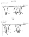
- the surface-mounted antenna 1 can have return loss characteristics as indicated by the solid lines D shown in Figs. 2A and 2B.
- the dash-single-dot lines A indicate the return loss characteristics of the feeding-side radiation electrode 7
- the dash-double-dot lines B indicate the return loss characteristics of the non-feeding-side first radiation electrode 8.
- the dotted lines C indicate the return loss characteristics of the non-feeding-side second radiation 9.
- the frequency f1 is the fundamental-wave resonance frequency of the feeding-side radiation electrode 7
- the frequency f2 is the second-order-wave resonance frequency of the feeding-side radiation electrode 7.
- the frequency f3 is the fundamental-wave resonance frequency of the non-feeding-side first radiation electrode 8
- the frequency f4 is the fundamental-wave resonance frequency of the non-feeding-side second radiation electrode 9.
- the fundamental-wave resonance frequency f1 of the feeding-side radiation electrode 7 is set in such a manner that the low frequency band of the required two frequency bands can be obtained.
- the second-order-wave resonance frequency f2 of the feeding-side radiation electrode 7 is set in such a manner that the high frequency band thereof can be obtained.
- the fundamental-wave resonance frequency f3 of the non-feeding-side first radiation electrode 8 is set above the second-order-wave resonance frequency f2 of the feeding-side radiation electrode 7, and the fundamental-wave resonance frequency f4 of the non-feeding-side second radiation electrode 9 is set below the second-order-wave resonance frequency f2 of the feeding-side radiation electrode 7.
- the fundamental-wave resonance frequency f3 of the non-feeding-side first radiation electrode 8 and the fundamental-wave resonance frequency f4 of the non-feeding-side second radiation electrode 9 are set near the second-order-wave resonance frequency f2 of the feeding-side radiation electrode 7. Additionally, as mentioned above, in the first embodiment, the mutual interference between the radiation electrodes 7, 8, and 9 can be prevented. Therefore, without problems such as attenuation of the resonance waves, the fundamental waves of the non-feeding-side first and second radiation electrodes 8 and 9 perform combined resonance (overlapping), and as shown in Fig. 2A, the frequency band of the high-frequency side can be broadened.
- the resonance frequency f1 of the fundamental wave and the resonance frequency f2 of the second-order-wave of the feeding-side radiation electrode 7 are set in the same manner as those shown in Fig. 2A. That is, the resonance frequency f4 of the fundamental wave of the non-feeding-side second radiation electrode 9 is set near the resonance frequency f1 of the fundamental wave of the feeding-side radiation electrode 7, and the fundamental wave of the non-feeding-side second radiation electrode 9 performs combined resonance with the fundamental wave of the feeding-side radiation electrode 7.
- the resonance frequency f3 of the fundamental wave of the non-feeding-side first radiation electrode 8 is set near the resonance frequency f2 of the second-order harmonic of the feeding-side radiation electrode 7, and the fundamental wave of the non-feeding-side first radiation electrode 8 performs combined resonance with the second-order harmonic of the feeding-side radiation electrode 7.
- the frequency bands of both of the low and high frequency sides are in the multi-resonance states so that broadening of the used frequency band can be achieved.
- the return loss characteristics shown in Figs. 2A and 2B are used to instantiate return loss characteristics obtainable by the surface-mounted antenna 1 according to the first embodiment.
- the radiation electrodes 7, 8, and 9 according to necessity, return loss characteristics unlike those shown in the Figs. 2A and 2B can be obtained. The explanation thereof will be omitted.
- the non-feeding element 4 is formed as a branched element composed of the two radiation electrodes 8 and 9.
- the single surface-mounted antenna 1 includes three radiation electrodes 7, 8, and 9, by which the surface-mounted antenna 1 can be easily adapted to multi-bands.
- the non-feeding-side first and second radiation electrodes 8 and 9 are extended in the directions in which the distance between the electrodes 8 and 9 is expanded from the base ends 8a and 9a thereof.
- the mutual interference between the non-feeding-side first and second radiation electrodes 8 and 9 can be prevented.
- each of the resonance waves of the non-feeding-side first and second radiation electrodes 8 and 9 can be controlled in a state substantially independent from the other. With this arrangement, the multi-band adaptability of the antenna 1 can be further enhanced.
- the meandering pattern 15 as the fundamental-wave controlling unit and the meandering pattern 16 as the harmonic controlling unit are disposed on the feeding-side radiation electrode 7.
- designing of the feeding-side radiation electrode 7 can be simplified to complete it in a short time.
- the resonance frequency f1 of the fundamental wave and the resonance frequency f2 of the harmonic can be easily adjusted, with the result that the surface-mounted antenna 1 can have highly reliable antenna characteristics.
- the resonance waves of the non-feeding-side first and second radiation electrodes 8 and 9 can simply perform multi-resonance with the fundamental wave and the harmonic of the feeding-side radiation electrode 7.
- the used frequency band can be broadened.
- the multi-band surface-mounted antenna 1 can be designed easily.
- Fig. 4 shows a developed view of a surface-mounted antenna according to the second embodiment of the invention.
- a surface-mounted antenna 1 shown in the second embodiment has a structure different from that of the first embodiment.
- both a non-feeding element 4 and a feeding element 3 are branched elements.
- feeding-side first and second radiation electrodes 20 and 21 are branched from a feeding terminal 5 formed on a front side surface 2b and are extended with a distance therebetween.
- the feeding element 3 is constituted of the feeding terminal 5 and the feeding-side first and second radiation electrodes 20 and 21.
- the feeding-side first and second radiation electrodes 20 and 21 are extended in a direction in which the distance between the electrodes 20 and 21 is expanded from the feeding terminal 5. As a result, the mutual interference between the feeding-side first and second radiation electrodes 20 and 21 can be prevented.
- a top end 20b of the feeding-side first radiation electrode 20 is open-circuited.
- the feeding-side second radiation electrode 21 is further extended from the upper surface 2a to a left side surface 2e, and a top end 21b of the extended electrode 21 is open-circuited.
- non-feeding-side first and second radiation electrodes 8 and 9 are branched to have a distance therebetween, and are extended in directions in which the distance between the electrodes 8 and 9 is expanded.
- the non-feeding-side first radiation electrode 8 is extended from the upper surface 2a of the dielectric base member 2 to a right side surface 2c.
- the second radiation electrode 9 is extended from the upper surface 2a thereof to the front side surface 2b.
- a top end 8b of the non-feeding-side first radiation electrode 8 and a top end 9b of the second radiation electrode 9 are open-circuited.
- the surface-mounted antenna 1 in accordance with the second embodiment has the above structure. As in the case of the first embodiment, by designing the radiation electrodes 8, 9, 20, and 21 according to needs, the surface-mounted antenna can have various return loss characteristics.
- the surface-mounted antenna 1 can have return loss characteristics as indicated by solid lines D in Figs. 5A and 5B.
- dash-single-dot lines A indicate the return loss characteristics of the feeding-side first radiation electrode 20
- dash-single-dot lines A indicate the return loss characteristics of the feeding-side second radiation electrode 21.
- Dash-double-dot lines B indicate the return loss characteristics of the non-feeding-side first radiation electrode 8.
- Dotted lines C indicate the return loss characteristics of the non-feeding-side second radiation electrode 9.
- a frequency f1 indicates the resonance frequency of the fundamental wave of the feeding-side first radiation electrode 20.
- a frequency f1 indicates the resonance frequency of the fundamental wave of the feeding-side second radiation electrode 21.
- a frequency f3 indicates the resonance frequency of the fundamental wave of the non-feeding-side first radiation electrode 8.
- a frequency f4 indicates the resonance frequency of the fundamental wave of the non-feeding-side second radiation electrode 9.
- both of the two required frequency bands are in the multi-resonance states so that broadening of the frequency band can be achieved.
- the surface-mounted antenna 1 shown in the second embodiment can have return loss characteristics other than the return loss characteristics shown in Figs. 5A and 5B. However, the explanation thereof will be omitted here.
- the antenna 1 is more adaptable to multi-bands.
- the resonance waves of the radiation electrodes 8, 9, 20, and 21 can be controlled in states independent from each other. This arrangement can increase the freedom of designing of the multi-band surface-mounted antenna 1.
- multi-resonance states can easily be brought about, thereby easily broadening a used frequency band, and only a frequency band selected from a plurality of required frequency bands can be broadened.
- the wireless device according to the third embodiment is a portable wireless device 26.
- a circuit board 28 is contained in a case 27 thereof.
- a transmission circuit 30, a reception circuit 31, and a transmission/reception switching circuit 32 On the circuit board 28 of the portable wireless device 26, as shown in Fig. 6, as signal supply sources, there are formed a transmission circuit 30, a reception circuit 31, and a transmission/reception switching circuit 32.
- the surface-mounted antenna 1 is mounted on the circuit board 28, by which the antenna 1 is electrically connected to the transmission circuit 30 and the reception circuit 31 via the transmission/reception switching circuit 32. In the portable wireless device 26, by switching the transmission/reception switching circuit 32, transmission/reception can be smoothly performed.
- the surface-mounted antenna having the unique structure shown in each of the above embodiments is incorporated in the portable wireless device 26.
- the signals of different frequency bands can be transmitted and received.
- the wireless device can also have highly reliable antenna characteristics.
- the present invention is not restricted to the above-described embodiments, and various modifications can be made.
- the non-feeding element 4 is formed as a branched element.
- both the feeding element 3 and the non-feeding element 4 are formed as branched elements.
- the feeding element 3 and the non-feeding element 4 only the feeding element 3 may be formed as a branched element. In this case, also, there can be obtained the same advantages as those obtained in the above embodiments.
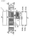
- Fig. 7 there is shown another example of the configuration of the non-feeding element 4.
- a surface-mounted antenna 1 shown in Fig. 7 except for the non-feeding element 4, the other structural parts of the antenna 1 are the same as those used in the surface-mounted antenna 1 shown in Fig. 1.
- Fig. 7 the same structural parts as those of the surface-mounted antenna 1 shown in Fig. 1 are indicated by the same reference numerals.
- a non-feeding-side first radiation electrode 8 is extended from a ground terminal 6 to a right side surface 2c via an upper surface 2a of a dielectric base member 2.
- a non-feeding-side second radiation electrode 9 is extended from the ground terminal 6 to a front side surface 2b of the dielectric base member 2.
- the non-feeding-side first and second radiation electrodes 8 and 9 may be disposed on different surfaces of the dielectric base member 2.
- the feeding element 3 and the non-feeding element 4 are branched elements composed of radiation electrodes formed by branching into two parts.
- the number of radiation electrodes forming each of branched elements may be three or more.
- the meandering pattern 15 as the fundamental-wave controlling unit is formed in the maximum resonance current region Z1 of the fundamental wave on the feeding-side radiation electrode 7, and the meandering pattern 16 as the harmonic controlling unit is formed in the maximum resonance current region Z2 of the second-order wave thereof.
- a fundamental-wave-controlling unit and a harmonic-controlling unit having structures different from those of the meandering patterns 15 and 16.
- a series inductance component may be locally added to the maximum resonance current region Z1 of the fundamental wave
- a series inductance component may be locally added to the maximum resonance current region Z2 of the second-order harmonic, by which an electric length per unit length in each of the regions Z1 and Z2 can be increased.
- dielectric members having permeabilities larger than in the other regions as a fundamental-wave controlling unit and a harmonic controlling unit.
- both of the fundamental-wave-controlling unit and the harmonic controlling unit are provided on the feeding-side radiation electrode 7.
- only one of the controlling units may be provided on the feeding-side radiation electrode 7.
- the feeding element 3 is formed as a branched element having two radiation electrodes 20 and 21.
- the radiation electrode 20 nor the radiation electrode 21 has the fundamental-wave-controlling unit and the harmonic controlling unit as shown in the first embodiment.
- one or both of the two radiation electrodes 20 and 21 may have at least one of the fundamental-wave-controlling unit and the harmonic controlling unit as shown above.
- the radiation electrodes 8 and 9 forming the non-feeding element 4 one or both of the radiation electrodes 8 and 9 may have at least one of the fundamental-wave-controlling unit and the harmonic controlling unit.
- one or more of the plurality of radiation electrodes forming the feeding element 3 and the non-feeding element 4 may have at least one of the fundamental-wave controlling unit and the harmonic-controlling unit disposed thereon.
- the present invention can also be applied to a surface-mounted antenna 1 of a capacitance feeding type, in which electrical power is supplied to the feeding terminal 5 by capacitive coupling.
- the present invention can also be applied to an installed-type wireless device.
- the feeding element and the non-feeding element are formed as branched elements, at least three or more radiation electrodes are formed in the single surface-mounted antenna.
- the antenna is easily adaptable to multi-bands.
- the plurality of radiation electrodes forming the branched elements is extended from the feeding terminal and the ground terminal in the directions in which the distance between the radiation electrodes is expanded. As a result, the mutual interference between the plurality of radiation electrodes forming the branched elements can be prevented.
- the resonance waves of the radiation electrodes can be controlled independently from each other, the radiation electrodes can be easily designed and the freedom of designing can be increased. Moreover, reliability of the antenna characteristics can be increased.
- the resonant frequencies of the fundamental wave and the harmonic can be controlled.
- the fundamental-wave controlling unit is locally disposed in the maximum resonance current region of the fundamental wave on the current path of the radiation electrode
- the harmonic controlling unit is locally disposed in the maximum resonance current region of the harmonic on the current path of the radiation electrode
- the frequency of the resonance wave of one of the fundamental wave and the harmonic can be controlled in a state substantially independent from the other resonance wave.
- the difference between the resonant frequencies of the fundamental wave and the harmonic can be significantly changed and controlled.
- the difference between the resonant frequencies thereof can be controlled with high precision, when the series inductance component is locally added to the maximum resonance current region of at least one of the fundamental wave and the harmonic in the feeding element of the surface-mounted antenna to form the region of a large electrical length.
- the frequency band can be easily broadened.
- broadening of the frequency band can be achieved by bringing only the frequency band selected from the plurality of required frequency bands into a multi-resonance state.
- the capacitive-feeding-type surface-mounted antenna can provide the same advantages as described above in terms of easy adaptability to multi-bands.
- the wireless device incorporating the surface-mounted antenna having the unique structure in accordance with the present invention as described above, with only the single surface-mounted antenna provided, the wireless device is easily adaptable to multi-bands.
- the wireless device of the invention can have highly reliable antenna characteristics.
Applications Claiming Priority (2)
| Application Number | Priority Date | Filing Date | Title |
|---|---|---|---|
| JP2000108851A JP3658639B2 (ja) | 2000-04-11 | 2000-04-11 | 表面実装型アンテナおよびそのアンテナを備えた無線機 |
| JP2000108851 | 2000-04-11 |
Publications (3)
| Publication Number | Publication Date |
|---|---|
| EP1146590A2 true EP1146590A2 (de) | 2001-10-17 |
| EP1146590A3 EP1146590A3 (de) | 2003-09-03 |
| EP1146590B1 EP1146590B1 (de) | 2007-01-03 |
Family
ID=18621627
Family Applications (1)
| Application Number | Title | Priority Date | Filing Date |
|---|---|---|---|
| EP01107520A Expired - Lifetime EP1146590B1 (de) | 2000-04-11 | 2001-03-26 | Oberflächenmontierte Antenne und Funkgerät mit einer derartigen Antenne |
Country Status (6)
| Country | Link |
|---|---|
| US (1) | US6433745B1 (de) |
| EP (1) | EP1146590B1 (de) |
| JP (1) | JP3658639B2 (de) |
| KR (1) | KR100414634B1 (de) |
| CN (1) | CN1165098C (de) |
| DE (1) | DE60125632T2 (de) |
Cited By (20)
| Publication number | Priority date | Publication date | Assignee | Title |
|---|---|---|---|---|
| EP1204160A2 (de) * | 2000-10-09 | 2002-05-08 | Philips Corporate Intellectual Property GmbH | Mehrband-Mikrowellenantenne |
| WO2002089249A1 (fr) * | 2001-04-23 | 2002-11-07 | Yokowo Co., Ltd. | Antenne a large bande pour communication de service mobile |
| GB2380326A (en) * | 2001-06-20 | 2003-04-02 | Murata Manufacturing Co | Substrate antenna with fed and non-fed elements having slits |
| WO2003047031A1 (en) * | 2001-11-26 | 2003-06-05 | Telefonaktiebolaget Lm Ericsson (Publ) | Compact broadband antenna |
| EP1367671A2 (de) * | 2002-05-28 | 2003-12-03 | Ngk Spark Plug Co., Ltd | Mäanderförmige Mehrbandantenne |
| WO2005086287A1 (en) * | 2004-02-25 | 2005-09-15 | Philips Intellectual Property & Standards Gmbh | Antenna module |
| WO2005091430A2 (en) * | 2004-03-16 | 2005-09-29 | Antenova Limited | Dielectric antenna with metallised walls |
| US6963308B2 (en) | 2003-01-15 | 2005-11-08 | Filtronic Lk Oy | Multiband antenna |
| WO2006084951A1 (en) | 2005-02-08 | 2006-08-17 | Pulse Finland Oy | Internal monopole antenna |
| EP1835563A1 (de) * | 2005-01-05 | 2007-09-19 | Murata Manufacturing Co., Ltd. | Antennenstruktur und drahtlose kommunikationseinheit damit |
| WO2008030286A1 (en) * | 2006-09-05 | 2008-03-13 | Apple Inc. | Tunable antennas for handheld devices |
| WO2010000500A1 (en) * | 2008-07-03 | 2010-01-07 | Sony Ericsson Mobile Communications Ab | Broadband antenna |
| US7808435B2 (en) | 2006-02-14 | 2010-10-05 | Murata Manufacturing Co., Ltd. | Antenna structure and wireless communication apparatus including same |
| EP2192653A3 (de) * | 2008-11-26 | 2011-08-17 | TDK Corporation | Auf einer Leiterplatte oberflächenmontierte Antenne und deren Herstellungsverfahren |
| DE102005040499B4 (de) * | 2004-08-26 | 2011-08-18 | Kyocera Corp. | Oberflächenmontierte Antenne und diese verwendende Antennenvorrichtung sowie Drahtloskommunikationsvorrichtung |
| EP2741366A4 (de) * | 2012-08-28 | 2015-02-25 | Murata Manufacturing Co | Antennenvorrichtung und kommunikationsendgerät |
| GB2486362B (en) * | 2009-08-27 | 2015-02-25 | Murata Manufacturing Co | Flexible substrate antenna and antenna device |
| US9293828B2 (en) | 2013-03-27 | 2016-03-22 | Apple Inc. | Antenna system with tuning from coupled antenna |
| EP1856764B1 (de) * | 2004-12-31 | 2016-04-27 | Nokia Technologies Oy | Interne mehrband-antenne mit planaren streifenelementen |
| US10355339B2 (en) | 2013-03-18 | 2019-07-16 | Apple Inc. | Tunable antenna with slot-based parasitic element |
Families Citing this family (43)
| Publication number | Priority date | Publication date | Assignee | Title |
|---|---|---|---|---|
| KR100444217B1 (ko) * | 2001-09-12 | 2004-08-16 | 삼성전기주식회사 | 표면실장형 칩 안테나 |
| KR100532223B1 (ko) * | 2002-05-15 | 2005-11-29 | (주) 코산아이엔티 | 마이크로 칩 듀얼밴드 안테나 |
| JP2004201278A (ja) * | 2002-12-06 | 2004-07-15 | Sharp Corp | パターンアンテナ |
| JP3825400B2 (ja) * | 2002-12-13 | 2006-09-27 | 京セラ株式会社 | アンテナ装置 |
| JP2004242159A (ja) | 2003-02-07 | 2004-08-26 | Ngk Spark Plug Co Ltd | 高周波アンテナモジュール |
| EP1538703B1 (de) | 2003-06-09 | 2009-02-11 | Panasonic Corporation | Antenne und elektronisches gerät |
| WO2005029642A1 (ja) * | 2003-09-22 | 2005-03-31 | Anten Corporation | 多周波数共用アンテナ |
| EP1978595B1 (de) * | 2003-12-25 | 2011-03-23 | Mitsubishi Materials Corporation | Antennenvorrichtung und Kommunikationsgerät |
| US8155721B2 (en) | 2004-01-12 | 2012-04-10 | Erchonia Corporation | Method and device for reducing undesirable electromagnetic radiation |
| US7800554B2 (en) * | 2008-06-26 | 2010-09-21 | Erchonia Corporation | Varying angle antenna for electromagnetic radiation dissipation device |
| JP2007524310A (ja) * | 2004-02-18 | 2007-08-23 | コーニンクレッカ フィリップス エレクトロニクス エヌ ヴィ | アンテナ |
| TWI239678B (en) * | 2004-05-14 | 2005-09-11 | Benq Corp | Antenna device and mobile unit using the same |
| CN100379085C (zh) * | 2004-06-22 | 2008-04-02 | 明基电通股份有限公司 | 天线装置与利用此装置的移动单元 |
| KR20070016545A (ko) | 2005-08-04 | 2007-02-08 | 삼성전자주식회사 | 휴대용 단말기의 안테나 장치 |
| US7161540B1 (en) * | 2005-08-24 | 2007-01-09 | Accton Technology Corporation | Dual-band patch antenna |
| FI118782B (fi) * | 2005-10-14 | 2008-03-14 | Pulse Finland Oy | Säädettävä antenni |
| US20070114889A1 (en) * | 2005-11-21 | 2007-05-24 | Honeywell International | Chip level packaging for wireless surface acoustic wave sensor |
| US7477195B2 (en) * | 2006-03-07 | 2009-01-13 | Sony Ericsson Mobile Communications Ab | Multi-frequency band antenna device for radio communication terminal |
| KR100808811B1 (ko) * | 2006-04-13 | 2008-03-03 | (주)모토닉스 | 차량용 다중대역 안테나 |
| KR100664552B1 (ko) | 2006-05-25 | 2007-01-03 | 주식회사 모비너스 | 이동통신 단말기용 다중대역 칩 안테나 |
| US7761115B2 (en) * | 2006-05-30 | 2010-07-20 | Broadcom Corporation | Multiple mode RF transceiver and antenna structure |
| FI119268B (fi) * | 2006-08-25 | 2008-09-15 | Pulse Finland Oy | Moniresonanssiantenni |
| KR100867128B1 (ko) * | 2007-01-04 | 2008-11-06 | 주식회사 이엠따블유안테나 | 이중 대역 안테나 |
| JP4752771B2 (ja) * | 2007-01-19 | 2011-08-17 | 株式会社村田製作所 | アンテナ構造の不要波放射抑制方法およびアンテナ構造およびそれを備えた無線通信装置 |
| CN101573831B (zh) * | 2007-01-19 | 2012-11-21 | 株式会社村田制作所 | 天线装置及无线通信机 |
| US7542009B2 (en) * | 2007-03-05 | 2009-06-02 | United Microelectronics Corp. | Wireless communication device and signal receiving/transmitting method thereof |
| JP4661816B2 (ja) * | 2007-03-30 | 2011-03-30 | 株式会社村田製作所 | アンテナおよび無線通信機 |
| US7450076B1 (en) * | 2007-06-28 | 2008-11-11 | Cheng Uei Precision Industry Co., Ltd. | Integrated multi-band antenna |
| CN101836329B (zh) * | 2007-10-26 | 2012-12-19 | Tdk株式会社 | 天线装置及使用该天线装置的无线通信机 |
| JP5777885B2 (ja) * | 2008-01-08 | 2015-09-09 | エース テクノロジーズ コーポレーション | 多重帯域内蔵型アンテナ |
| US9190735B2 (en) * | 2008-04-04 | 2015-11-17 | Tyco Electronics Services Gmbh | Single-feed multi-cell metamaterial antenna devices |
| KR20100030522A (ko) * | 2008-09-10 | 2010-03-18 | (주)에이스안테나 | 전자기적 커플링을 이용한 다중 대역 안테나 |
| JP4784636B2 (ja) * | 2008-10-28 | 2011-10-05 | Tdk株式会社 | 表面実装型アンテナ及びこれを用いるアンテナ装置並びに無線通信機 |
| CN102763274B (zh) * | 2010-02-24 | 2015-07-01 | 夏普株式会社 | 天线组件以及便携式无线终端 |
| JP2012060380A (ja) * | 2010-09-08 | 2012-03-22 | Alps Electric Co Ltd | アンテナ装置 |
| JP2012227876A (ja) * | 2011-04-22 | 2012-11-15 | Tdk Corp | アンテナ装置及びこれを用いた無線通信機器 |
| US9583824B2 (en) * | 2011-09-28 | 2017-02-28 | Sony Corporation | Multi-band wireless terminals with a hybrid antenna along an end portion, and related multi-band antenna systems |
| US9673520B2 (en) * | 2011-09-28 | 2017-06-06 | Sony Corporation | Multi-band wireless terminals with multiple antennas along an end portion, and related multi-band antenna systems |
| KR101378847B1 (ko) | 2012-07-27 | 2014-03-27 | 엘에스엠트론 주식회사 | 광대역 특성을 갖는 내장형 안테나 |
| US9627747B2 (en) * | 2012-11-28 | 2017-04-18 | The Board Of Trustees Of The University Of Alabama For And On Behalf Of The University Of Alabama | Dual-polarized magnetic antennas |
| US9559433B2 (en) | 2013-03-18 | 2017-01-31 | Apple Inc. | Antenna system having two antennas and three ports |
| US9444130B2 (en) | 2013-04-10 | 2016-09-13 | Apple Inc. | Antenna system with return path tuning and loop element |
| JP5726983B2 (ja) * | 2013-10-30 | 2015-06-03 | 太陽誘電株式会社 | チップ状アンテナ装置及び送受信用通信回路基板 |
Citations (5)
| Publication number | Priority date | Publication date | Assignee | Title |
|---|---|---|---|---|
| JPH09260934A (ja) * | 1996-03-26 | 1997-10-03 | Matsushita Electric Works Ltd | マイクロストリップアンテナ |
| WO1999003168A1 (en) * | 1997-07-09 | 1999-01-21 | Allgon Ab | Trap microstrip pifa |
| EP0965152A1 (de) * | 1997-02-25 | 1999-12-22 | Pates Technology Patentverwertungsgesellschaft Für Satelliten- Und Moderne Informationstechnologien Mbh | Resonanzantenne |
| EP1063722A2 (de) * | 1999-06-25 | 2000-12-27 | Murata Manufacturing Co., Ltd. | Antennenanordnung und Kommunikationsgerät mit einer derartigen Antenne |
| EP1143558A2 (de) * | 2000-03-30 | 2001-10-10 | Murata Manufacturing Co., Ltd. | Oberflächenmontierte Antenne, Verfahren zur Justierung und Einstellung der Zweifrequenzresonanz der Antenne und Kommunikationsgerät mit einer derartigen Antenne |
Family Cites Families (13)
| Publication number | Priority date | Publication date | Assignee | Title |
|---|---|---|---|---|
| JPH07131234A (ja) * | 1993-11-02 | 1995-05-19 | Nippon Mektron Ltd | 複共振アンテナ |
| US5748149A (en) * | 1995-10-04 | 1998-05-05 | Murata Manufacturing Co., Ltd. | Surface mounting antenna and antenna apparatus |
| JP3319268B2 (ja) * | 1996-02-13 | 2002-08-26 | 株式会社村田製作所 | 表面実装型アンテナおよびこれを用いた通信機 |
| JP3114605B2 (ja) * | 1996-02-14 | 2000-12-04 | 株式会社村田製作所 | 表面実装型アンテナおよびこれを用いた通信機 |
| JP3114621B2 (ja) * | 1996-06-19 | 2000-12-04 | 株式会社村田製作所 | 表面実装型アンテナおよびこれを用いた通信機 |
| AU731954B2 (en) * | 1996-07-03 | 2001-04-05 | Radio Frequency Systems Inc. | Log periodic dipole antenna having a microstrip feedline |
| JP3279205B2 (ja) * | 1996-12-10 | 2002-04-30 | 株式会社村田製作所 | 表面実装型アンテナおよび通信機 |
| JPH11127014A (ja) * | 1997-10-23 | 1999-05-11 | Mitsubishi Materials Corp | アンテナ装置 |
| KR100294979B1 (ko) * | 1998-06-12 | 2001-07-12 | 김춘호 | 다중대역세라믹칩안테나 |
| JP3351363B2 (ja) * | 1998-11-17 | 2002-11-25 | 株式会社村田製作所 | 表面実装型アンテナおよびそれを用いた通信装置 |
| JP3639767B2 (ja) * | 1999-06-24 | 2005-04-20 | 株式会社村田製作所 | 表面実装型アンテナおよびそれを用いた通信機 |
| JP3562512B2 (ja) * | 1999-09-30 | 2004-09-08 | 株式会社村田製作所 | 表面実装型アンテナおよびそのアンテナを備えた通信装置 |
| JP3528737B2 (ja) * | 2000-02-04 | 2004-05-24 | 株式会社村田製作所 | 表面実装型アンテナおよびその調整方法および表面実装型アンテナを備えた通信装置 |
-
2000
- 2000-04-11 JP JP2000108851A patent/JP3658639B2/ja not_active Expired - Lifetime
-
2001
- 2001-03-26 DE DE60125632T patent/DE60125632T2/de not_active Expired - Lifetime
- 2001-03-26 EP EP01107520A patent/EP1146590B1/de not_active Expired - Lifetime
- 2001-04-11 CN CNB011168277A patent/CN1165098C/zh not_active Expired - Lifetime
- 2001-04-11 KR KR10-2001-0019247A patent/KR100414634B1/ko active IP Right Grant
- 2001-04-11 US US09/832,714 patent/US6433745B1/en not_active Expired - Lifetime
Patent Citations (5)
| Publication number | Priority date | Publication date | Assignee | Title |
|---|---|---|---|---|
| JPH09260934A (ja) * | 1996-03-26 | 1997-10-03 | Matsushita Electric Works Ltd | マイクロストリップアンテナ |
| EP0965152A1 (de) * | 1997-02-25 | 1999-12-22 | Pates Technology Patentverwertungsgesellschaft Für Satelliten- Und Moderne Informationstechnologien Mbh | Resonanzantenne |
| WO1999003168A1 (en) * | 1997-07-09 | 1999-01-21 | Allgon Ab | Trap microstrip pifa |
| EP1063722A2 (de) * | 1999-06-25 | 2000-12-27 | Murata Manufacturing Co., Ltd. | Antennenanordnung und Kommunikationsgerät mit einer derartigen Antenne |
| EP1143558A2 (de) * | 2000-03-30 | 2001-10-10 | Murata Manufacturing Co., Ltd. | Oberflächenmontierte Antenne, Verfahren zur Justierung und Einstellung der Zweifrequenzresonanz der Antenne und Kommunikationsgerät mit einer derartigen Antenne |
Non-Patent Citations (1)
| Title |
|---|
| PATENT ABSTRACTS OF JAPAN vol. 1998, no. 02, 30 January 1998 (1998-01-30) & JP 09 260934 A (MATSUSHITA ELECTRIC WORKS LTD), 3 October 1997 (1997-10-03) * |
Cited By (35)
| Publication number | Priority date | Publication date | Assignee | Title |
|---|---|---|---|---|
| EP1204160A2 (de) * | 2000-10-09 | 2002-05-08 | Philips Corporate Intellectual Property GmbH | Mehrband-Mikrowellenantenne |
| EP1204160A3 (de) * | 2000-10-09 | 2004-01-07 | Philips Intellectual Property & Standards GmbH | Mehrband-Mikrowellenantenne |
| US6922172B2 (en) | 2001-04-23 | 2005-07-26 | Yokowo Co., Ltd. | Broad-band antenna for mobile communication |
| WO2002089249A1 (fr) * | 2001-04-23 | 2002-11-07 | Yokowo Co., Ltd. | Antenne a large bande pour communication de service mobile |
| GB2380326A (en) * | 2001-06-20 | 2003-04-02 | Murata Manufacturing Co | Substrate antenna with fed and non-fed elements having slits |
| GB2380326B (en) * | 2001-06-20 | 2003-11-26 | Murata Manufacturing Co | Surface mount type antenna and radio transmitter and receiver using the same |
| WO2003047031A1 (en) * | 2001-11-26 | 2003-06-05 | Telefonaktiebolaget Lm Ericsson (Publ) | Compact broadband antenna |
| US6650294B2 (en) | 2001-11-26 | 2003-11-18 | Telefonaktiebolaget Lm Ericsson (Publ) | Compact broadband antenna |
| EP1367671A3 (de) * | 2002-05-28 | 2005-02-09 | Ngk Spark Plug Co., Ltd | Mäanderförmige Mehrbandantenne |
| EP1617512A1 (de) * | 2002-05-28 | 2006-01-18 | Ngk Spark Plug Co., Ltd. | Mäanderförmige Mehrbandantenne |
| EP1367671A2 (de) * | 2002-05-28 | 2003-12-03 | Ngk Spark Plug Co., Ltd | Mäanderförmige Mehrbandantenne |
| US6963308B2 (en) | 2003-01-15 | 2005-11-08 | Filtronic Lk Oy | Multiband antenna |
| WO2005086287A1 (en) * | 2004-02-25 | 2005-09-15 | Philips Intellectual Property & Standards Gmbh | Antenna module |
| WO2005091430A2 (en) * | 2004-03-16 | 2005-09-29 | Antenova Limited | Dielectric antenna with metallised walls |
| WO2005091430A3 (en) * | 2004-03-16 | 2005-11-17 | Antenova Ltd | Dielectric antenna with metallised walls |
| DE102005040499B4 (de) * | 2004-08-26 | 2011-08-18 | Kyocera Corp. | Oberflächenmontierte Antenne und diese verwendende Antennenvorrichtung sowie Drahtloskommunikationsvorrichtung |
| EP1856764B1 (de) * | 2004-12-31 | 2016-04-27 | Nokia Technologies Oy | Interne mehrband-antenne mit planaren streifenelementen |
| EP1835563A1 (de) * | 2005-01-05 | 2007-09-19 | Murata Manufacturing Co., Ltd. | Antennenstruktur und drahtlose kommunikationseinheit damit |
| EP1835563A4 (de) * | 2005-01-05 | 2008-07-16 | Murata Manufacturing Co | Antennenstruktur und drahtlose kommunikationseinheit damit |
| US7538732B2 (en) | 2005-01-05 | 2009-05-26 | Murata Manufacturing Co., Ltd. | Antenna structure and radio communication apparatus including the same |
| WO2006084951A1 (en) | 2005-02-08 | 2006-08-17 | Pulse Finland Oy | Internal monopole antenna |
| EP1846982A4 (de) * | 2005-02-08 | 2008-12-31 | Lk Products Oy | Intern-monopol-antenne |
| EP1846982A1 (de) * | 2005-02-08 | 2007-10-24 | Lk-Products Oy | Intern-monopol-antenne |
| US7808435B2 (en) | 2006-02-14 | 2010-10-05 | Murata Manufacturing Co., Ltd. | Antenna structure and wireless communication apparatus including same |
| US7671804B2 (en) | 2006-09-05 | 2010-03-02 | Apple Inc. | Tunable antennas for handheld devices |
| WO2008030286A1 (en) * | 2006-09-05 | 2008-03-13 | Apple Inc. | Tunable antennas for handheld devices |
| WO2010000500A1 (en) * | 2008-07-03 | 2010-01-07 | Sony Ericsson Mobile Communications Ab | Broadband antenna |
| US7847746B2 (en) | 2008-07-03 | 2010-12-07 | Sony Ericsson Mobile Communications Ab | Broadband antenna |
| EP2192653A3 (de) * | 2008-11-26 | 2011-08-17 | TDK Corporation | Auf einer Leiterplatte oberflächenmontierte Antenne und deren Herstellungsverfahren |
| GB2486362B (en) * | 2009-08-27 | 2015-02-25 | Murata Manufacturing Co | Flexible substrate antenna and antenna device |
| US9608319B2 (en) | 2009-08-27 | 2017-03-28 | Murata Manufacturing Co., Ltd. | Flexible substrate antenna and antenna device |
| US9153865B2 (en) | 2012-08-28 | 2015-10-06 | Murata Manufacturing Co., Ltd. | Antenna device and communication terminal apparatus |
| EP2741366A4 (de) * | 2012-08-28 | 2015-02-25 | Murata Manufacturing Co | Antennenvorrichtung und kommunikationsendgerät |
| US10355339B2 (en) | 2013-03-18 | 2019-07-16 | Apple Inc. | Tunable antenna with slot-based parasitic element |
| US9293828B2 (en) | 2013-03-27 | 2016-03-22 | Apple Inc. | Antenna system with tuning from coupled antenna |
Also Published As
| Publication number | Publication date |
|---|---|
| JP3658639B2 (ja) | 2005-06-08 |
| US6433745B1 (en) | 2002-08-13 |
| CN1165098C (zh) | 2004-09-01 |
| US20020030626A1 (en) | 2002-03-14 |
| KR100414634B1 (ko) | 2004-01-07 |
| JP2001298313A (ja) | 2001-10-26 |
| EP1146590B1 (de) | 2007-01-03 |
| KR20010098511A (ko) | 2001-11-08 |
| CN1322033A (zh) | 2001-11-14 |
| DE60125632D1 (de) | 2007-02-15 |
| EP1146590A3 (de) | 2003-09-03 |
| DE60125632T2 (de) | 2007-05-03 |
Similar Documents
| Publication | Publication Date | Title |
|---|---|---|
| US6433745B1 (en) | Surface-mounted antenna and wireless device incorporating the same | |
| KR100396180B1 (ko) | 표면 실장형 안테나 및 이를 포함하는 통신 장치 | |
| US6466170B2 (en) | Internal multi-band antennas for mobile communications | |
| EP1346436B1 (de) | Antennenanordnung | |
| JP4423809B2 (ja) | 複共振アンテナ | |
| EP1290757B1 (de) | Konvertierbare dipol-/invertierte f-antennen und drahtlose kommunikationsgeräte mit derartigen antennen | |
| US7119749B2 (en) | Antenna and radio communication apparatus | |
| EP2387101B1 (de) | Tragbare mobile Kommunikationsvorrichtungen mit Antennenarray und mehreren hochisolierten Anschlüssen | |
| EP2628209B1 (de) | Eine rahmenantenne für mobilteile und andere anwendungen | |
| JP4858860B2 (ja) | マルチバンドアンテナ | |
| KR101188465B1 (ko) | 다중 대역 무선 디바이스용 안테나 장치 및 관련 방법 | |
| WO2001091234A1 (en) | Convertible loop/inverted-f antennas and wireless communicators incorporating the same | |
| EP1411586A1 (de) | Tragbare funkverwendungsantenne | |
| KR20090115063A (ko) | 안테나 및 그 안테나를 포함하는 통신 장치 | |
| JPWO2004109850A1 (ja) | 周波数可変型アンテナおよびそれを備えた通信機 | |
| EP2071668A1 (de) | Antenne und mobilfunkkommunikationsgerät | |
| JP2006512003A (ja) | 携帯型無線機器用小体積アンテナ | |
| WO2001008257A1 (en) | Antenna arrangement | |
| JP3828504B2 (ja) | 無線装置 | |
| US20190181556A1 (en) | Antenna for a Portable Communication Device | |
| JPH09232854A (ja) | 移動無線機用小型平面アンテナ装置 | |
| KR100834672B1 (ko) | 휴대단말기 | |
| FI114260B (fi) | Radiolaitteen modulaarinen kytkentärakenne ja kannettava radiolaite | |
| JP4232626B2 (ja) | アンテナ装置 |
Legal Events
| Date | Code | Title | Description |
|---|---|---|---|
| PUAI | Public reference made under article 153(3) epc to a published international application that has entered the european phase |
Free format text: ORIGINAL CODE: 0009012 |
|
| 17P | Request for examination filed |
Effective date: 20010326 |
|
| AK | Designated contracting states |
Kind code of ref document: A2 Designated state(s): AT BE CH CY DE DK ES FI FR GB GR IE IT LI LU MC NL PT SE TR |
|
| AX | Request for extension of the european patent |
Free format text: AL;LT;LV;MK;RO;SI |
|
| PUAL | Search report despatched |
Free format text: ORIGINAL CODE: 0009013 |
|
| AK | Designated contracting states |
Kind code of ref document: A3 Designated state(s): AT BE CH CY DE DK ES FI FR GB GR IE IT LI LU MC NL PT SE TR |
|
| AX | Request for extension of the european patent |
Extension state: AL LT LV MK RO SI |
|
| 17Q | First examination report despatched |
Effective date: 20031107 |
|
| AKX | Designation fees paid |
Designated state(s): DE FR GB IT |
|
| GRAP | Despatch of communication of intention to grant a patent |
Free format text: ORIGINAL CODE: EPIDOSNIGR1 |
|
| GRAS | Grant fee paid |
Free format text: ORIGINAL CODE: EPIDOSNIGR3 |
|
| GRAA | (expected) grant |
Free format text: ORIGINAL CODE: 0009210 |
|
| AK | Designated contracting states |
Kind code of ref document: B1 Designated state(s): DE FR GB IT |
|
| REG | Reference to a national code |
Ref country code: GB Ref legal event code: FG4D |
|
| REF | Corresponds to: |
Ref document number: 60125632 Country of ref document: DE Date of ref document: 20070215 Kind code of ref document: P |
|
| EN | Fr: translation not filed | ||
| RAP2 | Party data changed (patent owner data changed or rights of a patent transferred) |
Owner name: MURATA MANUFACTURING CO., LTD. |
|
| PLBE | No opposition filed within time limit |
Free format text: ORIGINAL CODE: 0009261 |
|
| STAA | Information on the status of an ep patent application or granted ep patent |
Free format text: STATUS: NO OPPOSITION FILED WITHIN TIME LIMIT |
|
| 26N | No opposition filed |
Effective date: 20071005 |
|
| GBPC | Gb: european patent ceased through non-payment of renewal fee |
Effective date: 20070403 |
|
| PG25 | Lapsed in a contracting state [announced via postgrant information from national office to epo] |
Ref country code: GB Free format text: LAPSE BECAUSE OF NON-PAYMENT OF DUE FEES Effective date: 20070403 Ref country code: FR Free format text: LAPSE BECAUSE OF FAILURE TO SUBMIT A TRANSLATION OF THE DESCRIPTION OR TO PAY THE FEE WITHIN THE PRESCRIBED TIME-LIMIT Effective date: 20070824 Ref country code: IT Free format text: LAPSE BECAUSE OF FAILURE TO SUBMIT A TRANSLATION OF THE DESCRIPTION OR TO PAY THE FEE WITHIN THE PRESCRIBED TIME-LIMIT Effective date: 20070103 |
|
| PG25 | Lapsed in a contracting state [announced via postgrant information from national office to epo] |
Ref country code: FR Free format text: LAPSE BECAUSE OF FAILURE TO SUBMIT A TRANSLATION OF THE DESCRIPTION OR TO PAY THE FEE WITHIN THE PRESCRIBED TIME-LIMIT Effective date: 20070103 |
|
| PGFP | Annual fee paid to national office [announced via postgrant information from national office to epo] |
Ref country code: DE Payment date: 20200320 Year of fee payment: 20 |
|
| REG | Reference to a national code |
Ref country code: DE Ref legal event code: R071 Ref document number: 60125632 Country of ref document: DE |