EP1143558A2 - Oberflächenmontierte Antenne, Verfahren zur Justierung und Einstellung der Zweifrequenzresonanz der Antenne und Kommunikationsgerät mit einer derartigen Antenne - Google Patents
Oberflächenmontierte Antenne, Verfahren zur Justierung und Einstellung der Zweifrequenzresonanz der Antenne und Kommunikationsgerät mit einer derartigen Antenne Download PDFInfo
- Publication number
- EP1143558A2 EP1143558A2 EP01107082A EP01107082A EP1143558A2 EP 1143558 A2 EP1143558 A2 EP 1143558A2 EP 01107082 A EP01107082 A EP 01107082A EP 01107082 A EP01107082 A EP 01107082A EP 1143558 A2 EP1143558 A2 EP 1143558A2
- Authority
- EP
- European Patent Office
- Prior art keywords
- radiation electrode
- radiation
- high current
- regions
- field
- Prior art date
- Legal status (The legal status is an assumption and is not a legal conclusion. Google has not performed a legal analysis and makes no representation as to the accuracy of the status listed.)
- Granted
Links
- 238000004891 communication Methods 0.000 title claims abstract description 36
- 238000000034 method Methods 0.000 title claims description 34
- 230000005855 radiation Effects 0.000 claims abstract description 562
- 230000005684 electric field Effects 0.000 claims abstract description 200
- 238000010168 coupling process Methods 0.000 claims abstract description 184
- 238000005859 coupling reaction Methods 0.000 claims abstract description 184
- 230000008878 coupling Effects 0.000 claims abstract description 183
- 230000009977 dual effect Effects 0.000 claims abstract description 107
- 239000000758 substrate Substances 0.000 claims description 47
- 238000013461 design Methods 0.000 description 10
- 238000010586 diagram Methods 0.000 description 10
- 230000000694 effects Effects 0.000 description 8
- 238000002474 experimental method Methods 0.000 description 8
- 238000010276 construction Methods 0.000 description 7
- 238000004519 manufacturing process Methods 0.000 description 5
- 230000009467 reduction Effects 0.000 description 4
- 230000002829 reductive effect Effects 0.000 description 4
- 230000008054 signal transmission Effects 0.000 description 4
- 230000005540 biological transmission Effects 0.000 description 3
- 230000002401 inhibitory effect Effects 0.000 description 3
- 230000006872 improvement Effects 0.000 description 2
- 238000012986 modification Methods 0.000 description 2
- 230000004048 modification Effects 0.000 description 2
- 238000009966 trimming Methods 0.000 description 2
- 238000013459 approach Methods 0.000 description 1
- 230000002238 attenuated effect Effects 0.000 description 1
- 230000001413 cellular effect Effects 0.000 description 1
- 230000003247 decreasing effect Effects 0.000 description 1
- 238000011161 development Methods 0.000 description 1
- 238000007781 pre-processing Methods 0.000 description 1
- 238000012827 research and development Methods 0.000 description 1
Images


Classifications
-
- H—ELECTRICITY
- H01—ELECTRIC ELEMENTS
- H01Q—ANTENNAS, i.e. RADIO AERIALS
- H01Q1/00—Details of, or arrangements associated with, antennas
- H01Q1/12—Supports; Mounting means
- H01Q1/22—Supports; Mounting means by structural association with other equipment or articles
- H01Q1/24—Supports; Mounting means by structural association with other equipment or articles with receiving set
-
- H—ELECTRICITY
- H01—ELECTRIC ELEMENTS
- H01Q—ANTENNAS, i.e. RADIO AERIALS
- H01Q19/00—Combinations of primary active antenna elements and units with secondary devices, e.g. with quasi-optical devices, for giving the antenna a desired directional characteristic
- H01Q19/005—Patch antenna using one or more coplanar parasitic elements
-
- H—ELECTRICITY
- H01—ELECTRIC ELEMENTS
- H01Q—ANTENNAS, i.e. RADIO AERIALS
- H01Q1/00—Details of, or arrangements associated with, antennas
- H01Q1/12—Supports; Mounting means
- H01Q1/22—Supports; Mounting means by structural association with other equipment or articles
- H01Q1/24—Supports; Mounting means by structural association with other equipment or articles with receiving set
- H01Q1/241—Supports; Mounting means by structural association with other equipment or articles with receiving set used in mobile communications, e.g. GSM
- H01Q1/242—Supports; Mounting means by structural association with other equipment or articles with receiving set used in mobile communications, e.g. GSM specially adapted for hand-held use
- H01Q1/243—Supports; Mounting means by structural association with other equipment or articles with receiving set used in mobile communications, e.g. GSM specially adapted for hand-held use with built-in antennas
-
- H—ELECTRICITY
- H01—ELECTRIC ELEMENTS
- H01Q—ANTENNAS, i.e. RADIO AERIALS
- H01Q1/00—Details of, or arrangements associated with, antennas
- H01Q1/36—Structural form of radiating elements, e.g. cone, spiral, umbrella; Particular materials used therewith
- H01Q1/38—Structural form of radiating elements, e.g. cone, spiral, umbrella; Particular materials used therewith formed by a conductive layer on an insulating support
-
- H—ELECTRICITY
- H01—ELECTRIC ELEMENTS
- H01Q—ANTENNAS, i.e. RADIO AERIALS
- H01Q5/00—Arrangements for simultaneous operation of antennas on two or more different wavebands, e.g. dual-band or multi-band arrangements
- H01Q5/30—Arrangements for providing operation on different wavebands
- H01Q5/378—Combination of fed elements with parasitic elements
- H01Q5/385—Two or more parasitic elements
-
- H—ELECTRICITY
- H01—ELECTRIC ELEMENTS
- H01Q—ANTENNAS, i.e. RADIO AERIALS
- H01Q9/00—Electrically-short antennas having dimensions not more than twice the operating wavelength and consisting of conductive active radiating elements
- H01Q9/04—Resonant antennas
- H01Q9/0407—Substantially flat resonant element parallel to ground plane, e.g. patch antenna
Definitions
- the present invention relates to a surface-mounted type antenna incorporated in a communication device such as a portable telephone, and to a method for adjusting and setting the dual-resonance frequency thereof.
- the present invention further relates to a communication device including the surface-mounted type antenna.
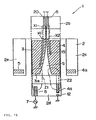
- Fig. 17 shows an example of a surface-mounted type antenna.
- the surface-mounted type antenna 1 shown in Fig. 17 is formed by juxtaposing a power supplied first radiation electrode 3 and a second radiation electrode 4 to which power is not directly supplied on a dielectric substrate 2 having a rectangular parallelepiped shape, with a space (slit) S therebetween.
- One end side of the first radiation electrode 3 is connected to a power supply portion (power supply terminal) 5, and the other end side thereof constitutes an open end 3a.
- One end side of the second radiation electrode 4 is connected to a short-circuit portion (ground short-circuit terminal) 6, and the other end side thereof constitutes an open end 4a.
- the first radiation electrode 3 and the second radiation electrode 4 each resonate, thereby performing an antenna operation (operation of signal transmission/reception).
- a widening of the frequency band of signal transmission/reception can be achieved.
- a surface-mounted type antenna 1 as described above is required to be miniaturized.
- the spacing between the first radiation electrode 3 and the second radiation electrode 4 is narrowed as an inevitable consequence.
- the electromagnetic coupling between the first radiation electrode 3 and the second radiation electrode 4 strengthens. This makes it difficult to stably achieve a desired dual-resonance state which allows a required antenna characteristic condition such as the widening of the frequency band to obtained.
- the electromagnetic coupling between the first radiation electrode 3 and the second radiation electrode 4 is controlled.
- the control of the electromagnetic coupling using the uniform-width space S is very difficult to execute, and provides a limited degree of flexibility in the design.
- the present invention has been made to solve the above-described problem, and aims to provide a surface-mounted type antenna which allows the miniaturization thereof and which is capable of easily meeting a required antenna characteristic condition, and to provide a method for adjusting and setting the dual resonance thereof, as well as a communication device including the surface-mounted type antenna.
- the present invention in a first aspect, provides a method for adjusting and setting the dual-resonance frequency of a surface-mounted type antenna which includes a dielectric substrate, a first radiation electrode to which power is supplied being formed on the top surface opposed to the mounting bottom-surface of the dielectric substrate, and a second radiation electrode which is juxtaposed with the first radiation electrode on the dielectric substrate with a space therebetween.
- This method comprises arranging the first radiation electrode and the second radiation electrode so that the strong electric-field regions of the first radiation electrode and the second radiation electrode wherein the electric fields of these radiation electrodes are each the strongest, are adjacent to each other, and so that the strong electric-field regions of these radiation electrodes thereby come into an electric-field coupling, simultaneously arranging the first radiation electrode and the second radiation electrode so that the high current regions of the first radiation electrode and the second radiation electrode wherein the currents of these radiation electrodes are each highest, are adjacent to each other, and so that the high current regions of these radiation electrodes thereby come into a magnetic-field coupling, variably adjusting each of the quantity of the electric-field coupling between the strong electric-field regions of the first radiation electrode and the second radiation electrode, and the quantity of the magnetic-field coupling between the high current regions of the first radiation electrode and the second radiation electrode, and setting the reflection loss of the dual resonance of the first radiation electrode and the second radiation electrode to a low value not higher than a predetermined value within the range of the set frequency, by adjusting both the
- the quantity of the electric-field coupling between the strong electric-field regions of the first radiation electrode and the second radiation electrode is variably adjusted, by making variable the spacing between the strong electric-field regions of the first radiation electrode and the second radiation electrode.
- the first radiation electrode be provided with a capacitance between the open end thereof which is the strong electric-field region thereof on one end side thereof and ground, that a power supply terminal or a ground short-circuit terminal be connected to the high current region thereof on the other end side thereof, while the second radiation electrode be provided with a capacitance between the open end thereof which is the strong electric-field region thereof on one end side thereof and ground, that a ground short-circuit terminal be connected to the high current region thereof on the other end side thereof, and the quantity of the electric-field coupling between the strong electric-field regions of the first radiation electrode and the second radiation electrode be relatively variably adjusted, by variably adjusting the capacitance between the open end of the first radiation electrode and ground, and the capacitance between the open end of the second radiation electrode and ground.
- the dielectric substrate be formed as a rectangular parallelepiped, and that the capacitive coupling portion between the open end of the strong electric-field region of the first radiation electrode and ground thereof and the capacitive coupling portion between the open end of the strong electric-field region of the second radiation electrode and ground thereof be each formed on mutually different surfaces of the dielectric substrate.
- the quantity of the magnetic-field coupling between the high current regions of the first radiation electrode and the second radiation electrode is variably adjusted, by making variable the spacing between the high current regions of these radiation electrodes.
- a conductive pattern be formed which is branched off from the power supply terminal or the ground short-circuit terminal of the first radiation electrode, and which is connected to ground, that a pattern for an inductance component addition be interposed in this conductive pattern, that a current path be formed which leads from the high current region of the first radiation electrode to the high current region of the second radiation electrode via the conductive pattern, ground, and the ground short-circuit terminal of the second radiation electrode, and that the quantity of the magnetic-field coupling between the high current regions of the first radiation electrode and the second radiation electrode be equivalently variably adjusted, by making variable the magnitude of the inductance component of the pattern for inductance component addition.
- the power supply terminal or the ground short-circuit terminal of the first radiation electrode and the ground short-circuit terminal of the second radiation electrode be juxtaposed with a spacing therebetween, that the power supply terminal or the ground short-circuit terminal of the first radiation electrode, and the ground short-circuit terminal of the second radiation electrode be short-circuited, by utilizing the pattern for inductance component addition, and that the quantity of the magnetic-field coupling between the high current regions of the first radiation electrode and the second radiation electrode be equivalently variably adjusted, by making variable the magnitude of the inductance component of the pattern for inductance component addition.
- the pattern for inductance component addition is made to also perform the function of an electrode pattern which constitutes a matching circuit.
- a surface-mounted type antenna comprising a dielectric substrate, a first radiation electrode to which power is applied formed on the surface of the dielectric substrate, and a second radiation electrode which is disposed adjacent to the first radiation electrode on the dielectric substrate with a spacing therebetween.
- the strong electric-field regions of the first radiation electrode and the second radiation electrode wherein each of the electric fields of these radiation electrodes is the strongest are disposed adjacent to each other with a spacing therebetween
- the high current regions of the first radiation electrode and the second radiation electrode wherein each of the currents of these radiation electrodes is the highest are disposed adjacent to each other with a spacing therebetween
- the space between the first radiation electrode and the second radiation electrode diverges from the high current region side to the strong electric-field region side.
- a power supply terminal or a ground short-circuit terminal is connected to the high current region of the first radiation electrode, a ground short-circuit terminal is connected to the high current region of the second radiation electrode, the power supply terminal or the ground short-circuit terminal of the first radiation electrode and the ground short-circuit terminal of the second radiation electrode are juxtaposed with a spacing therebetween.
- a pattern for inductance component addition which short-circuits the power supply terminal or the ground short-circuit terminal of the power supply radiation electrode and the ground short-circuit terminal of the second radiation electrode, be formed, that the magnitude of the inductance component of the pattern for inductance component addition be set to a value such as to allow the return loss characteristics in the dual resonance of the first radiation electrode and the second radiation electrode to be obtained, the return loss characteristics meeting a predetermined antenna characteristic condition, and that the resonance frequency of the first radiation electrode is lower than that of the second radiation electrode, in the frequency band of dual resonance.
- the present invention provides, in a third aspect, a communication device equipped with a surface-mounted type antenna produced by adjusting and setting the dual-resonance frequency using a method for adjusting and setting the dual-resonance frequency of a surface-mounted type antenna, in accordance with the first aspect, or a communication device equipped with a surface-mounted type antenna in accordance with the second aspect.
- the first radiation electrode and the second radiation electrode are arranged so that the strong electric-field regions of the first radiation electrode and the second radiation electrode are disposed adjacent to each other with a spacing therebetween, and are simultaneously arranged so that the high current regions of the first radiation electrode and the second radiation electrode are disposed adjacent to each other with a spacing therebetween.
- the present inventors discovered, during our research and development carried out on the surface-mounted type antenna, that the quantity of the electric-field coupling between the strong electric-field regions of the first radiation electrode and the second radiation electrode, and the quantity of the magnetic-field coupling between the high current regions of these radiation electrodes must both be in conditions suited for dual resonance, in order to achieve a dual-resonance state of the first radiation electrode and the second radiation electrode, the dual-resonance condition allowing an improvement in the antenna characteristics, such as the widening of the frequency band.
- each of the quantity of the electric-field coupling between the strong electric-field regions and the quantity of the magnetic-field coupling between the high current regions is variably adjusted, and both the quantities of the electric-field coupling and the magnetic-field coupling are set to conditions which allow return loss (reflection loss) characteristics in the dual resonance of the first radiation electrode and the second radiation electrode to be achieved, the return loss characteristics meeting a predetermined antenna characteristic condition such as the widening of the frequency band.
- the reflection loss in the dual resonance of the first radiation electrode and the second radiation electrode are set to a low value not higher than a predetermined value within the range of the set frequency. This allows a surface-mounted type antenna having required antenna characteristics to be obtained easily and in a short time.
- Fig. 1 is a schematic development view showing a surface-mounted type antenna in accordance with a first embodiment of the present invention.
- the parts having the same names as those of the conventional example has been given the same reference numerals.
- the surface-mounted type antenna 1 shown in Fig. 1 is constructed by forming electrode patterns such as a power supplied first radiation electrode 3 and a power non-supplied (power not directly supplied) second radiation electrode 4 on the surface of a dielectric substrate 2 having a rectangular parallelepiped shape.
- the radiation electrode to which power is supplied from a power supply is called the first radiation electrode.
- the radiation electrode to which power is supplied indirectly, i.e., by electro-magnetic coupling is called the second radiation electrode.
- This first embodiment is characterized in that the strong electric-field region Z1 in which the electric field of the first radiation electrode 3 is the strongest, and the strong electric-field region Z2 in which the electric field of the second radiation electrode 4 is the strongest, are disposed adjacent to each other, and that simultaneously the high current region X1 in which the current of the first radiation electrode 3 is the highest, and the high current region X2 in which the current of the second radiation electrode 4 is the highest, are disposed adjacent to each other.
- the first embodiment is further characterized in that the first radiation electrode 3 and the second radiation electrode 4 are arranged so as to create a dual resonance, and that the space S between the first radiation electrode 3 and the second radiation electrode 4 diverges from the above-described high current region X1 and X2 sides to the strong electric-field region Z1 and Z2 sides. Moreover, the first embodiment is characterized in that a meander-shaped pattern 9, which is capable of performing the function of an electrode pattern in a matching circuit, is formed on the dielectric substrate 2.
- the first radiation electrode 3 and the second radiation electrode 4 are juxtaposed on the top surface 2a of the dielectric substrate 2 with a space therebetween.
- a power supply terminal 5 and a short-circuit terminal 6, each of which vertically extends in the figure, are disposed adjacent to each other with a spacing therebetween.
- the power supply terminal 5 is connected to the high current region X1 situated on one end side of the first radiation electrode 3, while the short-circuit terminal 6 is connected to the high current region X2 situated on one end side of the second radiation electrode 4.
- Narrow patterns extend from the strong electric-field regions Z1 and Z2 situated on the other end sides of the first radiation electrode 3 and the second radiation electrode 4 to the side surface 2d, and the tips thereof constitute open ends 3a and 4a, respectively.
- Fixed electrodes 11 and 12 each of which is equivalent to ground, are formed adjacent to the open ends 3a and 4a of the first radiation electrode 3 and the second radiation electrode 4 on the side surface 2d, respectively, with a spacing therebetween.
- the spacing between the open end 3a of the first radiation electrode 3 and the fixed electrode 11, and the spacing between the open end 4a of the second radiation electrode 4 and the fixed electrode 12 are each arranged so as to be narrow, so that the spacing between the open end 3a and the fixed electrode 11 (i.e., between the open end 3a and ground), and the spacing between the open end 4a and the fixed electrode 12 (i.e., between the open end 4a and ground) are each provided with large capacitances.
- This meander-shaped pattern 9 has the function of an electrode in a matching circuit.
- Such a surface-mounted type antenna 1 is mounted on a circuit board of a communication device such as a portable telephone in such a manner wherein the bottom surface of the dielectric substrate 2 is used as a mounting surface, and a signal supply source 7 formed on the circuit board and the above-described power supply terminal 5 are conductively connected.
- a signal is supplied from the signal supply source 7 to the power supply terminal 5
- the signal is directly supplied to the first radiation electrode 3, and is simultaneously supplied to the non-supplied radiation electrode 4 by virtue of an electromagnetic coupling.
- the first radiation electrode 3 and the second radiation electrode 4 each resonate, thereby performing antenna operations.
- Fig. 2 shows an example of the return loss (reflection loss) characteristics in the superior dual resonance by the first radiation electrode 3 and the second radiation electrode 4.
- the chain line A designates the return loss characteristics of the first radiation electrode 3
- the dotted line B designates the return loss characteristics of the second radiation electrode 4
- the solid line C designates the resultant return loss characteristics of the return loss characteristics by the first radiation electrode 3 and that by the second radiation electrode 4, that is, the return loss characteristics of the surface-mounted type antenna 1.
- a "superior dual resonance” as shown in Fig. 2 relates to a state wherein the resonance frequency f1 of the first radiation electrode 3 and the resonance frequency f2 of the second radiation electrode 4 are conducting a dual resonance (overlapping each other) without attenuation, even though the resonance frequencies f1 and f2 of the first radiation electrode 3 and the second radiation electrode 4 are positioned close to each other.
- This state can meet a required antenna characteristic condition such as the widening of the frequency band.
- the present inventors noted, during our various experiments conducted on the surface-mounted type antenna, that, in order to achieve superior return loss characteristics in a dual resonance as shown in Fig 2, the quantity of the electric-field coupling between the strong electric-field regions Z1 and Z2 of the first radiation electrode 3 and the second radiation electrode 4, and the quantity of the magnetic-field coupling between the high current regions X1 and X2 of these radiation electrodes must both be conditions suited for the dual resonance.
- the quantity of the electric-field coupling between the strong electric-field regions Z1 and Z2 of the first radiation electrode 3 and the second radiation electrode 4, and the quantity of the magnetic-field coupling between the high current regions X1 and X2 of these radiation electrodes are variably adjusted independently of each other, as described later, and both the quantities of the electric-field coupling and the magnetic-field coupling are set to conditions suited for the dual resonance.
- a first step is a step whereby the quantity of the electric-field coupling between the strong electric-field regions Z1 and Z2 of the first radiation electrode 3 and the second radiation electrode 4 is variably adjusted, by variably adjusting the spacing H1 between the strong electric-field regions Z1 and Z2.
- a second step is a step whereby the quantity of the electric-field coupling between the strong electric-field regions Z1 and Z2 is relatively variably adjusted, by varying the spacings between the open ends 3a and 4a of the first radiation electrode 3 and the second radiation electrode 4 and the grounds to variably adjust the capacitances between the above-mentioned open ends 3a and 4a and the grounds.
- a first step is a step whereby the quantity of the magnetic-field coupling between the high current regions X1 and X2 of the first radiation electrode 3 and the second radiation electrode 4 is variably adjusted, by variably adjusting the spacing H2 between the high current regions X1 and X2 of these radiation electrodes.
- the second step is a step whereby the quantity of the magnetic-field coupling between the high current regions X1 and X2 is equivalently variably adjusted, by varying the pitch of the meander lines of the above-described meander-shaped pattern 9, the number of the meanders, the narrowness of the meander lines, etc. to variably adjust the magnitude of the inductance component L1 of the meander-shaped pattern 9, and thereby variably adjusting the amount of current flowing through the above-mentioned current path which leads from the high current region X1 of the first radiation electrode 3 to the high current region X2 of the second radiation electrode 4 via the meander-shaped pattern 9 and the ground.
- the quantity of the electric-field coupling between the strong electric-field regions Z1 and Z2 of the first radiation electrode 3 and the second radiation electrode 4 is variably adjusted, by variably adjusting the spacing H1 between the strong electric-field regions Z1 and Z2 of these radiation electrodes, and the capacitances between the open ends 3a and 4a and the grounds, as well as the quantity of the magnetic-field coupling between the high current regions X1 and X2 of these radiation electrodes is variably adjusted, by variably adjusting the spacing H2 between the high current regions X1 and X2, and the magnitude of the inductance component L1 of the meander-shaped pattern 9, as described above.
- each of the quantities of the electric field coupling and the magnetic-field coupling is set to a condition such as to allow the return loss characteristics in a dual resonance to be achieved, the return loss characteristics meeting a predetermined antenna characteristic condition such as the widening of the frequency band.
- the reflection loss in the dual resonance of the first radiation electrode 3 and the second radiation electrode 4 is set to a value not higher than a predetermined value within the range of the set frequency.
- variable adjustment of the quantity of the electric-field coupling between the strong electric-field regions Z1 and Z2 by the variable adjustment of the spacing H1 between the strong electric-field regions Z1 and Z2, and of the capacitances between the open ends 3a and 4a and the grounds, and the variable adjustment of the quantity of the magnetic-field coupling between the high current regions X1 and X2 by the variable adjustment of the spacing H2 between the high current regions X1 and X2, and of the magnitude of the inductance component L1 of the meander-shaped pattern 9, as shown in the first embodiment, can be performed independently of each other without mutually affecting each other. This allows the adjustment and setting of each of the quantities of the electric-field coupling and the magnetic-field coupling for achieving a condition suited for the dual resonance to be easily executed.
- the magnitude of the inductance components of the first radiation electrode 3 and the second radiation electrode 4 are varied, by adjusting the depth or the width of slits 14 and 15, for example, as shown in Fig. 1, which are patterns for frequency adjustment for use in the first radiation electrode 3 and the second radiation electrode 4, and thereby the resonance frequencies f1 and f2 of the first radiation electrode 3 and the second radiation electrode 4 are adjusted and set to set frequencies.
- the adjustment and setting of these resonance frequencies f1 and f2 may be performed as preprocessing of the adjustment and setting of the quantities of the electric-field coupling and the magnetic-field coupling.
- the above-mentioned patterns 14 and 15 for frequency adjustment are formed at areas so as not to affect the electric-field coupling and the magnetic-field coupling in the first radiation electrode 3 and the second radiation electrode 4, respectively.
- the quantity of the electric-field coupling between the strong electric-field regions Z1 and Z2 of the first radiation electrode 3 and the second radiation electrode 4, and the quantity of the magnetic-field coupling between the high current regions X1 and X2 of these radiation electrodes can be variably adjusted (controlled) independently of each other.
- both the quantities of the electric-field coupling and the magnetic-field coupling can be set to conditions suited for the dual resonance by variably adjusting each of the quantities of the electric-field coupling and the magnetic-field coupling.
- a superior dual-resonance state by the first radiation electrode 3 and the second radiation electrode 4 can be easily ensured. This allows the widening of the frequency band to be easily realized.
- the quantity of the electric-field coupling and the quantity of the magnetic-field coupling can be variably adjusted independently of each other, the adjustment and setting of the quantities of the electric-field coupling and the magnetic-field coupling can be performed easily and in a short time. This allows labor and time required to design the surface-mounted type antenna 1 to be decreased, which results in a reduced design cost, and consequently a reduced production cost of the surface-mounted type antenna 1.
- both the quantities of the electric-field coupling and the magnetic-field coupling can be easily set to conditions suited for the dual resonance.
- the space S between the first radiation electrode 3 and the second radiation electrode 4 diverges from the high current region X1 and X2 sides to the strong electric-field region Z1 and Z2 sides, as shown in this embodiment.
- the spacing H1 for obtaining the electric-field coupling between the strong electric-field regions Z1 and Z2 suited for the dual resonance is wider than the spacing H2 for obtaining the magnetic-field coupling between the high current regions X1 and X2 suited for the dual resonance
- the space S between the first radiation electrode 3 and the second radiation electrode 4 diverges from the high current region X1 and X2 sides to the strong electric-field region Z1 and Z2 sides, as described above, as a natural consequence.
- the space between the first radiation electrode 3 and the second radiation electrode 4 has been uniform, and hence, when such a uniform-width space S has been set to a wide spacing H1 used for the quantity of electric-field coupling suited for the dual resonance, the quantity of magnetic-field coupling has become smaller, due to the spacing H1, than the condition suited for the dual resonance, although the quantity of electric-field coupling is in a condition suited for the dual resonance. This has made it difficult to obtain a satisfactory dual-resonance condition.
- the spacing H1 between the strong electric-field regions Z1 and Z2 and the spacing H2 between the high current regions X1 and X2 are variably adjusted independently of each other so that the space S between the power supplied radiation electrode 3 and the power non-supplied radiation electrode 4 diverges from the high current regions X1 and X2 sides to the strong electric-field region Z1 and Z2 sides.
- the foregoing has been confirmed in the following experiments by the present inventors.
- the experiments were such that the following three kinds of surface-mounted type antennas 1 were formed in which the configurations of the spaces S between their respective first radiation electrodes 3 and second radiation electrodes 4 differed from one another, and that variations in the return loss characteristics when the resonance frequency f2 of the second radiation electrode 4 were varied toward the high frequency side by varying the magnitude of the inductance component of the second radiation electrode 4 alone, were investigated with regard to each of these three surface-mounted type antennas 1.
- a first surface-mounted type antenna 1 has a form in which the space S between the first radiation electrode 3 and the second radiation electrode 4 diverges from the high current region X1 and X2 sides to the strong electric-field region Z1 and Z2 sides.
- the spacing H1 between the strong electric-field regions Z1 and Z2 is set to a spacing which allows the quantity of the electric-field coupling suited for the dual resonance to be obtained, while the spacing H2 between the high current regions X1 and X2 is set to a spacing which allows the quantity of the magnetic-field coupling suited for the dual resonance to be obtained.
- a second surface-mounted type antenna 1 has an uniform-width space S between the first radiation electrode 3 and the second radiation electrode 4, as in the case of the above-described conventional example, and the uniform-width space S thereof is set to a narrow spacing used for the magnetic-field coupling suited for the dual resonance.
- a third surface-mounted type antenna 1 has also a uniform-width space S between the first radiation electrode 3 and the second radiation electrode 4, as in the case of the above-described second surface-mounted type antenna, and the uniform-width space S thereof is set to a wide spacing used for the electric-field coupling suited for the dual resonance.
- the spacing H1 between the strong electric-field regions Z1 and Z2 of the first radiation electrode 3 and the second radiation electrode 4, and the spacing H2 between the high current regions X1 and X2 of these radiation electrodes are each set to spacings which allow the quantities of the electric-field coupling and the magnetic-field coupling which are suited for the dual resonance to be obtained, as the resonance frequency f2 of the second radiation electrode 4 approaches the resonance frequency f1 of the first radiation electrode 3, as shown in Figs. 3A through 3D, the return loss with respect to each of the resonance frequency f1 and f2 increases, and the resonance waves of the first radiation electrode 3 and the second radiation electrode 4 create a dual resonance without attenuation, as shown in Figs. 3C and 3D, thereby providing superior return loss characteristics.
- the resonance frequencies of the first radiation electrode 3 and the second radiation electrode 4 attenuate, and provide no satisfactory return loss characteristics in a dual resonance.
- the space S between the first radiation electrode 3 and the second radiation electrode 4 so as to diverge from the high current region X1 and X2 sides to the strong electric-field region Z1 and Z2 sides, and by setting the spacing H1 between the strong electric-field regions Z1 and Z2, and the spacing H2 between the high current regions X1 and X2 to conditions which allow the respective quantities of the electric-field coupling and the magnetic-field coupling which are suited for the dual resonance to be achieved, a superior dual-resonance condition can be attained, which leads to the widening of the frequency band.
- the quantity of electric-field coupling is set to a condition which allows an electric-field coupling suited for the dual resonance to be achieved, so that a superior dual-resonance state can be obtained more reliably and easily.
- the first embodiment is arranged so that, not only by variably adjusting the spacing H2 between the high current regions X1 and X2 of the first radiation electrode 3 and the second radiation electrode 4, but also by variably adjusting the magnitude of the inductance component L1 of the meander-shaped pattern 9, the quantity of magnetic-field coupling between the high current regions X1 and X2 is set to a condition suited for the dual resonance, so that the quantity of magnetic-field coupling can be set to a condition suited for the dual resonance more reliably and easily.
- Figs. 7A through 7D illustrate an example of the variation in the return loss characteristics obtained from the experiments by the present inventors, when the resonance frequency f2 of the second radiation electrode 4 is varied toward the high frequency side by varying the magnitude of the inductance component of the second radiation electrode 4 alone, in the state wherein the magnitude of the inductance component L1 of the meander-shaped pattern 9 is set to a condition suited for the dual resonance.
- the resonance wave of the first radiation electrode 3 attenuates to a very small magnitude such as not to be discriminated, and provides no dual resonance, as seen from the experimental results shown in, for example, Figs. 8A through 8D.
- the quantity of magnetic-field coupling between the high current regions X1 and X2 is variably adjusted, so that the quantity of the magnetic-field coupling can be set to a condition suited for the dual resonance more reliably and easily, which leads to superior return loss characteristics.
- the quantity of electric-field coupling between the strong electric-field regions Z1 and Z2 is set to a condition suited for the dual resonance, and simultaneously by variably adjusting not only the spacing H2 between the high current regions X1 and X2, but also the magnitude of the inductance component L1 of the meander-shaped pattern 9, the quantity of magnetic-field coupling between the high current regions X1 and X2 is set to a condition suited for the dual resonance.
- a very superior dual-resonance state of the first radiation electrode 3 and the second radiation electrode 4 can be obtained easily and in a short time, while suppressing the upsizing of the surface-mounted type antenna 1.
- the degree of flexibility in the design can be improved.
- the first embodiment since a superior dual-resonance state can be achieved as described above, it is possible to widen the frequency band, and to improve the antenna characteristics.
- the above-described superior dual-resonance state can be stably achieved, so that the reliability of the antenna characteristics can be increased.
- the above-described meander-shaped pattern 9 not only performs a variable adjustment of the quantity of magnetic-field coupling between the high current regions X1 and X2, but also can perform the function of a matching circuit, so that the meander-shaped pattern 9 can achieve a matching while controlling the quantity of magnetic-field coupling. Also, since it is unnecessary to provide a matching circuit outside the surface-mounted type antenna 1, that is, since a communication device is not required to have a matching circuit, it is possible to achieve a surface-mounted type antenna 1 which allows a reduction in the number of components of the communication device and consequently a reduction in the production cost thereof. In addition, as described above, since the meander-shaped pattern 9, which is an electrode pattern of the matching circuit, is formed on the surface of the dielectric substrate 2, a high power can be provided for the surface-mounted type antenna 1.
- the method for adjusting and setting the frequency of the surface-mounted type antenna 1 at the design stage has been described.
- a variable adjustment of the quantities of the electric-field coupling and the magnetic-field coupling may be executed to perform an adjustment for obtaining a superior dual resonance, by widening the spacing H1 between the strong electric-field regions Z1 and Z2 or H2 between the high current regions X1 and X2 by means of trimming or the like, by varying the magnitude of the inductance component of the meander-shaped pattern 9, or by varying the capacitances between the open ends 3a and 4a of the first radiation electrode 3 and the second radiation electrode 4 and the grounds.
- a frequency adjustment for varying the resonance frequencies f1 and f2 toward a predetermined frequencies may be performed by means of trimming or the like.
- This second embodiment is characterized in that the quantity of magnetic-field coupling between the high current regions X1 and X2 is equivalently set, by providing a meander-shaped pattern 18 which short-circuits a power supply terminal 5 and a ground short-circuit terminal 6, as shown in Fig. 9, instead of a meander-shaped pattern 9 as shown in the first embodiment, and by variably adjusting the magnitude of the inductance component L2 of the conductive pattern 8.
- Other constructions are the same as those of the first embodiment.
- the same components as those of the first embodiment have been given the same reference numerals, and repeated descriptions of the parts in common therebetween will be omitted.
- the meander-shaped pattern 18 which short-circuits the power supply terminal 5 and the ground short-circuit terminal 6.
- this meander-shaped pattern 18 there is formed a current path which leads from the high current region X1 of the first radiation electrode 3 to the high current region X2 of the second radiation electrode 4 via this meander-shaped pattern 18.
- the meander-shaped pattern 18 can perform the function of the electrode pattern in a matching circuit.
- the spacing H2 between the high current regions X1 and X2 as well as by variable adjusting the magnitude of the inductance component L2 of the meander-shaped pattern 18, the amount of the current flowing through the above-described current path is variably adjusted.
- the quantity of the magnetic-field coupling between the high current regions X1 and X2 is set to a condition suited for the dual resonance.
- the interesting phenomenon is such that, in the state wherein the magnitude of the inductance component L2 of the meander-shaped pattern 18 is in a condition suited for the dual resonance, for example, as shown in Figs. 10A through 10D, when the resonance frequency f2 of the second radiation electrode 4 is varied toward the high frequency side by varying the magnitude of the inductance component of the second radiation electrode 4 alone, as illustrated in Figs. 10C and 10D, a superior dual-resonance state is achieved which allows the widening of the frequency band, immediately after the high-low relation between the resonance frequency f1 of the first radiation electrode 3 and the resonance frequency f2 of the second radiation electrode 4 has been reversed.
- the quantity of the magnetic-field coupling between the high current regions X1 and X2 is set to a condition suited for the dual resonance, and thereby superior return loss characteristics are obtained.
- the above-described phenomenon occurs and the resonance frequency f1 of the first radiation electrode 3 becomes lower than the resonance frequency f2 of the second radiation electrode 4.
- each of the resonance waves of the first radiation electrode 3 and the second radiation electrode 4 attenuates to a very small magnitude such as not to be discriminated, as shown in Figs. 12A through 12D.
- the quantity of magnetic-field coupling between the high current regions X1 and X2 is set to a condition suited for the dual resonance, by providing a meander-shaped pattern 18 which short-circuits the power supply terminal 5 and the ground short-circuit terminal 6, instead of the meander-shaped pattern 9 shown in the first embodiment, and by variably adjusting the magnitude of the inductance component L2 of the meander-shaped pattern 18 as well as the spacing H2 between the high current regions X1 and X2, Hence, it is possible to easily attain superior return loss characteristics in the dual resonance, and to realize the widening of the frequency band, improving the antenna characteristics, as in the case of the first embodiment.
- the quantity of the magnetic-field coupling between the high current regions X1 and X2 is set to a condition suited for the dual resonance, thereby a unique frequency characteristic can be obtained wherein the resonance frequency f1 of the first radiation electrode 3 becomes lower than the resonance frequency f2 of the second radiation electrode 4, in the frequency band of a dual resonance.
- This third embodiment is characterized in that, unlike the above-described embodiments, the open ends 3a and 4a, which are capacitive-coupling portions between the first radiation electrode 3 and the second radiation electrode 4 and the grounds, respectively, are not formed on the same side surface of the dielectric substrate 2, but, as shown in Figs. 13A through 13C, the open end 3a of the first radiation electrode 3 and the open end 4a of the second radiation electrode 4 are formed on mutually different planes of the dielectric substrate 2.
- Other constructions are the same as those of the above-described embodiments.
- the same components as those of the above-described embodiments have been given the same reference numerals, and repeated descriptions of the parts in common therebetween will be omitted.
- narrow patterns extend from the mutually adjacent strong electric-field regions Z1 and Z2 of the first radiation electrode 3 and the second radiation electrode 4 to mutually different side surfaces of the dielectric substrate 2, and the extending tips thereof constitute open ends 3a and 4a, respectively.
- the open ends 3a and 4a of the first radiation electrode 3 and the second radiation electrode 4 are formed on mutually different planes of the dielectric substrate 2, and hence it is possible to more reliably prevent an excessive increase in the quantity of the electric-field coupling between the strong electric-field regions Z1 and Z2, the excessive increase in the quantity of the electric-field coupling inhibiting a dual resonance of the first radiation electrode 3 and the second radiation electrode 4.
- open ends 3a', 3a", or the like may be formed in addition to the open end 3a of the narrow pattern, which is extended from the strong electric-field region Z1 of the first radiation electrode 3.
- This fourth embodiment is characterized in that a plurality of second radiation electrodes 4 are formed, as shown in Fig. 14. Other constructions are the same as those of the above-described embodiments. In the descriptions of this fourth embodiment, the same components as those of the above-described embodiments have been given the same reference numerals, and repeated descriptions of the parts in common therebetween will be omitted.
- two second radiation electrodes 4 that is, a first second radiation electrode 4A and a second second radiation electrode 4B are formed on the top surface 2a of the dielectric substrate 2, together with the first radiation electrode 3.
- the first second radiation electrode 4A is juxtaposed with the first radiation electrode 3 with a space therebetween.
- the strong electric-field region Z2 of the first second radiation electrode 4A and the strong electric-field region Z1 of the first radiation electrode 3 are formed adjacent to each other with a space therebetween, and simultaneously the high current region X2 of the first second radiation electrode 4A and the high current region X1 of the first radiation electrode 3 are formed adjacent to each other with a space therebetween.
- a ground short circuit terminal 6A formed on the side surface 2b is connected to the high current region X2 on one end side of the first second radiation electrode 4A.
- the open end 4a of a narrow pattern which extends from the strong electric-field region Z2 on the other end side of the first second radiation electrode 4A to the side surface 2d of the dielectric substrate 2, is disposed so as to be opposed to a fixed electrode 12, which is equivalent to ground, with a spacing therebetween.
- the spacing between the open end 4a and the fixed electrode 12 is formed narrow so as to provide the space between the open end 4a and the ground with a large capacitance.
- a second second radiation electrode 4B is juxtaposed with the first power second electrode 4A with a space therebetween, and as in the case described above, the strong electric-field regions Z2 and Z2' of the first second radiation electrode 4A and the second second radiation electrode 4B are formed adjacent to each other with a space therebetween, while the high current regions X2 and X2' of the first second radiation electrode 4A and the second second radiation electrode 4B are formed adjacent to each other with a space therebetween.
- a ground short-circuit terminal 6B formed on the side surface 2b is connected to the high current region X2' on one end side of the second second radiation electrode 4B.
- An open end 4a' of a narrow pattern which extends from the strong electric-field region Z2' on the other end side of the second second radiation electrode 4B to the side surface 2c of the dielectric substrate 2, is also arranged so as to provide the space between the open end 4a and ground with a large capacitance, as in the case of the above-described open end 4a of the first second radiation electrode 4A.
- both the quantity of the electric-field coupling between the strong electric-field regions Z1 and Z2 of the first radiation electrode 3 and the first second radiation electrode 4A, and the quantity of the magnetic-field coupling between the high current regions X1 and X2 of these radiation electrodes are variably adjusted and set to conditions suited for the dual resonance.
- both the quantity of the electric-field coupling between the strong electric-field regions Z2 and Z2' of the first second radiation electrode 4A and the second second radiation electrode 4B, and the quantity of the magnetic-field coupling between the high current regions X2 and X2' are variably adjusted and set to conditions suited for the dual resonance.
- a superior dual resonance state between the first radiation electrode 3 and the first second radiation electrode 4A, a superior dual resonance state between the first radiation electrode 3 and the second second radiation electrode 4B, or a superior triple multiple-resonance state among the first radiation electrode 3, the first second radiation electrode 4A, and the second second radiation electrode 4B can be achieved easily and stably. This allows further widening of the frequency band and a further improvement in the antenna characteristics.
- the open end 3a of the first radiation electrode 3 is formed on the side surface 2d of the dielectric substrate 2, but, as indicated by the dotted lines in Fig. 14, a narrow pattern may be extended from the strong electric-field region Z1 of the first radiation electrode 3 to the side surface 2e so that the extending tip thereof may be used as the open end 3a.
- This fifth embodiment is characterized in that, unlike the above-described embodiments, a signal is not directly supplied from a signal supply source 7 side to the first radiation electrode 3, but a signal is supplied to the first radiation electrode 3 by means of capacitive power supply.
- Other constructions are the same as those of the above-described embodiments.
- the same components as those of the above-described embodiments have been given the same reference numerals, and repeated descriptions of the parts in common therebetween will be omitted.
- the tip of the power supply terminal 5 on the side surface 2d of the dielectric substrate 2 and the open end 3a of the strong electric-field region Z1 on one end side of the first radiation electrode 3 are disposed so as to be opposed to each other with a spacing therebetween.
- a signal is capacitively coupled from the power supply terminal 5 to the first radiation electrode 3.
- a ground short-circuit terminal 20 is connected to the high current region X1 on the other side of the first radiation electrode 3.
- This ground short-circuit terminal 20 is disposed adjacent to the ground short-circuit terminal 6 of the second radiation electrode 4 with a spacing therebetween.
- the strong electric-field region Z1 of the first radiation electrode 3 and the strong electric-field region Z2 of the second radiation electrode 4 are disposed adjacent to each other, and simultaneously the high current region X1 of the first radiation electrode 3 and the high current region X2 of the second radiation electrode 4 are disposed adjacent to each other.
- the spacing H1 between the strong electric-field regions Z1 and Z2, the spacing H2 between the high current regions X1 and X2, and the magnitude of the inductance component of the pattern for inductance component addition are adjusted and set so that both the quantity of the electric-field coupling between the strong electric-field regions Z1 and Z2, and the quantity of the magnetic-field coupling between the high current regions X1 and X2 come into conditions suited for the dual resonance.
- the capacitive power supply type surface-mounted antenna 1 also, as in the cases of the above-described embodiments, by setting both the quantity of the electric-field coupling between the strong electric-field regions Z1 and Z2, and the quantity of the magnetic-field coupling between the high current regions X1 and X2 to conditions suited for the dual resonance, similar effects to those of the above-described embodiments can be obtained, thereby providing a surface-mounted type antenna 1 having high-reliability antenna characteristics.
- the open end 4a of the second radiation electrode 4 is formed on the side surface 2d of the dielectric substrate 2, but, as indicated by the dotted lines in Fig. 15, a narrow pattern may be extended from the strong electric-field region Z2 of the second radiation electrode 4 to the side surface 2C of the dielectric substrate 2 so that the extending tip thereof may be used as the open end 4a.
- the power supply terminal 5 is formed on the side surface 2d of the dielectric substrate 2, but, for example, as indicated by dotted lines in Fig. 15, the power supply terminal 5 may be formed at a position on the side surface 2e of the dielectric substrate 2, the position being opposed to the strong electric-field region Z1 of the first radiation electrode 3. Furthermore, in the example illustrated in Fig.
- the communication device shown in the sixth embodiment is a portable radio communication device 25.
- a portable radio communication device 25 Such as a cellular phone or mobile radio.
- This portable radio communication device 25 has a circuit board 27 incorporated in a case 26 thereof.
- a transmitting circuit 28 which is a signal supply source, a receiving circuit 29, and a transmission/reception switching circuit 30 are formed on the circuit board 27.
- the communication device in accordance with the sixth embodiment is characterized in that a surface-mounted type antenna 1 which has a unique construction as shown in the above-described embodiments is mounted on the above-mentioned circuit board 27.
- the surface-mounted type antenna 1 is conductively connected to the transmitting circuit 28 and the receiving circuit 29 via the transmission/reception switching circuit 30.
- this radio communication device 25 the operation of signal transmission/reception is smoothly performed by the switching operation of the transmission/reception switching circuit 30.
- the radio communication device 25 is equipped with a surface-mounted type antenna as shown in the above-described embodiments, it is easy to meet a predetermined antenna characteristic condition such as the widening of the frequency for signal transmission/reception, which allows a communication device having high-reliability antenna characteristics to be provided.
- the present invention is not limited to the above-described embodiments, but various embodiments may be adopted.
- the space S between the first radiation electrode 3 and the second radiation electrode 4 is arranged so as to diverge from the high current region X1 and X2 sides to the strong electric-field region Z1 and Z2 sides, and the mutually adjacent side edges of the first radiation electrode 3 and the second radiation electrode 4 are formed into curved lines from the high current region X1 and X2 sides to the strong electric-field region Z1 and Z2 sides.
- any one or both of the mutually adjacent side edges of the power supplied radiation electrode 3 and the second radiation electrode 4 may be formed into straight lines.
- the space S between the first radiation electrode 3 and the second radiation electrode 4 is arranged so as to continuously diverge from the high current region X1 and X2 sides to the strong electric-field region Z1 and Z2 sides, but the space S may instead be arranged so as to stepwise diverge from the high current region X1 and X2 sides to the strong electric-field region Z1 and Z2 sides.
- the dielectric substrate 2 is formed as a rectangular parallelepiped, but the shape of the dielectric substrate 2 is not limited to the rectangular parallelepiped.
- the dielectric substrate 2 may take various shapes.
- the shape of each of the first radiation electrode 3 and the second radiation electrode 4 is not restricted to the shapes shown in the above-described embodiments either.
- the first radiation electrode 3 and the second radiation electrode 4 as shown in the above-described embodiments have patterns for frequency adjustment (slits 14 and 15) formed therein, these patterns for frequency adjustment may be omitted.
- a portable radio communication device shown in Fig. 16 by way of example.
- the present invention is not limited to the communication device shown in Fig. 16.
- the present invention may also be applied to stationary radio communication devices.
- the strong electric-field regions of the first radiation electrode and the second radiation electrode are disposed adjacent to each other with a spacing therebetween, simultaneously the high current regions of these radiation electrodes are disposed adjacent to each other with a spacing therebetween, and the quantity of the electric-field coupling between the strong electric-field regions and the quantity of the magnetic-field coupling between the high current regions, are variably adjusted independently of each other.
- both the quantities of the electric-field coupling and the magnetic-field coupling are adjusted, and the reflection loss in the dual resonance of the first radiation electrode and the second radiation electrode is set to be not more than a predetermined value within the range of a set frequency, that is, to a condition which meets a predetermined antenna characteristic condition.
- This allows superior return loss (reflection loss) characteristics to be obtained, and enables the widening of the frequency band to be easily realized.
- the quantity of the electric-field coupling between the strong electric-field regions of the first radiation electrode and the second radiation electrode is variably adjusted, by making variable the spacing between the strong electric-field regions of these radiation electrodes, and when the quantity of the magnetic-field coupling between the high current regions of these radiation electrodes is variably adjusted, by making variable the spacing between the high current regions of these radiation electrodes, the control of the quantity of the electric-field coupling between the strong electric-field regions and the quantity of the magnetic-field coupling between the high current regions becomes easy, by variably adjusting the spacing between the strong electric-field regions and the spacing between the high current regions, without maintaining the uniform width of the space between the first radiation electrode and the second radiation electrode. This allows both the quantities of the electric-field coupling and the magnetic-field coupling to be set to conditions suited for the dual resonance.
- both the quantities of the electric-field coupling and the magnetic-field coupling can be set to conditions suited for the dual resonance.
- the quantity of the electric-field coupling between the strong electric-field regions of the first radiation electrode and the second radiation electrode is relatively variably adjusted, by variably adjusting the capacitance between the open end of the first radiation electrode and ground, and the capacitance between the open end of the second radiation electrode and ground, it is possible to reliably prevent the quantity of the electric-field coupling from an excessive increase, which inhibits a dual resonance, and to set the quantity of the electric-field coupling between the strong electric-field regions of the radiation electrodes to a condition suited for the dual resonance. This leads to a more superior dual-resonance state.
- a pattern for inductance component addition is interposed in this conductive pattern, or the power supply terminal or the ground short-circuit of the first radiation electrode and the ground short-circuit terminal of the second radiation electrode are juxtaposed with a spacing therebetween, the power supply terminal or the ground short-circuit of the first radiation electrode, and the ground short-circuit terminal of the second radiation electrode are short-circuited by utilizing the pattern for inductance component addition, and the quantity of the magnetic-field coupling between the high current regions of the first radiation electrode and the second radiation electrode is equivalently variably adjusted, by making variable the magnitude of the inductance component of the pattern for inductance component addition.
- the quantity of the magnetic-field coupling between the high current regions of the first radiation electrode and the second radiation electrode can be variably adjusted and set, by utilizing the pattern for inductance component addition, which short-circuits the power supply terminal or the ground short-circuit terminal of the first radiation electrode and the ground short-circuit terminal of the second radiation electrode, a unique frequency characteristics wherein the resonance frequency of the first radiation electrode becomes lower than the resonance frequency of the second radiation electrode, in the frequency band of a dual resonance, can be obtained.
- the communication device including a surface-mounted type antenna which has been adjusted and set can implement a communication device having high-reliability antenna characteristics, since it is equipped with a superior surface-mounted type antenna as described above.
Applications Claiming Priority (2)
| Application Number | Priority Date | Filing Date | Title |
|---|---|---|---|
| JP2000094050 | 2000-03-30 | ||
| JP2000094050A JP3468201B2 (ja) | 2000-03-30 | 2000-03-30 | 表面実装型アンテナおよびその複共振の周波数調整設定方法および表面実装型アンテナを備えた通信装置 |
Publications (3)
| Publication Number | Publication Date |
|---|---|
| EP1143558A2 true EP1143558A2 (de) | 2001-10-10 |
| EP1143558A3 EP1143558A3 (de) | 2003-04-23 |
| EP1143558B1 EP1143558B1 (de) | 2004-08-11 |
Family
ID=18609149
Family Applications (1)
| Application Number | Title | Priority Date | Filing Date |
|---|---|---|---|
| EP01107082A Expired - Lifetime EP1143558B1 (de) | 2000-03-30 | 2001-03-21 | Oberflächenmontierte Antenne, Verfahren zur Justierung und Einstellung der Zweifrequenzresonanz der Antenne und Kommunikationsgerät mit einer derartigen Antenne |
Country Status (6)
| Country | Link |
|---|---|
| US (1) | US6492946B2 (de) |
| EP (1) | EP1143558B1 (de) |
| JP (1) | JP3468201B2 (de) |
| KR (1) | KR100390851B1 (de) |
| CN (1) | CN1189979C (de) |
| DE (1) | DE60104756T2 (de) |
Cited By (7)
| Publication number | Priority date | Publication date | Assignee | Title |
|---|---|---|---|---|
| EP1063722A2 (de) * | 1999-06-25 | 2000-12-27 | Murata Manufacturing Co., Ltd. | Antennenanordnung und Kommunikationsgerät mit einer derartigen Antenne |
| EP1146590A2 (de) * | 2000-04-11 | 2001-10-17 | Murata Manufacturing Co., Ltd. | Oberflächenmontierte Antenne und Funkgerät mit einer derartigen Antenne |
| GB2380324A (en) * | 2001-05-02 | 2003-04-02 | Murata Manufacturing Co | Multi frequency substrate antenna |
| GB2380326A (en) * | 2001-06-20 | 2003-04-02 | Murata Manufacturing Co | Substrate antenna with fed and non-fed elements having slits |
| EP2216853A1 (de) * | 2007-10-26 | 2010-08-11 | TDK Corporation | Antennenanordnung und drahtloses kommunikationsgerät damit |
| EP2328229A3 (de) * | 2009-11-24 | 2012-02-22 | Industrial Technology Research Institute | Mobile Kommunikationsvorrichtung |
| EP2280447A4 (de) * | 2008-04-30 | 2016-03-16 | Ace tech corp | Interne breitbandantenne mit langsam-wellen-struktur |
Families Citing this family (20)
| Publication number | Priority date | Publication date | Assignee | Title |
|---|---|---|---|---|
| JP3921425B2 (ja) * | 2002-07-19 | 2007-05-30 | 株式会社ヨコオ | 表面実装型アンテナおよび携帯無線機 |
| JP2004128605A (ja) * | 2002-09-30 | 2004-04-22 | Murata Mfg Co Ltd | アンテナ構造およびそれを備えた通信装置 |
| US6778140B1 (en) * | 2003-03-06 | 2004-08-17 | D-Link Corporation | Atch horn antenna of dual frequency |
| ATE434274T1 (de) * | 2005-01-18 | 2009-07-15 | Murata Manufacturing Co | Antennenstruktur und damit ausgestattete drahtlose kommunikationsvorrichtung |
| JP4450323B2 (ja) | 2005-08-04 | 2010-04-14 | 株式会社ヨコオ | 平面広帯域アンテナ |
| CN100418270C (zh) * | 2006-01-20 | 2008-09-10 | 东南大学 | 移动通信基台用的宽频带赋形波束天线 |
| JP4704973B2 (ja) * | 2006-08-03 | 2011-06-22 | 株式会社ヨコオ | 広帯域アンテナ |
| JP4923975B2 (ja) * | 2006-11-21 | 2012-04-25 | ソニー株式会社 | 通信システム並びに通信装置 |
| JP4301313B2 (ja) * | 2007-03-22 | 2009-07-22 | ブラザー工業株式会社 | 無線電話装置 |
| JP5777885B2 (ja) * | 2008-01-08 | 2015-09-09 | エース テクノロジーズ コーポレーション | 多重帯域内蔵型アンテナ |
| JP5018488B2 (ja) * | 2008-01-15 | 2012-09-05 | Tdk株式会社 | アンテナモジュール |
| KR100924769B1 (ko) * | 2009-02-23 | 2009-11-05 | 주식회사 네오펄스 | 대역 선택 안테나 |
| EP2421093A4 (de) * | 2009-04-14 | 2012-09-05 | Ace tech corp | Kopplungsanpassung verwendende breitbandantenne |
| CN102396110A (zh) * | 2009-04-14 | 2012-03-28 | Ace技术株式会社 | 具有端点短路的辐射体的使用耦合匹配的宽带天线 |
| KR101044615B1 (ko) * | 2009-04-27 | 2011-06-29 | 주식회사 에이스테크놀로지 | 전기적인 루프 형태의 신호선을 이용하는 광대역 안테나 |
| CN102576941B (zh) * | 2009-10-13 | 2015-09-30 | Ace技术株式会社 | 利用双重电磁耦合的宽带内置型天线 |
| JP5120367B2 (ja) * | 2009-12-09 | 2013-01-16 | Tdk株式会社 | アンテナ装置 |
| KR101094537B1 (ko) * | 2010-03-31 | 2011-12-19 | 주식회사 에이스앤파트너스 | 스파이럴 구조의 전자기 결합을 이용한 광대역 내장형 안테나 |
| WO2012053494A1 (ja) * | 2010-10-18 | 2012-04-26 | 古河電気工業株式会社 | 車載用アンテナ |
| CN114284702A (zh) * | 2021-12-27 | 2022-04-05 | Oppo广东移动通信有限公司 | 双谐振天线设计方法及电子设备 |
Citations (3)
| Publication number | Priority date | Publication date | Assignee | Title |
|---|---|---|---|---|
| JPH07131234A (ja) * | 1993-11-02 | 1995-05-19 | Nippon Mektron Ltd | 複共振アンテナ |
| EP1003240A2 (de) * | 1998-11-17 | 2000-05-24 | Murata Manufacturing Co., Ltd. | Oberflächenmontierte Antenne und Kommunikationsgerät mit einer derartigen Antenne |
| EP1063722A2 (de) * | 1999-06-25 | 2000-12-27 | Murata Manufacturing Co., Ltd. | Antennenanordnung und Kommunikationsgerät mit einer derartigen Antenne |
Family Cites Families (4)
| Publication number | Priority date | Publication date | Assignee | Title |
|---|---|---|---|---|
| US4584585A (en) * | 1984-04-04 | 1986-04-22 | Motorola, Inc. | Two element low profile antenna |
| US5627550A (en) * | 1995-06-15 | 1997-05-06 | Nokia Mobile Phones Ltd. | Wideband double C-patch antenna including gap-coupled parasitic elements |
| JP3684285B2 (ja) * | 1997-03-10 | 2005-08-17 | 株式会社日立製作所 | 同調型スロットアンテナ |
| JPH11239020A (ja) * | 1997-04-18 | 1999-08-31 | Murata Mfg Co Ltd | 円偏波アンテナおよびそれを用いた無線装置 |
-
2000
- 2000-03-30 JP JP2000094050A patent/JP3468201B2/ja not_active Expired - Fee Related
-
2001
- 2001-03-21 DE DE60104756T patent/DE60104756T2/de not_active Expired - Lifetime
- 2001-03-21 EP EP01107082A patent/EP1143558B1/de not_active Expired - Lifetime
- 2001-03-23 US US09/816,882 patent/US6492946B2/en not_active Expired - Lifetime
- 2001-03-28 KR KR10-2001-0016200A patent/KR100390851B1/ko active IP Right Grant
- 2001-03-30 CN CNB011121971A patent/CN1189979C/zh not_active Expired - Fee Related
Patent Citations (3)
| Publication number | Priority date | Publication date | Assignee | Title |
|---|---|---|---|---|
| JPH07131234A (ja) * | 1993-11-02 | 1995-05-19 | Nippon Mektron Ltd | 複共振アンテナ |
| EP1003240A2 (de) * | 1998-11-17 | 2000-05-24 | Murata Manufacturing Co., Ltd. | Oberflächenmontierte Antenne und Kommunikationsgerät mit einer derartigen Antenne |
| EP1063722A2 (de) * | 1999-06-25 | 2000-12-27 | Murata Manufacturing Co., Ltd. | Antennenanordnung und Kommunikationsgerät mit einer derartigen Antenne |
Cited By (15)
| Publication number | Priority date | Publication date | Assignee | Title |
|---|---|---|---|---|
| EP1063722A3 (de) * | 1999-06-25 | 2002-08-14 | Murata Manufacturing Co., Ltd. | Antennenanordnung und Kommunikationsgerät mit einer derartigen Antenne |
| EP1063722A2 (de) * | 1999-06-25 | 2000-12-27 | Murata Manufacturing Co., Ltd. | Antennenanordnung und Kommunikationsgerät mit einer derartigen Antenne |
| EP1146590A3 (de) * | 2000-04-11 | 2003-09-03 | Murata Manufacturing Co., Ltd. | Oberflächenmontierte Antenne und Funkgerät mit einer derartigen Antenne |
| EP1146590A2 (de) * | 2000-04-11 | 2001-10-17 | Murata Manufacturing Co., Ltd. | Oberflächenmontierte Antenne und Funkgerät mit einer derartigen Antenne |
| GB2380324B (en) * | 2001-05-02 | 2003-11-26 | Murata Manufacturing Co | Antenna device and radio communication equipment including the same |
| GB2380324A (en) * | 2001-05-02 | 2003-04-02 | Murata Manufacturing Co | Multi frequency substrate antenna |
| US6958730B2 (en) | 2001-05-02 | 2005-10-25 | Murata Manufacturing Co., Ltd. | Antenna device and radio communication equipment including the same |
| GB2380326A (en) * | 2001-06-20 | 2003-04-02 | Murata Manufacturing Co | Substrate antenna with fed and non-fed elements having slits |
| GB2380326B (en) * | 2001-06-20 | 2003-11-26 | Murata Manufacturing Co | Surface mount type antenna and radio transmitter and receiver using the same |
| DE10226910B4 (de) * | 2001-06-20 | 2007-07-05 | Murata Manufacturing Co. Ltd. | Oberflächenmontierbare Antenne und Verwendung derselben |
| EP2216853A1 (de) * | 2007-10-26 | 2010-08-11 | TDK Corporation | Antennenanordnung und drahtloses kommunikationsgerät damit |
| EP2216853A4 (de) * | 2007-10-26 | 2010-11-03 | Tdk Corp | Antennenanordnung und drahtloses kommunikationsgerät damit |
| EP2280447A4 (de) * | 2008-04-30 | 2016-03-16 | Ace tech corp | Interne breitbandantenne mit langsam-wellen-struktur |
| EP2328229A3 (de) * | 2009-11-24 | 2012-02-22 | Industrial Technology Research Institute | Mobile Kommunikationsvorrichtung |
| US8436774B2 (en) | 2009-11-24 | 2013-05-07 | Industrial Technology Research Institute | Mobile communication device |
Also Published As
| Publication number | Publication date |
|---|---|
| DE60104756T2 (de) | 2005-08-25 |
| US6492946B2 (en) | 2002-12-10 |
| DE60104756D1 (de) | 2004-09-16 |
| CN1189979C (zh) | 2005-02-16 |
| EP1143558B1 (de) | 2004-08-11 |
| KR20010095044A (ko) | 2001-11-03 |
| EP1143558A3 (de) | 2003-04-23 |
| US20010040527A1 (en) | 2001-11-15 |
| JP3468201B2 (ja) | 2003-11-17 |
| JP2001284954A (ja) | 2001-10-12 |
| KR100390851B1 (ko) | 2003-07-10 |
| CN1318879A (zh) | 2001-10-24 |
Similar Documents
| Publication | Publication Date | Title |
|---|---|---|
| EP1143558B1 (de) | Oberflächenmontierte Antenne, Verfahren zur Justierung und Einstellung der Zweifrequenzresonanz der Antenne und Kommunikationsgerät mit einer derartigen Antenne | |
| KR100413746B1 (ko) | 표면 실장형 안테나 및 표면 실장형 안테나를 구비한 통신장치 | |
| JP4015024B2 (ja) | アンテナ装置 | |
| KR101025680B1 (ko) | 안테나 장치 및 휴대 무선 통신 단말기 | |
| EP2628209B1 (de) | Eine rahmenantenne für mobilteile und andere anwendungen | |
| CN108232443B (zh) | 一种方向图可重构的微带缝隙天线 | |
| KR100993439B1 (ko) | 안테나 장치 및 무선 통신 장치 | |
| US6271796B1 (en) | Built-in antenna for radio communication terminals | |
| US20040145525A1 (en) | Plate antenna | |
| US7505006B2 (en) | Antenna arrangement | |
| KR20020040591A (ko) | 안테나와 이를 이용한 무선장치 | |
| WO2003088418A1 (en) | Dual band antenna | |
| JP4904196B2 (ja) | 不平衡給電広帯域スロットアンテナ | |
| EP2360782A2 (de) | Antennenvorrichtung und Funkendgerät | |
| US6992633B2 (en) | Multi-band multi-layered chip antenna using double coupling feeding | |
| KR20050085045A (ko) | 칩 안테나, 칩 안테나 유닛 및 그것들을 사용하는 무선통신 장치 | |
| KR101089523B1 (ko) | 메타머티리얼을 이용한 다중 대역 및 광대역 안테나 및 이를 포함하는 통신장치 | |
| KR101089521B1 (ko) | 메타머티리얼을 이용한 다중 대역 및 광대역 안테나 및 이를 포함하는 통신장치 | |
| KR200289575Y1 (ko) | 프린트기판에 구현된 이동통신기기용 다중 대역 안테나 | |
| JPH09232854A (ja) | 移動無線機用小型平面アンテナ装置 | |
| JP3466941B2 (ja) | アンテナ装置 | |
| RU2265264C2 (ru) | Внутренние антенны для мобильных устройств связи | |
| CN112134005A (zh) | 一种偶极子天线及无线设备 | |
| KR20020087139A (ko) | 무선 단말기 | |
| EP1708304A1 (de) | Mehrbandige Antenne für mobiles Telefon |
Legal Events
| Date | Code | Title | Description |
|---|---|---|---|
| PUAI | Public reference made under article 153(3) epc to a published international application that has entered the european phase |
Free format text: ORIGINAL CODE: 0009012 |
|
| 17P | Request for examination filed |
Effective date: 20010321 |
|
| AK | Designated contracting states |
Kind code of ref document: A2 Designated state(s): AT BE CH CY DE DK ES FI FR GB GR IE IT LI LU MC NL PT SE TR |
|
| AX | Request for extension of the european patent |
Free format text: AL;LT;LV;MK;RO;SI |
|
| PUAL | Search report despatched |
Free format text: ORIGINAL CODE: 0009013 |
|
| AK | Designated contracting states |
Designated state(s): AT BE CH CY DE DK ES FI FR GB GR IE IT LI LU MC NL PT SE TR |
|
| AX | Request for extension of the european patent |
Extension state: AL LT LV MK RO SI |
|
| 17Q | First examination report despatched |
Effective date: 20030617 |
|
| AKX | Designation fees paid |
Designated state(s): DE FR GB |
|
| GRAP | Despatch of communication of intention to grant a patent |
Free format text: ORIGINAL CODE: EPIDOSNIGR1 |
|
| GRAS | Grant fee paid |
Free format text: ORIGINAL CODE: EPIDOSNIGR3 |
|
| GRAA | (expected) grant |
Free format text: ORIGINAL CODE: 0009210 |
|
| AK | Designated contracting states |
Kind code of ref document: B1 Designated state(s): DE FR GB |
|
| REG | Reference to a national code |
Ref country code: GB Ref legal event code: FG4D |
|
| REG | Reference to a national code |
Ref country code: IE Ref legal event code: FG4D |
|
| REF | Corresponds to: |
Ref document number: 60104756 Country of ref document: DE Date of ref document: 20040916 Kind code of ref document: P |
|
| PLBE | No opposition filed within time limit |
Free format text: ORIGINAL CODE: 0009261 |
|
| STAA | Information on the status of an ep patent application or granted ep patent |
Free format text: STATUS: NO OPPOSITION FILED WITHIN TIME LIMIT |
|
| ET | Fr: translation filed | ||
| 26N | No opposition filed |
Effective date: 20050512 |
|
| REG | Reference to a national code |
Ref country code: FR Ref legal event code: PLFP Year of fee payment: 16 |
|
| REG | Reference to a national code |
Ref country code: FR Ref legal event code: PLFP Year of fee payment: 17 |
|
| REG | Reference to a national code |
Ref country code: FR Ref legal event code: PLFP Year of fee payment: 18 |
|
| PGFP | Annual fee paid to national office [announced via postgrant information from national office to epo] |
Ref country code: DE Payment date: 20180322 Year of fee payment: 18 Ref country code: GB Payment date: 20180321 Year of fee payment: 18 |
|
| PGFP | Annual fee paid to national office [announced via postgrant information from national office to epo] |
Ref country code: FR Payment date: 20180323 Year of fee payment: 18 |
|
| REG | Reference to a national code |
Ref country code: DE Ref legal event code: R119 Ref document number: 60104756 Country of ref document: DE |
|
| GBPC | Gb: european patent ceased through non-payment of renewal fee |
Effective date: 20190321 |
|
| PG25 | Lapsed in a contracting state [announced via postgrant information from national office to epo] |
Ref country code: GB Free format text: LAPSE BECAUSE OF NON-PAYMENT OF DUE FEES Effective date: 20190321 Ref country code: DE Free format text: LAPSE BECAUSE OF NON-PAYMENT OF DUE FEES Effective date: 20191001 |
|
| PG25 | Lapsed in a contracting state [announced via postgrant information from national office to epo] |
Ref country code: FR Free format text: LAPSE BECAUSE OF NON-PAYMENT OF DUE FEES Effective date: 20190331 |