EP1120830B1 - Semiconductor device having a carbon fiber reinforced resin as a heat radiation plate with a concave portion - Google Patents
Semiconductor device having a carbon fiber reinforced resin as a heat radiation plate with a concave portion Download PDFInfo
- Publication number
- EP1120830B1 EP1120830B1 EP01300405A EP01300405A EP1120830B1 EP 1120830 B1 EP1120830 B1 EP 1120830B1 EP 01300405 A EP01300405 A EP 01300405A EP 01300405 A EP01300405 A EP 01300405A EP 1120830 B1 EP1120830 B1 EP 1120830B1
- Authority
- EP
- European Patent Office
- Prior art keywords
- interconnection substrate
- substantially flat
- heat
- heat radiation
- interconnection
- Prior art date
- Legal status (The legal status is an assumption and is not a legal conclusion. Google has not performed a legal analysis and makes no representation as to the accuracy of the status listed.)
- Expired - Lifetime
Links
Images



Classifications
-
- H—ELECTRICITY
- H10—SEMICONDUCTOR DEVICES; ELECTRIC SOLID-STATE DEVICES NOT OTHERWISE PROVIDED FOR
- H10W—GENERIC PACKAGES, INTERCONNECTIONS, CONNECTORS OR OTHER CONSTRUCTIONAL DETAILS OF DEVICES COVERED BY CLASS H10
- H10W40/00—Arrangements for thermal protection or thermal control
-
- H—ELECTRICITY
- H10—SEMICONDUCTOR DEVICES; ELECTRIC SOLID-STATE DEVICES NOT OTHERWISE PROVIDED FOR
- H10W—GENERIC PACKAGES, INTERCONNECTIONS, CONNECTORS OR OTHER CONSTRUCTIONAL DETAILS OF DEVICES COVERED BY CLASS H10
- H10W40/00—Arrangements for thermal protection or thermal control
- H10W40/20—Arrangements for cooling
- H10W40/25—Arrangements for cooling characterised by their materials
- H10W40/257—Arrangements for cooling characterised by their materials having a heterogeneous or anisotropic structure, e.g. powder or fibres in a matrix, wire mesh or porous structures
-
- H—ELECTRICITY
- H10—SEMICONDUCTOR DEVICES; ELECTRIC SOLID-STATE DEVICES NOT OTHERWISE PROVIDED FOR
- H10W—GENERIC PACKAGES, INTERCONNECTIONS, CONNECTORS OR OTHER CONSTRUCTIONAL DETAILS OF DEVICES COVERED BY CLASS H10
- H10W70/00—Package substrates; Interposers; Redistribution layers [RDL]
- H10W70/60—Insulating or insulated package substrates; Interposers; Redistribution layers
- H10W70/67—Insulating or insulated package substrates; Interposers; Redistribution layers characterised by their insulating layers or insulating parts
- H10W70/68—Shapes or dispositions thereof
- H10W70/682—Shapes or dispositions thereof comprising holes having chips therein
-
- H—ELECTRICITY
- H10—SEMICONDUCTOR DEVICES; ELECTRIC SOLID-STATE DEVICES NOT OTHERWISE PROVIDED FOR
- H10W—GENERIC PACKAGES, INTERCONNECTIONS, CONNECTORS OR OTHER CONSTRUCTIONAL DETAILS OF DEVICES COVERED BY CLASS H10
- H10W70/00—Package substrates; Interposers; Redistribution layers [RDL]
- H10W70/60—Insulating or insulated package substrates; Interposers; Redistribution layers
- H10W70/67—Insulating or insulated package substrates; Interposers; Redistribution layers characterised by their insulating layers or insulating parts
- H10W70/68—Shapes or dispositions thereof
- H10W70/685—Shapes or dispositions thereof comprising multiple insulating layers
-
- H—ELECTRICITY
- H10—SEMICONDUCTOR DEVICES; ELECTRIC SOLID-STATE DEVICES NOT OTHERWISE PROVIDED FOR
- H10W—GENERIC PACKAGES, INTERCONNECTIONS, CONNECTORS OR OTHER CONSTRUCTIONAL DETAILS OF DEVICES COVERED BY CLASS H10
- H10W72/00—Interconnections or connectors in packages
- H10W72/071—Connecting or disconnecting
- H10W72/075—Connecting or disconnecting of bond wires
- H10W72/07551—Connecting or disconnecting of bond wires characterised by changes in properties of the bond wires during the connecting
- H10W72/07554—Connecting or disconnecting of bond wires characterised by changes in properties of the bond wires during the connecting changes in dispositions
-
- H—ELECTRICITY
- H10—SEMICONDUCTOR DEVICES; ELECTRIC SOLID-STATE DEVICES NOT OTHERWISE PROVIDED FOR
- H10W—GENERIC PACKAGES, INTERCONNECTIONS, CONNECTORS OR OTHER CONSTRUCTIONAL DETAILS OF DEVICES COVERED BY CLASS H10
- H10W72/00—Interconnections or connectors in packages
- H10W72/50—Bond wires
- H10W72/541—Dispositions of bond wires
- H10W72/547—Dispositions of multiple bond wires
-
- H—ELECTRICITY
- H10—SEMICONDUCTOR DEVICES; ELECTRIC SOLID-STATE DEVICES NOT OTHERWISE PROVIDED FOR
- H10W—GENERIC PACKAGES, INTERCONNECTIONS, CONNECTORS OR OTHER CONSTRUCTIONAL DETAILS OF DEVICES COVERED BY CLASS H10
- H10W72/00—Interconnections or connectors in packages
- H10W72/851—Dispositions of multiple connectors or interconnections
- H10W72/874—On different surfaces
- H10W72/877—Bump connectors and die-attach connectors
-
- H—ELECTRICITY
- H10—SEMICONDUCTOR DEVICES; ELECTRIC SOLID-STATE DEVICES NOT OTHERWISE PROVIDED FOR
- H10W—GENERIC PACKAGES, INTERCONNECTIONS, CONNECTORS OR OTHER CONSTRUCTIONAL DETAILS OF DEVICES COVERED BY CLASS H10
- H10W74/00—Encapsulations, e.g. protective coatings
-
- H—ELECTRICITY
- H10—SEMICONDUCTOR DEVICES; ELECTRIC SOLID-STATE DEVICES NOT OTHERWISE PROVIDED FOR
- H10W—GENERIC PACKAGES, INTERCONNECTIONS, CONNECTORS OR OTHER CONSTRUCTIONAL DETAILS OF DEVICES COVERED BY CLASS H10
- H10W74/00—Encapsulations, e.g. protective coatings
- H10W74/10—Encapsulations, e.g. protective coatings characterised by their shape or disposition
- H10W74/15—Encapsulations, e.g. protective coatings characterised by their shape or disposition on active surfaces of flip-chip devices, e.g. underfills
-
- H—ELECTRICITY
- H10—SEMICONDUCTOR DEVICES; ELECTRIC SOLID-STATE DEVICES NOT OTHERWISE PROVIDED FOR
- H10W—GENERIC PACKAGES, INTERCONNECTIONS, CONNECTORS OR OTHER CONSTRUCTIONAL DETAILS OF DEVICES COVERED BY CLASS H10
- H10W90/00—Package configurations
- H10W90/701—Package configurations characterised by the relative positions of pads or connectors relative to package parts
- H10W90/721—Package configurations characterised by the relative positions of pads or connectors relative to package parts of bump connectors
- H10W90/724—Package configurations characterised by the relative positions of pads or connectors relative to package parts of bump connectors between a chip and a stacked insulating package substrate, interposer or RDL
-
- H—ELECTRICITY
- H10—SEMICONDUCTOR DEVICES; ELECTRIC SOLID-STATE DEVICES NOT OTHERWISE PROVIDED FOR
- H10W—GENERIC PACKAGES, INTERCONNECTIONS, CONNECTORS OR OTHER CONSTRUCTIONAL DETAILS OF DEVICES COVERED BY CLASS H10
- H10W90/00—Package configurations
- H10W90/701—Package configurations characterised by the relative positions of pads or connectors relative to package parts
- H10W90/731—Package configurations characterised by the relative positions of pads or connectors relative to package parts of die-attach connectors
- H10W90/734—Package configurations characterised by the relative positions of pads or connectors relative to package parts of die-attach connectors between a chip and a stacked insulating package substrate, interposer or RDL
-
- H—ELECTRICITY
- H10—SEMICONDUCTOR DEVICES; ELECTRIC SOLID-STATE DEVICES NOT OTHERWISE PROVIDED FOR
- H10W—GENERIC PACKAGES, INTERCONNECTIONS, CONNECTORS OR OTHER CONSTRUCTIONAL DETAILS OF DEVICES COVERED BY CLASS H10
- H10W90/00—Package configurations
- H10W90/701—Package configurations characterised by the relative positions of pads or connectors relative to package parts
- H10W90/751—Package configurations characterised by the relative positions of pads or connectors relative to package parts of bond wires
- H10W90/754—Package configurations characterised by the relative positions of pads or connectors relative to package parts of bond wires between a chip and a stacked insulating package substrate, interposer or RDL
Definitions
- the present invention generally relates to a semiconductor device and a manufacturing method thereof and, more particularly, to a technology which can miniaturize and lighten a semiconductor device comprising a package structure, such as a BGA (Ball Grid Array) or a PGA (Pin Grid Array), and a heat radiation structure.
- a package structure such as a BGA (Ball Grid Array) or a PGA (Pin Grid Array)
- a typical semiconductor device according to a conventional technology has a heat radiation structure to emit heat generated from the semiconductor chip to the exterior of the package.
- FIG.1A to FIG.1C show examples of a semiconductor device having this structure.
- FIG.1A is an illustration of a structure of a semiconductor device comprising: a plastic BGA (package) having an interconnection substrate formed of a resin (plastic) and a metal bump formed thereon as an external connection terminal; and a semiconductor chip, of not remarkably high performance and of a currently mass-produced type, mounted on the plastic BGA.
- FIG.1B is an illustration of a structure of a semiconductor device comprising: a plastic BGA (package) having an interconnection substrate formed of a resin (plastic) and a metal bump formed thereon as an external connection terminal; and a semiconductor chip, faster and more power-consuming than the semiconductor chip shown in FIG.1A , mounted on the plastic BGA.
- FIG.1C is an illustration of a structure of a semiconductor device comprising: a plastic BGA (package) having an interconnection substrate formed of a resin (plastic) and a metal bump formed thereon as an external connection terminal; and a semiconductor chip, of even higher performance than the semiconductor chip shown in FIG.1B , mounted on the plastic BGA.
- a plastic BGA package
- an interconnection substrate formed of a resin (plastic) and a metal bump formed thereon as an external connection terminal
- a semiconductor chip of even higher performance than the semiconductor chip shown in FIG.1B , mounted on the plastic BGA.
- a semiconductor chip 2 is mounted on one surface of an interconnection substrate 1 so that a surface of the semiconductor chip 2 opposite to a side where an electrode terminal thereof is formed is bonded on the surface of the interconnection substrate 1.
- the electrode terminal of the semiconductor chip 2 is electrically connected to an interconnection pattern formed on the interconnection substrate 1 in a predetermined manner through a bonding wire 3.
- a sealing resin 4 covers and seals the semiconductor chip 2 and the bonding wire 3.
- a solder bump 5 which is used as an external connection terminal for the semiconductor chip 2.
- a solder bump 6 which is used as a terminal to radiate heat generated from the semiconductor chip 2.
- the heat radiation terminal (solder bump 6) penetrates through the interconnection substrate 1 and is thermally connected to the semiconductor chip 2.
- the external connection terminal (solder bump 5) penetrates through the interconnection substrate 1 and is electrically connected to the interconnection pattern formed on the interconnection substrate 1.
- the interconnection patterns can be formed on both surfaces of the interconnection substrate 1, providing a two-layer structure.
- a two-layer structure is still insufficient for mounting thereon a semiconductor chip that requires a further high-speed operation.
- an interconnection substrate 1a is constructed to have a four-layer structure which may achieve inhibition of a switching noise during a circuit operation in a semiconductor chip 2a; and a decrease in thermal resistance.
- This structure also has the heat radiation terminal (solder bump 6) as a heat radiation structure to radiate heat generated from the semiconductor chip 2a.
- an interconnection substrate 1b is constructed to have a six-layer structure.
- the electrode terminal of the semiconductor chip 2b bonded to the heat spreader 7 is electrically connected to an interconnection pattern formed on each layer of the interconnection substrate 1b through a bonding wire 3a.
- a sealing resin 4a covers and seals the semiconductor chip 2b and the bonding wire 3a.
- the above-mentioned semiconductor devices according to the conventional technology have disadvantages.
- the heat generated from the semiconductor chip 2 or 2a is only radiated from the underside of the package (interconnection substrate 1 or interconnection substrate 1a) through a limited number of the heat radiation terminals (solder bumps 6).
- these structures are not sufficient in terms of heat radiation effect.
- the number of the heat radiation terminals 6 may be increased, as a countermeasure.
- the increase in number of the heat radiation terminals 6 leads to a relative decrease in number of the external connection terminals (solder bumps 5), which poses more serious problems on the semiconductor device. Consequentially, the number of the heat radiation terminals 6 is limited, undermining this countermeasure.
- this structure shown in FIG.1C also has a disadvantage. That is, since a metal plate, such as copper (Cu) or aluminium (Al), or a material such as a ceramic is used as the heat radiation structures (heat spreader 7 and heat sink 8), the whole package becomes relatively large and heavy. Especially when considering the recently increasing needs toward miniaturization and lightening of the semiconductor packages, this disadvantage still has to be improved.
- heat spreaders made of resin and containing carbon fibers as disclosed in US-A-5 834 337 , JP-A-05 209 157 and JP-A-2000 012 749 .
- a more specific object of the present invention is to provide a semiconductor device which can be miniaturized (thinned down) and lightened while maintaining an expected heat radiation effect, and a manufacturing method thereof.
- the present invention in one aspect provides a semiconductor device comprising:
- the invention in another aspect provides a manufacturing method of a semiconductor device, comprising:
- the heat-resistant, molded resin containing the carbon fibers is used as the heat radiation plate in the form of a sheet having a concave portion to radiate heat generated from the semiconductor element. Therefore, while the expected heat radiation effect is maintained, the semiconductor device can be miniaturized (thinned down) and lightened, compared to the conventional technology which uses such a material as a metal plate, such as a Cu or Al plate, for heat radiation.
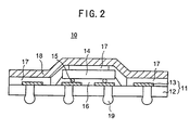
- FIG.2 is a cross-sectional view of a structure of a semiconductor device according to an embodiment of the present invention. -
- the semiconductor device 10 basically comprises a substantially flat interconnection substrate 11 provided as a semiconductor package, a semiconductor element (chip) 14 mounted thereof, a heat radiation plate 18 in the form of a sheet having a concave portion applied to the interconnection substrate 11 so as to cover the semiconductor chip 14, and a solder bump 19 provided as an external connection terminal of the semiconductor device 10.
- the interconnection substrate 11 comprises an interconnection pattern 13 formed in a predetermined shape on one surface (upper surface in FIG.2 ) of an insulating base 12.
- the solder bump (external connection terminal) 19 is formed on the other surface (under surface in FIG.2 ) of the insulating base 12 so that the solder bump 19 is connected to the interconnection pattern 13 through the insulating base 12.
- the solder bump 19 is used to mount the semiconductor device 10 on a mounting substrate such as a motherboard.
- the interconnection pattern 13 is formed only on one side of the interconnection substrate 11. However, not limited to this example, the interconnection pattern 13 may be formed on each side of the interconnection substrate 11. In this case, it should be noted that, since the interconnection pattern 13 formed on the under side of the interconnection substrate 11 is exposed, a protective coat such as a solder resist needs to be formed to protect outwardly the interconnection pattern 13 on the under side.
- an insulating resin film is used, such as a polyimide resin film or an epoxy resin film, on a surface of which an interconnection pattern made of copper (Cu) is formed.
- a TAB tape comprising the polyimide resin film and a copper (Cu) foil formed on one surface thereof by patterning can be used.
- the semiconductor chip 14 is mounted by flip chip bonding so that an electrode terminal 15 thereof is electrically connected to the interconnection pattern 13 of the interconnection substrate 11.
- ACF bonding which uses an anisotropic conductive film (ACF) 16, is employed as this flip chip bonding.
- ACF 16 a thermosetting resin, such as an epoxy resin film containing electrically conductive particles such as silver (Ag) fillers, is used.
- An adhesive 17 bonds the heat radiation plate 18 to the interconnection substrate 11.
- the adhesive 17 is applied to each of the interconnection substrate 11 on the side of the interconnection pattern 13 and the backside (the opposite side to the electrode terminal 15) of the semiconductor chip 14.
- an insulating material such as a thermosetting resin, or an electrically conductive material such as an Ag paste is used according to each occasion, as mentioned hereinafter.
- a semiconductor chip 14 as thin as possible is used.
- semiconductor chips approximately 50 to 100 ⁇ m thick are provided. Such semiconductor chips can be mounted with certain techniques.
- a semiconductor chip 14 as thin as approximately 50 ⁇ m is used in the present embodiment.
- the semiconductor device 10 is characterized in that the heat radiation plate 18 in the form of a sheet having a concave portion is formed of a heat-resistant, molded resin containing carbon fibers.
- a resin reinforced with carbon fibers as this is referred to as a CFRP (Carbon Fiber Reinforced Plastic) hereinafter.
- the heat radiation plate 18 is formed of an adhesive sheet hardened through heating and pressurizing processes, in which is hardened a semihard adhesive sheet in a B-stage (i.e., a CFRP in the form of a prepreg) formed by impregnating a reinforcing material, such as a PAN-based carbon fiber based on a polyacrylonitrile (PAN) or a pitch-based carbon fiber based on a pitch obtained in distilling such a material as a coal tar, with a thermosetting resin such as an epoxy resin.
- a semihard adhesive sheet in a B-stage i.e., a CFRP in the form of a prepreg
- a CFRP in the form of a prepreg
- a reinforcing material such as a PAN-based carbon fiber based on a polyacrylonitrile (PAN) or a pitch-based carbon fiber based on a pitch obtained in distilling such a material as a coal tar
- This heat radiation plate 18 in the form of a sheet i.e., a CFRP hardened and molded
- FIG.3A and FIG.3B show an example of this.
- FIG.3A is a plan view of a structure of carbon fibers of the CFRP (the heat radiation plate 18).
- FIG.3B is a cross-sectional view of the structure taken along a line III-III in FIG.3A .
- a reinforcing material of the CFRP (the heat radiation plate 18) is formed by weaving carbon fibers so that the carbon fibers extend in directions x and y (i.e., directions parallel to a surface of the interconnection substrate 11), as shown in FIG.3A and FIG.3B .
- a coefficient of thermal conductivity in the directions x and y is 40 to 45 W/m ⁇ K.
- a coefficient of thermal conductivity in a perpendicular direction (direction z) to the directions x and y is merely 1 to 2 W/m ⁇ K.
- the coefficient of thermal conductivity in the directions x and y, in which the carbon fibers extend is relatively large. Therefore, by weaving the carbon fibers so that the carbon fibers extend in the directions x and y as shown in FIG.3A and FIG.3B , the heat radiation plate 18 can function effectively.
- the carbon fibers are woven so that the carbon fibers extend in both of the directions x and y in FIG.3A and FIG.3B
- the carbon fibers may be woven so that the carbon fibers extend in arbitrary directionsin a plane x and y.
- FIG.4 is a cross-sectional view showing steps of a manufacturing method of the semiconductor device 10.
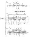
- FIG.5 is a cross-sectional view showing steps succeeding the steps shown in FIG.4 .
- the CFRP 18a is formed, for example, by cutting a CFRP in predetermined length units, as shown by broken lines in FIG.4-(A) , in the course of unrolling a roll of the CFRP (not shown in the figure) rolled up beforehand in a predetermined width and carrying in the unrolled CFRP, as shown by an arrow in FIG.4-(A) .
- the reinforcing material of the CFRP 18a is formed by weaving carbon fibers so that the carbon fibers extend in a plurality of directions parallel to a surface of the interconnection substrate 11, as shown in FIG.3A and FIG.3B .
- the CFRP 18a is molded by using an under mold 21 having a convex shape corresponding to an outline which is to cover the semiconductor chip 14 to be mounted and an upper mold 22 having a concave shape that fits the convex shape of the under mold 21. That is, the CFRP 18a is placed on the under mold 21 and pressurized as shown by an arrow in FIG.4-(B) by using the upper mold 22, while being heated at a temperature of approximately 150°C. Thereby, the CFRP 18a is hardened in a predetermined shape, such as of a cap.
- the CFRP molded as above i.e., the heat radiation plate 18 in the form of a sheet
- the molded heat radiation plate 18 is retrieved from the under mold 21 and the upper mold 22.
- the semiconductor chip 14 is mounted on the substantially flat interconnection substrate 11 having the interconnection pattern 13 formed on one side thereof so that the electrode terminal 15 formed of a gold (Au) bump is electrically connected with the interconnection pattern 13.
- This mounting is performed by using the flip chip bonding. More specifically, the ACF bonding, which uses the anisotropic conductive film (ACF) 16, is employed as this flip chip bonding.
- ACF anisotropic conductive film
- the substantially flat interconnection substrate 11 can be constructed as follows. First, a polyimide resin film (the insulating base 12) having an adhesive layer (not shown in the figure) is prepared. The polyimide resin film is approximately 20 ⁇ m in thickness. Then, a through hole TH is formed at a predetermined portion in the polyimide resin film by laser machining or press working. Next, a copper (Cu) foil approximately 12 ⁇ m thick is applied on the polyimide resin film by thermal press bonding using the adhesive layer. Thereafter, the copper (Cu) foil is formed into the interconnection pattern 13 by photoetching.
- step of mounting the semiconductor chip 14 shown in FIG.4-(C) and the steps of cutting and molding (hardening) the CFRP 18a in the form of a prepreg into the heat radiation plate 18 in the form of a sheet shown in FIG.4-(A) and FIG.4-(B) can be reversed in order.
- the adhesive 17 is applied to each of the interconnection substrate 11 on the side where the interconnection pattern 13 is formed and the backside (the opposite side to the electrode terminal 15) of the semiconductor chip 14.
- an insulating material or an electrically conductive material is used, as mentioned above.
- the structure has to be arranged so that the interconnection pattern 13 for signal use does not short-circuit electrically.
- an electrically conductive adhesive should be used between the backside of the semiconductor chip 14 and the heat radiation plate 18 and also between the interconnection pattern 13 for ground use and the heat radiation plate 18, while an insulating adhesive should be used for other parts.
- the molded CFRP (the heat radiation plate 18 in the form of a sheet) is bonded on the interconnection substrate 11 by using an under mold (comprising a bottom half 23a and a side half 23b) having a concave shape corresponding to an outline of the package and a concave-shaped upper mold 24 which is to be inserted into an opening of the under mold 23a and 23b. That is, the interconnection substrate 11 is placed in the opening of the under mold 23a and 23b so that the side where the adhesive 17 is applied faces upward. Then, the heat radiation plate 18 in the form of a sheet is placed further on the interconnection substrate 11.
- an under mold comprising a bottom half 23a and a side half 23b having a concave shape corresponding to an outline of the package and a concave-shaped upper mold 24 which is to be inserted into an opening of the under mold 23a and 23b. That is, the interconnection substrate 11 is placed in the opening of the under mold 23a and 23b so that the side where the adhesive 17 is applied faces
- the upper mold 24 is used to pressurize the interconnection substrate 11 and the heat radiation plate 18 as shown by an arrow in FIG.5-(B) , while being heated at a temperature of approximately 150°C. Thereby, the molded heat radiation plate 18 in the form of a sheet is bonded on the interconnection substrate 11.
- the interconnection substrate 11 bonded to the heat radiation plate 18 is retrieved from the under mold 23a and 23b and the upper mold 24.
- solder bump (external connection terminal) 19 is formed on the other side of the interconnection substrate 11 (a side opposite to the side to which the heat radiation plate 18 is bonded) so as to be electrically connected with the interconnection pattern 13 of the interconnection substrate 11.
- solder ball approximately 300 ⁇ m in diameter is disposed in the through hole TH formed in the interconnection substrate 11 and then is bonded therein by reflowing. Thereby, the solder ball fills up the through hole TH and is electrically connected to the interconnection pattern 13, forming the solder bump 19 protruding as a ball from the bottom surface of the insulating base 12.
- a conductive membrane be formed on the inner wall of the through hole TH by such a method as copper (Cu) plating, prior to disposing the solder ball in the through hole TH, so as to increase a wettability of the solder.
- Cu copper
- the CFRP in the form of the sheet is used as the heat radiation plate 18 to radiate heat generated from the semiconductor chip 14. Therefore, while the expected heat radiation effect is maintained, the semiconductor device 10 can be miniaturized (thinned down) and lightened, compared to the conventional technology shown in FIG.1C which uses such a material as a metal plate, such as a Cu or Al plate, for heat radiation.
- the carbon fibers of the CFRP are woven so that the carbon fibers extend in the directions x and y (i.e., the directions parallel to a surface of the interconnection substrate 11) in which the coefficient of thermal conductivity is relatively large, the heat can be effectively radiated.
- the CFRP 18a in the form of a prepreg is cut into a predetermined shape
- the CFRP 18a is molded (hardened) through the heating and pressurizing processes into the heat radiation plate 18. Reversing these steps of cutting and molding in order causes inconvenience. That is, if the step of cutting is performed after the step of molding, the cut edge surfaces of the CFRP produce carbon powders so as to taint the CFRP. According to the present embodiment, even if such carbon powders are produced in the step of cutting, the cut edge surfaces of the CFRP 18a are covered with a resin in the following heating process. Thus such an inconvenience is not caused.
- the manufacturing method of the semiconductor device 10 is described as the steps of molding the CFRP 18a in a prepreg form into a predetermined shape (the heat radiation plate 18); and then bonding the heat radiation plate 18 on the interconnection substrate 11 having the semiconductor chip 14 mounted thereon. That is, in this method, the step of molding the CFRP 18a and the step of bonding the heat radiation plate 18 on the interconnection substrate 11 are separated.
- the interconnection substrate 11 is described to be a flexible substrate comprising the insulating resin film, such as a polyimide resin film, and the interconnection pattern of copper (Cu) formed on the surface thereof.
- the interconnection substrate 11 is not limited to this embodiment.
- a rigid substrate such as a glass epoxy resin substrate or a glass BT resin substrate, which is generally used in a build-up multilayer interconnection substrate, may be used as the interconnection substrate 11.
- the interconnection pattern 13 is formed after the through hole TH is formed in the insulating base 12.
- the through hole TH may be formed after the interconnection pattern 13 is formed.
- the solder bump 19 is used as the external connection terminal.
- a material or a form of the external connection terminal is not limited to this embodiment.
- a gold (Au) bump may be substituted for the solder bump 19.
- the external connection terminal may be used in the form of a pin.
- the pin is bonded as follows. First, a proper amount of solder paste is placed at a position, where the external connection terminal is to be formed, of the interconnection pattern 13 exposed from the under side of the insulating base 12 of the interconnection substrate 11. Next, the head portion of the T-shaped pin is placed on the solder paste. Then, the solder paste is hardened by reflowing so as to bond the pin.
Landscapes
- Cooling Or The Like Of Semiconductors Or Solid State Devices (AREA)
- Structures Or Materials For Encapsulating Or Coating Semiconductor Devices Or Solid State Devices (AREA)
Applications Claiming Priority (2)
| Application Number | Priority Date | Filing Date | Title |
|---|---|---|---|
| JP2000014809 | 2000-01-24 | ||
| JP2000014809A JP2001210761A (ja) | 2000-01-24 | 2000-01-24 | 半導体装置及びその製造方法 |
Publications (3)
| Publication Number | Publication Date |
|---|---|
| EP1120830A2 EP1120830A2 (en) | 2001-08-01 |
| EP1120830A3 EP1120830A3 (en) | 2002-05-22 |
| EP1120830B1 true EP1120830B1 (en) | 2009-10-07 |
Family
ID=18542206
Family Applications (1)
| Application Number | Title | Priority Date | Filing Date |
|---|---|---|---|
| EP01300405A Expired - Lifetime EP1120830B1 (en) | 2000-01-24 | 2001-01-18 | Semiconductor device having a carbon fiber reinforced resin as a heat radiation plate with a concave portion |
Country Status (5)
| Country | Link |
|---|---|
| US (2) | US6713863B2 (https=) |
| EP (1) | EP1120830B1 (https=) |
| JP (1) | JP2001210761A (https=) |
| KR (1) | KR20010076329A (https=) |
| DE (1) | DE60140093D1 (https=) |
Families Citing this family (56)
| Publication number | Priority date | Publication date | Assignee | Title |
|---|---|---|---|---|
| JP3446826B2 (ja) * | 2000-04-06 | 2003-09-16 | 沖電気工業株式会社 | 半導体装置及びその製造方法 |
| US6737298B2 (en) * | 2002-01-23 | 2004-05-18 | St Assembly Test Services Ltd | Heat spreader anchoring & grounding method & thermally enhanced PBGA package using the same |
| DE10215654A1 (de) * | 2002-04-09 | 2003-11-06 | Infineon Technologies Ag | Elektronisches Bauteil mit mindestens einem Halbleiterchip und Flip-Chip-Kontakten sowie Verfahren zu seiner Herstellung |
| JP2003309228A (ja) * | 2002-04-18 | 2003-10-31 | Oki Electric Ind Co Ltd | 半導体装置及びその製造方法 |
| US6750552B1 (en) * | 2002-12-18 | 2004-06-15 | Netlogic Microsystems, Inc. | Integrated circuit package with solder bumps |
| TWI233190B (en) * | 2003-02-11 | 2005-05-21 | Via Tech Inc | Structure of chip package and process thereof |
| US7239024B2 (en) * | 2003-04-04 | 2007-07-03 | Thomas Joel Massingill | Semiconductor package with recess for die |
| TWI315094B (en) * | 2003-04-25 | 2009-09-21 | Advanced Semiconductor Eng | Flip chip package |
| JP3786103B2 (ja) * | 2003-05-02 | 2006-06-14 | セイコーエプソン株式会社 | 半導体装置、電子デバイス、電子機器および半導体装置の製造方法 |
| US6821816B1 (en) * | 2003-06-13 | 2004-11-23 | Delphi Technologies, Inc. | Relaxed tolerance flip chip assembly |
| US6875636B2 (en) * | 2003-07-14 | 2005-04-05 | Delphi Technologies, Inc. | Wafer applied thermally conductive interposer |
| TWI376756B (en) * | 2003-07-30 | 2012-11-11 | Taiwan Semiconductor Mfg | Ground arch for wirebond ball grid arrays |
| US7012326B1 (en) | 2003-08-25 | 2006-03-14 | Xilinx, Inc. | Lid and method of employing a lid on an integrated circuit |
| JP3929966B2 (ja) * | 2003-11-25 | 2007-06-13 | 新光電気工業株式会社 | 半導体装置及びその製造方法 |
| JP4641423B2 (ja) | 2004-02-18 | 2011-03-02 | ルネサスエレクトロニクス株式会社 | 半導体装置およびその製造方法 |
| GB2429842B (en) * | 2004-05-20 | 2009-01-28 | Spansion Llc | Method of fabricating semiconductor device and semiconductor device |
| TWI259566B (en) * | 2004-08-31 | 2006-08-01 | Via Tech Inc | Exposed heatsink type semiconductor package and manufacture process thereof |
| TW200636954A (en) * | 2005-04-15 | 2006-10-16 | Siliconware Precision Industries Co Ltd | Thermally enhanced semiconductor package and fabrication method thereof |
| JP4208863B2 (ja) * | 2005-06-30 | 2009-01-14 | 富士通マイクロエレクトロニクス株式会社 | 半導体装置およびその製造方法 |
| KR100824250B1 (ko) * | 2005-08-01 | 2008-04-24 | 엔이씨 일렉트로닉스 가부시키가이샤 | 금속 리드 부재를 피쳐링하는 반도체 패키지 |
| JP2007042719A (ja) * | 2005-08-01 | 2007-02-15 | Nec Electronics Corp | 半導体装置 |
| KR100765478B1 (ko) | 2005-08-12 | 2007-10-09 | 삼성전자주식회사 | 구멍이 형성된 테이프 배선기판과, 그를 이용한 테이프패키지 및 평판 표시 장치 |
| US7388284B1 (en) | 2005-10-14 | 2008-06-17 | Xilinx, Inc. | Integrated circuit package and method of attaching a lid to a substrate of an integrated circuit |
| US7416923B2 (en) * | 2005-12-09 | 2008-08-26 | International Business Machines Corporation | Underfill film having thermally conductive sheet |
| JP2007184351A (ja) | 2006-01-05 | 2007-07-19 | Nec Electronics Corp | 半導体装置及びその製造方法 |
| US20080001277A1 (en) * | 2006-06-30 | 2008-01-03 | Tsrong Yi Wen | Semiconductor package system and method of improving heat dissipation of a semiconductor package |
| JP2008153305A (ja) * | 2006-12-14 | 2008-07-03 | Nec Electronics Corp | 半導体装置 |
| TWI379363B (en) * | 2007-04-24 | 2012-12-11 | United Test & Assembly Ct Lt | Bump on via-packaging and methodologies |
| US7906857B1 (en) | 2008-03-13 | 2011-03-15 | Xilinx, Inc. | Molded integrated circuit package and method of forming a molded integrated circuit package |
| JP2009290118A (ja) * | 2008-05-30 | 2009-12-10 | Toshiba Corp | 電子機器 |
| US20100052156A1 (en) * | 2008-08-27 | 2010-03-04 | Advanced Semiconductor Engineering, Inc. | Chip scale package structure and fabrication method thereof |
| US8097944B2 (en) * | 2009-04-30 | 2012-01-17 | Infineon Technologies Ag | Semiconductor device |
| US8362607B2 (en) * | 2009-06-03 | 2013-01-29 | Honeywell International Inc. | Integrated circuit package including a thermally and electrically conductive package lid |
| US8362609B1 (en) | 2009-10-27 | 2013-01-29 | Xilinx, Inc. | Integrated circuit package and method of forming an integrated circuit package |
| FR2957192B1 (fr) * | 2010-03-03 | 2013-10-25 | Hispano Suiza Sa | Module electronique de puissance pour un actionneur pour aeronef |
| JP5572890B2 (ja) * | 2010-06-08 | 2014-08-20 | ミヨシ電子株式会社 | 半導体モジュールおよび半導体装置 |
| US8810028B1 (en) | 2010-06-30 | 2014-08-19 | Xilinx, Inc. | Integrated circuit packaging devices and methods |
| JP2012033559A (ja) | 2010-07-28 | 2012-02-16 | J Devices:Kk | 半導体装置 |
| JP5955500B2 (ja) * | 2010-10-25 | 2016-07-20 | 稔之 新井 | 放熱構造 |
| US9072199B2 (en) | 2010-12-27 | 2015-06-30 | Src, Inc. | Thermal transfer component, apparatus and method including thermally conductive frame penetrated by thermally conductive plug |
| JP2012164846A (ja) * | 2011-02-08 | 2012-08-30 | Renesas Electronics Corp | 半導体装置、半導体装置の製造方法、及び表示装置 |
| US10109591B1 (en) * | 2011-06-27 | 2018-10-23 | Amkor Technology, Inc. | Integrated shield package and method |
| JP6119950B2 (ja) * | 2011-12-02 | 2017-04-26 | ナガセケムテックス株式会社 | 中空構造電子部品 |
| JP5987358B2 (ja) * | 2012-03-01 | 2016-09-07 | 株式会社ソシオネクスト | 半導体装置及び半導体装置の製造方法 |
| JP6008582B2 (ja) * | 2012-05-28 | 2016-10-19 | 新光電気工業株式会社 | 半導体パッケージ、放熱板及びその製造方法 |
| KR101989516B1 (ko) | 2012-09-24 | 2019-06-14 | 삼성전자주식회사 | 반도체 패키지 |
| CN104576568A (zh) * | 2013-10-15 | 2015-04-29 | 日月光半导体制造股份有限公司 | 半导体封装件及其制造方法 |
| US9559064B2 (en) * | 2013-12-04 | 2017-01-31 | Taiwan Semiconductor Manufacturing Company, Ltd. | Warpage control in package-on-package structures |
| KR102186203B1 (ko) | 2014-01-23 | 2020-12-04 | 삼성전자주식회사 | 패키지 온 패키지 장치 및 이의 제조 방법 |
| JP2016092300A (ja) * | 2014-11-07 | 2016-05-23 | 新光電気工業株式会社 | 半導体装置及び半導体装置の製造方法 |
| FR3053526B1 (fr) | 2016-07-01 | 2018-11-16 | Commissariat A L'energie Atomique Et Aux Energies Alternatives | Procede de fabrication collective de dispositifs electroniques et dispositif electronique |
| FR3079068B1 (fr) * | 2018-03-13 | 2023-05-26 | St Microelectronics Grenoble 2 | Dispositifs electroniques et procedes de fabrication |
| JP7265321B2 (ja) * | 2018-06-21 | 2023-04-26 | デクセリアルズ株式会社 | 半導体装置及び半導体装置の製造方法 |
| EP3719841B1 (en) * | 2019-04-01 | 2022-02-16 | Detection Technology Oy | Radiation sensor element and method |
| CN115181505B (zh) * | 2022-07-12 | 2024-02-27 | 东莞市兆科电子材料科技有限公司 | 导热垫片及其制备方法 |
| WO2025094923A1 (ja) * | 2023-11-02 | 2025-05-08 | ローム株式会社 | 半導体装置 |
Family Cites Families (17)
| Publication number | Priority date | Publication date | Assignee | Title |
|---|---|---|---|---|
| US5476716A (en) * | 1988-10-17 | 1995-12-19 | The Dexter Corporation | Flame retardant epoxy molding compound, method and encapsulated device |
| JPH05209157A (ja) | 1992-01-29 | 1993-08-20 | Nec Corp | 電子デバイス用接着剤 |
| US5523260A (en) | 1993-08-02 | 1996-06-04 | Motorola, Inc. | Method for heatsinking a controlled collapse chip connection device |
| US6347037B2 (en) * | 1994-04-28 | 2002-02-12 | Fujitsu Limited | Semiconductor device and method of forming the same |
| US5415906A (en) * | 1994-05-18 | 1995-05-16 | Denki Kagaku Kogyo Kabushiki Kaisha | Heat resistant electrically conductive plastic sheet and container |
| US5873973A (en) * | 1995-04-13 | 1999-02-23 | Northrop Grumman Corporation | Method for single filament transverse reinforcement in composite prepreg material |
| USH1699H (en) | 1995-10-31 | 1997-12-02 | The United States Of America As Represented By The Secretary Of The Navy | Thermal bond system |
| US5834337A (en) | 1996-03-21 | 1998-11-10 | Bryte Technologies, Inc. | Integrated circuit heat transfer element and method |
| JP3097644B2 (ja) * | 1998-01-06 | 2000-10-10 | 日本電気株式会社 | 半導体装置接続構造及び接続方法 |
| CN1236982A (zh) * | 1998-01-22 | 1999-12-01 | 株式会社日立制作所 | 压力接触型半导体器件及其转换器 |
| JP2000012749A (ja) | 1998-06-24 | 2000-01-14 | Sumitomo Metal Mining Co Ltd | 半導体パッケージ用放熱板 |
| US6093961A (en) * | 1999-02-24 | 2000-07-25 | Chip Coolers, Inc. | Heat sink assembly manufactured of thermally conductive polymer material with insert molded metal attachment |
| US6215180B1 (en) * | 1999-03-17 | 2001-04-10 | First International Computer Inc. | Dual-sided heat dissipating structure for integrated circuit package |
| JP2000281802A (ja) * | 1999-03-30 | 2000-10-10 | Polymatech Co Ltd | 熱伝導性成形体およびその製造方法ならびに半導体装置 |
| US6288900B1 (en) * | 1999-12-02 | 2001-09-11 | International Business Machines Corporation | Warpage compensating heat spreader |
| US6727422B2 (en) * | 2000-09-18 | 2004-04-27 | Chris Macris | Heat sink/heat spreader structures and methods of manufacture |
| US6512295B2 (en) * | 2001-03-01 | 2003-01-28 | International Business Machines Corporation | Coupled-cap flip chip BGA package with improved cap design for reduced interfacial stresses |
-
2000
- 2000-01-24 JP JP2000014809A patent/JP2001210761A/ja active Pending
-
2001
- 2001-01-12 US US09/760,396 patent/US6713863B2/en not_active Expired - Lifetime
- 2001-01-18 KR KR1020010002822A patent/KR20010076329A/ko not_active Ceased
- 2001-01-18 DE DE60140093T patent/DE60140093D1/de not_active Expired - Lifetime
- 2001-01-18 EP EP01300405A patent/EP1120830B1/en not_active Expired - Lifetime
-
2004
- 2004-02-12 US US10/777,232 patent/US6864120B2/en not_active Expired - Lifetime
Also Published As
| Publication number | Publication date |
|---|---|
| US6713863B2 (en) | 2004-03-30 |
| EP1120830A3 (en) | 2002-05-22 |
| US20010009302A1 (en) | 2001-07-26 |
| US6864120B2 (en) | 2005-03-08 |
| JP2001210761A (ja) | 2001-08-03 |
| DE60140093D1 (de) | 2009-11-19 |
| KR20010076329A (ko) | 2001-08-11 |
| US20040166609A1 (en) | 2004-08-26 |
| EP1120830A2 (en) | 2001-08-01 |
Similar Documents
| Publication | Publication Date | Title |
|---|---|---|
| EP1120830B1 (en) | Semiconductor device having a carbon fiber reinforced resin as a heat radiation plate with a concave portion | |
| JP2981141B2 (ja) | グリッドアレイ・プラスチックパッケージ、およびその製造方法、およびその製造に使用されるプラスチック積層体、およびその製造方法 | |
| KR100533673B1 (ko) | 반도체 장치 및 그 제조 방법, 회로 기판 및 전자 기기 | |
| KR100384260B1 (ko) | 반도체장치 및 그 제조방법 | |
| US6995448B2 (en) | Semiconductor package including passive elements and method of manufacture | |
| US5467253A (en) | Semiconductor chip package and method of forming | |
| US8343808B2 (en) | Method of making stackable semiconductor assembly with bump/base/flange heat spreader and build-up circuitry | |
| EP1670057B1 (en) | Manufacturing method of chip integrated substrate | |
| US6475327B2 (en) | Attachment of a stiff heat spreader for fabricating a cavity down plastic chip carrier | |
| US20120126401A1 (en) | Stackable semiconductor assembly with bump/base/flange heat spreader and electromagnetic shielding | |
| US20080067666A1 (en) | Circuit board structure with embedded semiconductor chip and method for fabricating the same | |
| US20050023030A1 (en) | Printed circuit board with a heat dissipation element and package comprising the printed circuit board | |
| US6365979B1 (en) | Semiconductor device and manufacturing method thereof | |
| JP2007503713A (ja) | 電子モジュールおよびその製造方法 | |
| US20080006936A1 (en) | Superfine-circuit semiconductor package structure | |
| US20020062946A1 (en) | Heat radiation fin using a carbon fiber reinforced resin as heat radiation plates standing on a substrate | |
| JP3946659B2 (ja) | 高放熱型プラスチックパッケージ及びその製造方法 | |
| US20020124955A1 (en) | Attachment of a heat spreader for fabricating a cavity down plastic chip carrier | |
| EP0810654A1 (en) | Ball grid array package with substrate having no through holes or via interconnections | |
| US20040262746A1 (en) | High-density chip scale package and method of manufacturing the same | |
| EP1369919A1 (en) | Flip chip package | |
| KR20030085449A (ko) | 개량된 플립 칩 패키지 | |
| KR100401018B1 (ko) | 반도체패키지를 위한 웨이퍼의 상호 접착 방법 | |
| KR100696050B1 (ko) | 캐비티 다운 플라스틱 칩 캐리어를 제조하기 위한 단단한열 확산기의 부착 방법 | |
| EP1365450A1 (en) | An improved wire-bonded chip on board package |
Legal Events
| Date | Code | Title | Description |
|---|---|---|---|
| PUAI | Public reference made under article 153(3) epc to a published international application that has entered the european phase |
Free format text: ORIGINAL CODE: 0009012 |
|
| AK | Designated contracting states |
Kind code of ref document: A2 Designated state(s): AT BE CH CY DE DK ES FI FR GB GR IE IT LI LU MC NL PT SE TR |
|
| AX | Request for extension of the european patent |
Free format text: AL;LT;LV;MK;RO;SI |
|
| PUAL | Search report despatched |
Free format text: ORIGINAL CODE: 0009013 |
|
| AX | Request for extension of the european patent |
Free format text: AL;LT;LV;MK;RO;SI |
|
| 17P | Request for examination filed |
Effective date: 20020611 |
|
| AKX | Designation fees paid |
Designated state(s): DE |
|
| 17Q | First examination report despatched |
Effective date: 20050622 |
|
| 17Q | First examination report despatched |
Effective date: 20050622 |
|
| GRAP | Despatch of communication of intention to grant a patent |
Free format text: ORIGINAL CODE: EPIDOSNIGR1 |
|
| GRAS | Grant fee paid |
Free format text: ORIGINAL CODE: EPIDOSNIGR3 |
|
| GRAA | (expected) grant |
Free format text: ORIGINAL CODE: 0009210 |
|
| AK | Designated contracting states |
Kind code of ref document: B1 Designated state(s): DE |
|
| REF | Corresponds to: |
Ref document number: 60140093 Country of ref document: DE Date of ref document: 20091119 Kind code of ref document: P |
|
| PLBE | No opposition filed within time limit |
Free format text: ORIGINAL CODE: 0009261 |
|
| STAA | Information on the status of an ep patent application or granted ep patent |
Free format text: STATUS: NO OPPOSITION FILED WITHIN TIME LIMIT |
|
| 26N | No opposition filed |
Effective date: 20100708 |
|
| PGFP | Annual fee paid to national office [announced via postgrant information from national office to epo] |
Ref country code: DE Payment date: 20150113 Year of fee payment: 15 |
|
| REG | Reference to a national code |
Ref country code: DE Ref legal event code: R119 Ref document number: 60140093 Country of ref document: DE |
|
| PG25 | Lapsed in a contracting state [announced via postgrant information from national office to epo] |
Ref country code: DE Free format text: LAPSE BECAUSE OF NON-PAYMENT OF DUE FEES Effective date: 20160802 |