EP1111508B1 - Integrierte Schaltung mit Kalibriermitteln zur Kalibrierung eines elektronischen Moduls und Verfahren zum Kalibrieren eines elektronischen Moduls in einer Integrierten Schaltung - Google Patents
Integrierte Schaltung mit Kalibriermitteln zur Kalibrierung eines elektronischen Moduls und Verfahren zum Kalibrieren eines elektronischen Moduls in einer Integrierten Schaltung Download PDFInfo
- Publication number
- EP1111508B1 EP1111508B1 EP99125741A EP99125741A EP1111508B1 EP 1111508 B1 EP1111508 B1 EP 1111508B1 EP 99125741 A EP99125741 A EP 99125741A EP 99125741 A EP99125741 A EP 99125741A EP 1111508 B1 EP1111508 B1 EP 1111508B1
- Authority
- EP
- European Patent Office
- Prior art keywords
- calibrating
- module
- signal
- integrated circuit
- integrated
- Prior art date
- Legal status (The legal status is an assumption and is not a legal conclusion. Google has not performed a legal analysis and makes no representation as to the accuracy of the status listed.)
- Expired - Lifetime
Links
Images



Classifications
-
- G—PHYSICS
- G06—COMPUTING OR CALCULATING; COUNTING
- G06F—ELECTRIC DIGITAL DATA PROCESSING
- G06F11/00—Error detection; Error correction; Monitoring
- G06F11/006—Identification
-
- G—PHYSICS
- G01—MEASURING; TESTING
- G01R—MEASURING ELECTRIC VARIABLES; MEASURING MAGNETIC VARIABLES
- G01R31/00—Arrangements for testing electric properties; Arrangements for locating electric faults; Arrangements for electrical testing characterised by what is being tested not provided for elsewhere
- G01R31/28—Testing of electronic circuits, e.g. by signal tracer
- G01R31/317—Testing of digital circuits
- G01R31/31702—Testing digital circuits including elements other than semiconductor transistors, e.g. biochips, nanofabrics, mems, chips with magnetic elements
Definitions
- the invention relates to an integrated circuit provided with calibration means. at least one electronic module, a method for calibrating in the test phase at least one electronic module of such integrated circuits, as well as a integrated circuit board provided with calibration means.
- the integrated circuits on semiconductor wafers or substrates are commonly tested by a point card test device.
- Several batches of platelets are for example put on hold in the programmed device before the platelets are seized and each placed on a test stand in order to receive the test needles on the corresponding areas of the circuits integrated to test.
- said circuits on the board or substrate are tested one after the other thanks to a tip card resting on the contact pads of one of the circuits to be tested.
- Facilities for testing integrated circuits of a semiconductor substrate may consist of providing metal tracks in sawing strips of the substrate separating each integrated circuit, to connect signal input or output ranges of multiple circuits.
- the connection of several integrated circuits thanks to these metal tracks allows to operate some circuit tests individually or jointly.
- US Patent 5,648,661 describes such an arrangement of metal tracks in saw bands to facilitate testing of multiple integrated circuits on the same substrate or wafer without requiring the use of complicated tips, which saves test time. Tracks metal disappear after sawing the insert to separate each integrated circuit. Note that no means of calibrating modules electronic circuits are not planned and only the realization of said metal tracks normally requires an additional step in the realization of integrated circuits, which is a drawback.
- US Patent 4,928,278 describes a test system for an integrated circuit in order to be able to test various functions of said circuit. For this, the system automatically calibrate synchronization errors of several electronic units providing test signals in parallel to the integrated circuit tested. In this document, the calibration does not concern electronic modules of the integrated circuit, but only of the test, which complicates the circuit testing infrastructure.
- Document US-A-5 790 469 discloses a device and a method for calibrating a voltage generator comprising all the characteristics which are defined in the preamble to the proposed independent claims.
- An object which the object of the invention proposes to resolve consists of a integrated circuit provided with means for calibrating at least one module reference electronics so that the output signal from said module is calibrated precisely to overcome the drawbacks described above.
- Another object which the object of the invention proposes to resolve consists in in a calibration process during the test phase of at least one module electronic integrated circuits so that the output signal of said module is calibrated precisely to overcome the drawbacks described above.
- a integrated circuit board which is characterized in that said circuits integrated are arranged on the board according to the location of their signal input and output ranges to allow needles of a tip card of a power testing machine to land on the ranges of a group of integrated circuits to be able to test and calibrate all the circuits of the group at the same time.
- An advantage of the integrated circuit is that it is able to operate in a manner autonomous calibration of an internal reference signal of a module built-in reference, such as a reference voltage, a time base or a reference frequency, based on an imposed external reference signal and wish. As soon as the calibration phase is finished, a calibration word specific, forming the final calibration parameters, is saved in an internal memory, for example an EEPROM memory, as well as the signature associated.
- a module built-in reference such as a reference voltage, a time base or a reference frequency
- This final calibration memorization prevents each time the power is turned on. subsequent circuit voltage, it is necessary to undertake a new calibration operation and that another external reference signal can allow another unwanted calibration of the reference modules.
- a control is therefore operated to find out if there is a signature stored in said memory. In if so, no calibration procedure is launched, because the word Memory calibration is applied directly to the reference module.
- Another advantage is that groups of integrated circuits of the same plate can be calibrated successively so autonomous using an external reference signal applied at the same time to a group of circuits in the test phase.
- other tests on circuits can be undertaken in addition to the module calibration steps as a group or individually.
- a card with points posed on a group of neighboring integrated circuits allows to supply electric voltage to each circuit of the group and bring in one single operation the reference signal on the corresponding input range of each circuit so that it can calibrate independently.
- Said reference modules are for example a voltage module to supply most of the electronic components of a analog and / or digital part of said circuit at a certain voltage which can be of the order of 2V for example, an oscillator module used to provide a reference frequency or also a time base for the synchronization of different electronic blocks of said circuit.
- the circuit calibration means are arranged to calibrate automatically either reference module. This calibration is normally carried out from successively, but it could also be done in parallel.
- Integrated circuits are usually produced on wafers silicon. After the manufacturing steps of said integrated circuits, it is necessary to subject them to a connection functionality test internal electrical components or electronic components or blocks. For this, the platelets are brought in batches in a test apparatus so that each insert can be automatically entered and placed on a support test. The needles of a spiked card come to rest on the beaches metal signal input and output from each integrated circuit to test them.
- the invention proposes to practice a calibration of certain reference modules in each circuit integrated. This calibration will be carried out independently by the circuit (s) integrated with electric voltage supplying them at the same time external reference signal.
- connection of several circuits to a common substrate is made for example using a multi-point card during the test.
- the location of the signal input and output areas is essential to provide to allow the needles of such a point card to land on beaches of several circuits.
- Integrated circuits are calibrated so during the circuit test, because it facilitates all operations for testing and calibrating said wafers.
- the reference signal 3 in this first form of execution is a reference voltage Vref ext, but of course, it could be a time base signal or a frequency signal reference which will be explained with reference to FIG. 2.
- This voltage of external reference 3 is connected to the two signal input ranges 2 of each circuit 1.
- the integrated circuits 1 of this first embodiment include means for calibrating at least one reference module integrated, that is to say the reference voltage module 9.
- the means of calibration consist of a microcontroller well known to those skilled in the art job.
- This reference voltage module 9 makes it possible to supply for example at a regulated voltage of low value most of the components electronics of said circuit which have not been illustrated for simplification.
- the electrical parameters of each part of the integrated circuits is within a variation margin due to process and are therefore not precisely defined.
- Calibration means allow to overcome this variation of electrical parameters by calibrating each reference module thanks to an external reference signal.
- the means for calibrating the integrated circuits 1, that is to say the microcontroller, include comparison means, such as comparator 4 in this embodiment receiving at its inputs the external reference voltage Ext ref brought to input range 2 and the reference voltage Vref int supplied by the reference voltage module 9, the output 5 of comparator 4 providing a control signal to a microprocessor 6 which manages the whole calibration procedure of the module reference voltage 9, a ROM memory 7 containing an algorithm known to calculation of calibration parameters and being linked to microprocessor 6 for it allow calculation of calibration parameters to be imposed on the module reference voltage 9 as a function of the result of the comparison of the comparator 4, an EEPROM memory 10 connected to the microprocessor 6 and intended to save the final calibration parameters 12 with a signature 11 associated.
- the calibration parameters calculated by the microprocessor 6 using the appropriate algorithm recorded in the ROM memory 7 are transmitted in a calibration register 8 arranged in as an interface in front of the reference voltage module 9. The parameters or the calibration word are addressed in parallel in the register.
- the calibration operation is carried out by iteration until the reference voltage module 9 provides a reference voltage at output Vref int which is equal to the desired external reference voltage Vref ext.
- the calculation algorithm which is known to those skilled in the art can be a linear approach or successive approximation algorithm, for example by dichotomy.
- the comparator output provides information to microprocessor 6 indicating that the calibration is complete.
- the final calibration parameters that is to say the word calibration, are introduced by the microprocessor 6 normally permanently in a 12 portion of memory EEPROM 10 with an associated signature 11 which specifies to the circuit that the calibration operation of the corresponding reference module has been executed.
- TRIM designates a calibration word or calibration parameters of a reference module
- GIS designates the signature associated with said calibration parameters of said module.
- the calibration of the reference voltage module 9 can be carried out by example by modifying resistance values of a resistance network placed in series or in parallel acting on the value of the voltage of reference at the output of said module.
- Another way to calibrate this voltage reference consists in addressing a binary word to a series of switches whose the opening or closing of each switch is controlled by a bit of the binary word, each switch connecting a resistor to a source of specific current.
- This calibration operation also known as English term trimming, will not be more fully described, because it makes part of the knowledge of a person skilled in the art in this field of electronics.
- circuits are separated from each other by a sawing operation of the platelets. Said circuits, thereafter, are mounted on assemblies or are encapsulated.
- any subsequent energization of the integrated circuit no longer entails calibration of reference modules by checking the registered signature in said memory 10. Each time the circuit is energized, the EEPROM 10 memory provides the final calibration parameters by through microprocessor 6 to register 8 so that the reference voltage 9 produces a calibrated reference voltage.
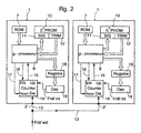
- Figure 2 shows a second embodiment for the calibration of two integrated circuits 1 supplied in parallel by a source of electrical voltage and the same reference signal 13 applied to the ranges input 2 'of each circuit.
- the microprocessor 6, the ROM memory 7 and the EEPROM memory 10 are equivalent to the first embodiment and does not will be described in more detail in greater detail.
- the first form of execution with reference to FIG. 1 only two integrated circuits 1 are shown, but it is clear that several circuits could be connected in parallel with the same reference signal 13 applied to their 2 'input range so that they calibrate independently.
- the reference module to calibrate is an oscillator 19 which outputs a signal with a frequency of reference Fréf int used in particular for the synchronization of different electronic components or logic blocks of said circuit.
- This signal to reference frequency Fref int can be introduced into dividers to define time bases, in particular for the case where the integrated circuit is used in the watchmaking field.
- the external reference frequency signal Fréf ext received on the tracks input 2 ' is brought to one of the inputs of a counter 14, the other of which input receives the signal at internal frequency Fr int from oscillator module 19.
- the counter 14 is initially reset to zero by an erase signal 17 provided by the microprocessor 6.
- a window for reading the two signals to reference frequency is imposed by the microprocessor which provides a read signal 16 to counter 14.
- the result of the difference counter between the two frequencies is an information signal 15 for the microprocessor so that it can calculate calibration parameters using to the memory algorithm 7.
- the calibration parameters which are binary words for example, are transmitted in a register 18 placed at the input of oscillator 19.
- the integrated circuits include a module as well of reference voltage and an oscillator module
- the calibration of each of these modules are operated normally in succession.
- the final parameters calibration of each of these reference modules with the signature associated are placed in different portions of the EEPROM memory.
- Figures 3 and 4 are a representation of how are tested and calibrated several integrated circuits 1 in parallel using a card multiple points.
- the needles 20 of the spiked card are placed on signal input and output ranges 22 of four integrated circuits 1.
- Good of course, more than four integrated circuits 1 could be connected in parallel according to the location of their signal input and output ranges 22.
- the source of electrical voltage for the supply of integrated circuits is connected to two of said pads 22, but is not illustrated so as not to by overloading the figures. This multiple connection of integrated circuits allows parallel integrated circuits to perform calibration independently of their reference modules, but also of ability to group certain functional tests in order to save test time.
- the needles 20 of a multi-point card arise on tracks 22 of four integrated circuits 1 of which two circuits are arranged above the other two circuits.
- the tracks 22 of each circuit must be arranged in such a way that the needles 20 of the spiked card can easily come to rest on said ranges 22.
- each circuit integrated into ranges 22 rotated ⁇ 90 ° from its immediate neighbor.
- the integrated circuit located at the top right has areas of 22 turns of + 90 ° with respect to the integrated circuit located at the top left, while the circuit integrated arranged in bottom on the left has ranges 22 turned from -90 ° by report to the circuit located at the top left.
- This set of four circuits thus integrated into all of the ranges 22 arranged at the periphery of the assembly so to facilitate the creation of a standard point card connecting four integrated circuits for multiple test and calibration.
- a needle 21 of the spiked card arises in particular on the beach input 2 or 2 'described above.
- Each needle on the point card bends upon contact with a corresponding range of one of the circuits. It is therefore necessary that the needles do not overlap in the realization of such cards to avoid short-circuiting them.
- each stage of the manufacturing process is also provided so that each integrated circuit of a group of four integrated circuits be rotated ⁇ 90 ° relative to its neighbor immediate
- the shape of each circuit should be square so as not to waste space on the wafer.
- the external reference signal 3 in this figure 3 represents the voltage of external reference Vref ext which is applied by needles 21 on the input ranges 2.
- Vref ext the voltage of external reference
- the needles 20 of the point card are raised and moved in the direction H to come to rest on four others integrated circuits to be tested and calibrated.
- the location of the needles on the four other circuits are shown in broken lines.
- the needles 20 of a multi-point card arise on the pads 22 of four integrated circuits 1 arranged in line. Each integrated circuit has all the input and output pads 22 arranged along it from two opposite edges. In this configuration, the creation of a tips intended to connect at least four integrated circuits is facilitated. Even if only four integrated circuits are represented in this figure 4 to be tested and calibrated in parallel, it is obvious that the design of a spiked card, for example on 8 circuits integrated arranged online would not pose any real difficulties additional with the possible exception of aligning the needles lay on a larger number of tracks.
- the needles 20 of the spiked card are raised and moved in direction H to come to land on four other circuits integrated to test and calibrate, as explained above.
- the location of needles 20 in this other position is shown in broken lines.
- Figure 5 illustrates the control procedure and for calibrating integrated circuits.
- the integrated circuit is energized 30 whether it is for a circuit in the test phase of a circuit board or for a circuit separated from the plate.
- a power source is connected on two metal areas of the integrated circuit.
- EEPROM memory includes the registered calibration word (s) and a signature associated with each calibration word of a corresponding reference module.
- a calibration operation 32 can take place.
- At least one external reference signal for example Ext ref and / or Fréf ext, is introduced by a metal circuit entry area for that the calibration of the reference module (s) can be done.
- the final calibration parameters i.e. the word of calibration, are saved in EEPROM memory 33 with the signature associated.
- Each calibration word with its signature corresponds to calibration parameters of one of the reference modules.
- the final calibration parameters are placed in register 34 so that the reference module is calibrated 35.
Landscapes
- Engineering & Computer Science (AREA)
- Theoretical Computer Science (AREA)
- Quality & Reliability (AREA)
- Physics & Mathematics (AREA)
- General Engineering & Computer Science (AREA)
- General Physics & Mathematics (AREA)
- Semiconductor Integrated Circuits (AREA)
- Tests Of Electronic Circuits (AREA)
- Testing Or Measuring Of Semiconductors Or The Like (AREA)
Claims (14)
- Integrierte Schaltung (1), die mit Mitteln zum Kalibrieren wenigstens eines elektronischen Moduls während einer Testphase versehen ist, wobei die Kalibrierungsmittel dazu vorgesehen sind, in selbständiger Weise wenigstens ein integriertes elektronisches Referenzmodul (9, 19) in Abhängigkeit von einem externen Referenzsignal (3, 13), das in die Schaltung über eine Eingangsanschlußfläche (2, 2') der Schaltung eingegeben wird, zu kalibrieren und Endparameter der Kalibrierung aufzuzeichnen, dadurch gekennzeichnet, daß die Endparameter der Kalibrierung mit einer zugeordneten Signatur aufgezeichnet werden, wenn das Ausgangssignal des Referenzmoduls gleich dem externen Referenzsignal (3, 13) ist, wobei das Vorhandensein der Signatur ermöglicht, beim Anlegen der Spannung an die integrierte Schaltung die aufgezeichneten Kalibrierungsparameter an das integrierte Referenzmodul (9, 19) zu übertragen, wobei eine Kalibrierungsoperation auch bei Abwesenheit der Signatur stattfinden kann.
- Integrierte Schaltung nach Anspruch 1, dadurch gekennzeichnet, daß die Kalibrierungsmittel Vergleichsmittel (4, 14), die dazu vorgesehen sind, am Eingang das Ausgangssignal des Referenzmoduls (9, 19) und das externe Referenzsignal (3, 13) zu empfangen und am Ausgang ein Vergleichssignal zu liefern, einen Mikroprozessor (6), der die Kalibrierung des Referenzmoduls (9, 19) in Abhängigkeit von dem empfangenen Vergleichssignal der Vergleichsmittel (4, 14) steuert, einen ersten Speicher (7), der einen Rechenalgorithmus enthält und mit dem Mikroprozessor (6) verbunden ist, um diesem zu ermöglichen, Kalibrierungsparameter in Abhängigkeit von dem Vergleichssignal zu berechnen, und einen zweiten Speicher (10), der mit dem Mikroprozessor (6) verbunden ist, um die Endparameter (12) der Kalibrierung des Moduls sowie eine den Parametern zugeordnete Signatur (11) aufzuzeichnen, umfassen.
- Integrierte Schaltung nach Anspruch 2, dadurch gekennzeichnet, daß das Referenzmodul (9, 19) am Ausgang eine Referenzspannung (Vref int) liefert und daß die Vergleichsmittel ein Komparator (4) sind, dessen zwei Eingänge die Referenzspannung (Vref int) des zu kalibrierenden Moduls und eine externe Referenzspannung (Vref ext) empfangen.
- Integrierte Schaltung nach Anspruch 2, dadurch gekennzeichnet, daß das Referenzmodul ein Oszillator (19) ist, der am Ausgang ein Signal mit Referenzfrequenz (Fref int) liefert, und daß die Vergleichsmittel ein Zähler (14) sind, dessen zwei Eingänge das Signal mit Referenzfrequenz (Fref int) des Oszillators (19) und das Signal mit externer Referenzfrequenz (Fref ext) empfangen.
- Integrierte Schaltung nach einem der vorhergehenden Ansprüche, dadurch gekennzeichnet, daß sie ein erstes Referenzmodul (9), das am Ausgang eine Referenzspannung (Vref int) liefert, und ein zweites Referenzmodul (19), das am Ausgang ein Signal mit Referenzfrequenz (Fref int) liefert, umfaßt, daß die Schaltung an einer ersten Eingangsanschlußfläche (2) eine externe Referenzspannung (Vref ext) empfängt, um das erste Referenzmodul (9) zu kalibrieren, und an einer zweiten Eingangsanschlußfläche (2) ein Signal mit externer Referenzfrequenz (Fref ext) empfängt, um das zweite Referenzmodul (19) zu kalibrieren.
- Integrierte Schaltung nach Anspruch 1, dadurch gekennzeichnet, daß das Referenzmodul am Ausgang ein Taktsignal liefert, das in den Vergleichsmitteln der Kalibrierungsmittel mit einem externen Taktsignal verglichen wird.
- Integrierte Schaltung nach Anspruch 2, dadurch gekennzeichnet, daß der erste Speicher ein ROM-Speicher (7) ist, daß der zweite Speicher ein EEPROM-Speicher (10) ist und daß ein Datenregister (8, 18) als Schnittstelle am Eingang des Referenzmoduls angeordnet ist, um die Kalibrierungsparameter zu empfangen.
- Verfahren zum Kalibrieren wenigstens eines integrierten elektronischen Referenzmoduls (9, 19) wenigstens einer integrierten Schaltung (1) nach einem der vorhergehenden Ansprüche während einer Testphase, das die folgenden Schritte umfaßt:a) Versorgen der integrierten Schaltung (1) mit einer externen Quelle für elektrische Spannung,b) Eingeben eines externen Referenzsignals (3, 13) in eine der Eingangsanschlußflächen (2, 2') der integrierten Schaltung in Verbindung mit den Kalibrierungsmitteln der integrierten Schaltung (1), damit sie in selbständiger Weise durch Iteration das elektronische Referenzmodul (9, 19) mit Hilfe von Kalibrierungsparametern kalibrieren, bis das Referenzausgangssignal des Referenzmoduls gleich dem externen Referenzsignal (3, 13) ist, undc) Aufzeichnen der Endparameter (12) der Kalibrierung, die von den Kalibrierungsmitteln geliefert werden, dadurch gekennzeichnet, daß die Endparameter der Kalibrierung sowie eine den Parametern zugeordnete Signatur (11) in Speichermitteln (10) aufgezeichnet werden, wobei das Vorhandensein der Signatur ermöglicht, beim Anlegen der Spannung an die integrierte Schaltung die aufgezeichneten Kalibrierungsparameter an das integrierte Referenzmodul (9, 19) zu übertragen, wobei eine Kalibrierungsoperation auch bei Abwesenheit der Signatur stattfinden kann.
- Verfahren nach Anspruch 8, dadurch gekennzeichnet, daß im Schritt b) in den Kalibrierungsmitteln das externe Referenzsignal (3, 13) mit dem Ausgangssignal des Referenzmoduls (9, 19) in den Vergleichsmitteln (4, 14) verglichen wird, daß die Kalibrierungsparameter in einem Mikroprozessor (6) in Abhängigkeit vom Ausgangssignal der Vergleichsmittel (4, 14) und auf der Grundlage eines Rechenalgorithmus eines mit dem Mikroprozessor (6) verbundenen ersten Speichers (7) berechnet werden, daß die Kalibrierungsparameter in das Referenzmodul (9, 19) eingegeben werden, um dessen Referenzausgangssignal zu modifizieren, daß die vorhergehenden Operationen wiederholt werden, bis das Referenzsignal des Moduls gleich dem externen Referenzsignal (3, 13) ist, und daß die Endparameter (12) der Kalibrierung in dauerhafter Weise vom Mikroprozessor (6) in einem zweiten Speicher (10), der den Speichermitteln entspricht, zusammen mit einer den Endparametern zugeordneten Signatur (11) aufgezeichnet werden, damit der zweite Speicher (10) jedesmal, wenn an die Schaltung eine Spannung angelegt wird, automatisch an den Mikroprozessor (6) die Endparameter der Kalibrierung liefert, um sie in das Referenzmodul (9, 19) einzugeben, damit es ein kalibriertes internes Referenzsignal liefert.
- Kalibrierungsverfahren nach einem der Ansprüche 8 und 9, dadurch gekennzeichnet, daß mehrere integrierte Schaltungen (1) auf demselben Halbleitersubstrat mit einer Spannung versorgt werden und sich in selbständiger Weise gleichzeitig mit Hilfe desselben externen Referenzsignals, das während der Testphase an die entsprechende Eingangsanschlußfläche (2, 2') jeder Schaltung angelegt wird, kalibrieren.
- Kalibrierungsverfahren nach Anspruch 10, dadurch gekennzeichnet, daß die Stifte einer Mehrfachspitzen-Karte (20) einer Testmaschine auf den Signaleingangs- und Signalausgangs-Anschlußflächen wenigstens zweier benachbarter integrierter Schaltungen, vorzugsweise auf vier benachbarten integrierten Schaltungen, zu liegen kommen, damit diese sich in selbständiger Weise gleichzeitig kalibrieren.
- Kalibrierungsverfahren nach Anspruch 8, dadurch gekennzeichnet, daß jede integrierte Schaitung ein erstes Referenzmodul (9), das am Ausgang eine Referenzspannung (Vref int) liefert, und ein zweites Referenzmodul (19), das am Ausgang ein Signal mit Referenzfrequenz (Fref int) liefert, umfaßt, daß die Schaltung an einer ersten Eingangsanschlußfläche (2) eine externe Referenzspannung (Vref ext) empfängt, um das erste Referenzmodul (9) zu kalibrieren, und an einer zweiten Eingangsanschlußfläche (2') ein Signal mit externer Referenzfrequenz (Fref ext) empfängt, um das zweite Referenzmodul (19) zu kalibrieren.
- Chip für integrierte Schaltungen nach einem der Ansprüche 1 bis 7, dadurch gekennzeichnet, daß die integrierten Schaltungen (1) auf dem Chip in Gruppen benachbarter und ähnlicher Schaltungen angeordnet sind, die unterschiedliche Orientierungen besitzen, derart, daß der Ort ihrer Signaleingangs- und Signalausgangs-Anschlußflächen (22) den Stiften (21) einer Karte mit Spitzen einer Testmaschine ermöglicht, auf den Anschlußflächen (22) einer der Gruppen aus integrierten Schaltungen (1) zu liegen zu kommen, um sämtliche Schaltungen der Gruppe gleichzeitig testen und kalibrieren zu können.
- Chip nach Anspruch 13, dadurch gekennzeichnet, daß die Gruppe (1) aus integrierten Schaltungen vier benachbarte integrierte Schaltungen umfaßt, deren Schaltungen auf zwei parallelen Linien in der Weise angeordnet sind, daß eine im wesentliche quadratische Gruppe gebildet wird, wobei jede Schaltung in bezug auf ihren direkten Nachbarn um ±90° gedreht ist, so daß sich sämtliche Anschlußflächen (22) am Umfang der Gruppe befinden.
Priority Applications (5)
| Application Number | Priority Date | Filing Date | Title |
|---|---|---|---|
| EP99125741A EP1111508B1 (de) | 1999-12-23 | 1999-12-23 | Integrierte Schaltung mit Kalibriermitteln zur Kalibrierung eines elektronischen Moduls und Verfahren zum Kalibrieren eines elektronischen Moduls in einer Integrierten Schaltung |
| AT99125741T ATE240550T1 (de) | 1999-12-23 | 1999-12-23 | Integrierte schaltung mit kalibriermitteln zur kalibrierung eines elektronischen moduls und verfahren zum kalibrieren eines elektronischen moduls in einer integrierten schaltung |
| DE69907930T DE69907930T2 (de) | 1999-12-23 | 1999-12-23 | Integrierte Schaltung mit Kalibriermitteln zur Kalibrierung eines elektronischen Moduls und Verfahren zum Kalibrieren eines elektronischen Moduls in einer Integrierten Schaltung |
| US09/742,861 US6691055B2 (en) | 1999-12-23 | 2000-12-20 | Integrated circuit provided with means for calibrating an electronic module and method for calibrating an electronic module of an integrated circuit |
| JP2000390048A JP4754686B2 (ja) | 1999-12-23 | 2000-12-22 | 電子モジュールを較正する手段を備える集積回路および集積回路の電子モジュールを較正する方法 |
Applications Claiming Priority (1)
| Application Number | Priority Date | Filing Date | Title |
|---|---|---|---|
| EP99125741A EP1111508B1 (de) | 1999-12-23 | 1999-12-23 | Integrierte Schaltung mit Kalibriermitteln zur Kalibrierung eines elektronischen Moduls und Verfahren zum Kalibrieren eines elektronischen Moduls in einer Integrierten Schaltung |
Publications (2)
| Publication Number | Publication Date |
|---|---|
| EP1111508A1 EP1111508A1 (de) | 2001-06-27 |
| EP1111508B1 true EP1111508B1 (de) | 2003-05-14 |
Family
ID=8239701
Family Applications (1)
| Application Number | Title | Priority Date | Filing Date |
|---|---|---|---|
| EP99125741A Expired - Lifetime EP1111508B1 (de) | 1999-12-23 | 1999-12-23 | Integrierte Schaltung mit Kalibriermitteln zur Kalibrierung eines elektronischen Moduls und Verfahren zum Kalibrieren eines elektronischen Moduls in einer Integrierten Schaltung |
Country Status (5)
| Country | Link |
|---|---|
| US (1) | US6691055B2 (de) |
| EP (1) | EP1111508B1 (de) |
| JP (1) | JP4754686B2 (de) |
| AT (1) | ATE240550T1 (de) |
| DE (1) | DE69907930T2 (de) |
Cited By (1)
| Publication number | Priority date | Publication date | Assignee | Title |
|---|---|---|---|---|
| TWI550285B (zh) * | 2013-12-27 | 2016-09-21 | And a storage device and electronic device for electrically correcting parameters of the wafer |
Families Citing this family (31)
| Publication number | Priority date | Publication date | Assignee | Title |
|---|---|---|---|---|
| JP4124557B2 (ja) * | 2000-10-05 | 2008-07-23 | 松下電器産業株式会社 | 半導体集積回路装置及びその制御方法 |
| JP4278325B2 (ja) * | 2001-12-19 | 2009-06-10 | 株式会社ルネサステクノロジ | 半導体集積回路装置 |
| DE60206149D1 (de) * | 2002-07-05 | 2005-10-20 | St Microelectronics Sa | Verfahren zum Betreiben eines Mikrokontrollerchips mit einem internen RC-Oszillator, und Mikrokontrollerchip zur Durchführung des Verfahrens |
| US7814350B2 (en) * | 2002-10-03 | 2010-10-12 | Via Technologies, Inc. | Microprocessor with improved thermal monitoring and protection mechanism |
| US7770042B2 (en) * | 2002-10-03 | 2010-08-03 | Via Technologies, Inc. | Microprocessor with improved performance during P-state transitions |
| US7774627B2 (en) * | 2002-10-03 | 2010-08-10 | Via Technologies, Inc. | Microprocessor capable of dynamically increasing its performance in response to varying operating temperature |
| US20050006726A1 (en) * | 2003-04-01 | 2005-01-13 | Infineon Technologies Ag | Apparatus and method for testing semiconductor nodules on a semiconductor substrate wafer |
| US20050185769A1 (en) * | 2004-02-25 | 2005-08-25 | Pickerd John J. | Calibration method and apparatus |
| KR100609930B1 (ko) | 2004-07-30 | 2006-08-08 | (주)테라빛 | 검사용 패턴이 형성된 회로기판 및 이를 이용한 메모리카드 제조 방법 |
| US7433790B2 (en) * | 2005-06-06 | 2008-10-07 | Standard Microsystems Corporation | Automatic reference voltage trimming technique |
| US7289924B2 (en) * | 2005-07-20 | 2007-10-30 | Honeywell International Inc. | Self-calibrating sensor |
| US7498891B2 (en) * | 2005-10-18 | 2009-03-03 | Stmicroelectronics Pvt. Ltd. | Method for calibration of an oscillator for a microcontroller chip operation |
| US7460983B2 (en) * | 2006-08-23 | 2008-12-02 | Tektronix, Inc. | Signal analysis system and calibration method |
| US7405575B2 (en) * | 2006-08-23 | 2008-07-29 | Tektronix, Inc. | Signal analysis system and calibration method for measuring the impedance of a device under test |
| US7414411B2 (en) * | 2006-08-23 | 2008-08-19 | Tektronix, Inc. | Signal analysis system and calibration method for multiple signal probes |
| US7408363B2 (en) * | 2006-08-23 | 2008-08-05 | Tektronix, Inc. | Signal analysis system and calibration method for processing acquires signal samples with an arbitrary load |
| US7888955B2 (en) * | 2007-09-25 | 2011-02-15 | Formfactor, Inc. | Method and apparatus for testing devices using serially controlled resources |
| US9588188B1 (en) * | 2008-10-17 | 2017-03-07 | Steril-Aire, Inc. | System and method of monitoring an electronic discharge device in an air purfication system |
| TWI441270B (zh) * | 2008-12-17 | 2014-06-11 | 財團法人工業技術研究院 | 三維積體電路之直通矽晶穿孔製程監控方法及裝置 |
| US8386829B2 (en) * | 2009-06-17 | 2013-02-26 | Macronix International Co., Ltd. | Automatic internal trimming calibration method to compensate process variation |
| EP2363960B1 (de) * | 2010-03-01 | 2012-08-22 | Austriamicrosystems AG | Integrierte Schaltung mit internem RC-Oszillator und Verfahren zur Kalibrierung eines RC-Oszillators |
| JP5472470B2 (ja) * | 2010-08-20 | 2014-04-16 | 富士通株式会社 | 半導体装置 |
| US9041422B2 (en) * | 2011-03-31 | 2015-05-26 | Intel Mobile Communications GmbH | Circuit arrangement with a plurality of on-chip monitor circuits and a control circuit and corresponding methods |
| CN103048530A (zh) * | 2011-10-12 | 2013-04-17 | 鸿富锦精密工业(深圳)有限公司 | 数字电源电流校准装置 |
| KR20170066082A (ko) | 2015-12-04 | 2017-06-14 | 삼성전자주식회사 | Bist 회로, 이를 포함하는 메모리 장치 및 이의 동작방법 |
| US10180486B2 (en) * | 2016-03-16 | 2019-01-15 | Formfactor Beaverton, Inc. | Test standards and methods for impedance calibration of a probe system, and probe systems that include the test standards or utilize the methods |
| DE102018110252A1 (de) * | 2018-04-27 | 2019-10-31 | Infineon Technologies Ag | Transceiver, System mit Transceivern und Signal |
| EP3933638A1 (de) | 2020-06-29 | 2022-01-05 | Siemens Aktiengesellschaft | Konsensusverfahren für eine verteilte datenbank |
| CN113253787A (zh) * | 2021-06-17 | 2021-08-13 | 苏州裕太微电子有限公司 | 一种芯片内电阻校正电路 |
| CN114115427A (zh) * | 2021-11-26 | 2022-03-01 | 中国电子科技集团公司第五十八研究所 | 一种SoC中基于EFLASH加载的LDO校准方法 |
| EP4224178A1 (de) * | 2022-02-03 | 2023-08-09 | Siemens Aktiengesellschaft | Kalibrierung einer elektronischen baugruppe während eines fertigungsprozesses |
Family Cites Families (15)
| Publication number | Priority date | Publication date | Assignee | Title |
|---|---|---|---|---|
| US5070297A (en) * | 1990-06-04 | 1991-12-03 | Texas Instruments Incorporated | Full wafer integrated circuit testing device |
| US5319370A (en) * | 1992-08-31 | 1994-06-07 | Crystal Semiconductor, Inc. | Analog-to-digital converter with a continuously calibrated voltage reference |
| JPH06148279A (ja) * | 1992-10-30 | 1994-05-27 | Yokogawa Hewlett Packard Ltd | 電子デバイス試験・測定装置、およびそのタイミングならびに電圧レベル校正方法 |
| JPH06152549A (ja) * | 1992-11-05 | 1994-05-31 | Fujitsu Ltd | 動作レベル測定装置 |
| JP3098897B2 (ja) * | 1993-07-23 | 2000-10-16 | 三菱電機株式会社 | オフセット調整装置 |
| JPH07113829A (ja) * | 1993-10-18 | 1995-05-02 | Advantest Corp | 時間・周波数測定装置 |
| US5382922A (en) * | 1993-12-23 | 1995-01-17 | International Business Machines Corporation | Calibration systems and methods for setting PLL gain characteristics and center frequency |
| JPH09172143A (ja) * | 1995-12-19 | 1997-06-30 | Mitsubishi Electric Corp | 半導体集積回路装置及びそのテスト方法 |
| JPH09172370A (ja) * | 1995-12-19 | 1997-06-30 | Toshiba Corp | Pll回路 |
| US5699312A (en) * | 1996-04-18 | 1997-12-16 | Altera Corporation | Programmable voltage supply circuitry |
| JPH10260742A (ja) * | 1997-03-19 | 1998-09-29 | Advantest Corp | 精密電圧発生装置 |
| US6064947A (en) * | 1997-08-27 | 2000-05-16 | Texas Instruments Incorporated | Time base generator internal voltage-controlled oscillator calibration system and method |
| JP3842879B2 (ja) * | 1997-10-20 | 2006-11-08 | 松下電器産業株式会社 | ウェハ一括型プローブカードおよび半導体装置の検査方法 |
| US6157198A (en) * | 1998-06-10 | 2000-12-05 | Anritsu Company | Automatic timebase calibration for synchronizing a timebase frequency with a frequency reference standard |
| US6151238A (en) * | 1999-02-23 | 2000-11-21 | Microchip Technology, Inc. | Calibrating functions of an integrated circuit and storing calibration parameters thereof in a programmable fuse array |
-
1999
- 1999-12-23 EP EP99125741A patent/EP1111508B1/de not_active Expired - Lifetime
- 1999-12-23 DE DE69907930T patent/DE69907930T2/de not_active Expired - Lifetime
- 1999-12-23 AT AT99125741T patent/ATE240550T1/de not_active IP Right Cessation
-
2000
- 2000-12-20 US US09/742,861 patent/US6691055B2/en not_active Expired - Lifetime
- 2000-12-22 JP JP2000390048A patent/JP4754686B2/ja not_active Expired - Lifetime
Cited By (1)
| Publication number | Priority date | Publication date | Assignee | Title |
|---|---|---|---|---|
| TWI550285B (zh) * | 2013-12-27 | 2016-09-21 | And a storage device and electronic device for electrically correcting parameters of the wafer |
Also Published As
| Publication number | Publication date |
|---|---|
| US6691055B2 (en) | 2004-02-10 |
| JP2001235517A (ja) | 2001-08-31 |
| ATE240550T1 (de) | 2003-05-15 |
| DE69907930T2 (de) | 2004-05-13 |
| DE69907930D1 (de) | 2003-06-18 |
| EP1111508A1 (de) | 2001-06-27 |
| US20010007091A1 (en) | 2001-07-05 |
| JP4754686B2 (ja) | 2011-08-24 |
Similar Documents
| Publication | Publication Date | Title |
|---|---|---|
| EP1111508A1 (de) | Integrierte Schaltung mit kalibriermitteln zur kalibrierung eines elektronischen Moduls und Verfahren zum kalibrieren eines elektronischen Moduls in einer Integrierten Schaltung | |
| FR2476851A1 (fr) | Procedes et appareils de controle automatique de circuits electriques | |
| EP0318363A1 (de) | Verfahren zum Testen von Zellen von elektrisch programmierbaren Speichern und entsprechende integrierte Schaltung | |
| FR2555331A1 (fr) | Circuit comprenant un micro-ordinateur destine notamment au reglage du siege d'un vehicule automobile | |
| FR2837960A1 (fr) | Entite electronique transactionnelle securisee par mesure du temps | |
| EP0349412A1 (de) | Datenträger und Steuerungssystem dieser Träger | |
| EP0146661A1 (de) | Elektrisches Untersuchungsverfahren zur Identifizierung einer defekten Zelle in einer Kette von Zellen, die ein Schieberegister bilden | |
| EP3545621B1 (de) | Schaltelement für eine leistungsschaltung | |
| EP0696031B1 (de) | Programmierbarer integrierter Speicher mit Emulationseinrichtung | |
| FR2653278A1 (fr) | Horloge synchronisee. | |
| FR2737782A1 (fr) | Systeme electronique testable | |
| WO1999013348A1 (fr) | Procede et dispositif pour determiner l'etat de vieillissement d'un condensateur | |
| TW531656B (en) | Circuit arrangement to burn-in-test the semiconductor module | |
| FR2829265A1 (fr) | Detection d'une variation de l'environnement d'un circuit integre | |
| EP0718850B1 (de) | Verfahren und Schaltung zum Testen von integriertem Speicher | |
| EP1688753B1 (de) | Sicherung des Testmodus eines integrierten Schaltkreises | |
| EP1862785A1 (de) | Elektronischer Schaltkreis mit Anzeige der Zeit und der Temperatur zum Einsetzen in ein Überwachungsprodukt | |
| EP1507270B1 (de) | Gerät zur Prüfung des Alterungsgrades eines Varistors | |
| EP1388809B1 (de) | Elektronische Schaltung mit Mitteln zur Spannungskontrolle | |
| EP1081630B1 (de) | Verfahren zur Datenübertragung zwischen einer Chipkarte und einem Leser im Falle eines ungewollten Stromausfalles | |
| FR2765342A1 (fr) | Procede et dispositif de gestion du fonctionnement sous irradiation d'un composant electronique a transistors mos complementaires | |
| FR3018137A1 (de) | ||
| FR2623630A1 (fr) | Procede et dispositif de localisation des pannes de circuits logiques | |
| BE1005660A6 (fr) | Relation a grande vitesse d'essais en circuit et de fonctionnement de circuits electroniques. | |
| EP0594478B1 (de) | Anwendungsspezifische Integrierte Schaltung mit einem Mikroprozessor und Prüfmitteln |
Legal Events
| Date | Code | Title | Description |
|---|---|---|---|
| PUAI | Public reference made under article 153(3) epc to a published international application that has entered the european phase |
Free format text: ORIGINAL CODE: 0009012 |
|
| AK | Designated contracting states |
Kind code of ref document: A1 Designated state(s): AT BE CH CY DE DK ES FI FR GB GR IE IT LI LU MC NL PT SE |
|
| AX | Request for extension of the european patent |
Free format text: AL;LT;LV;MK;RO;SI |
|
| 17P | Request for examination filed |
Effective date: 20011227 |
|
| AKX | Designation fees paid |
Free format text: AT BE CH CY DE DK ES FI FR GB GR IE IT LI LU MC NL PT SE |
|
| GRAH | Despatch of communication of intention to grant a patent |
Free format text: ORIGINAL CODE: EPIDOS IGRA |
|
| GRAH | Despatch of communication of intention to grant a patent |
Free format text: ORIGINAL CODE: EPIDOS IGRA |
|
| GRAA | (expected) grant |
Free format text: ORIGINAL CODE: 0009210 |
|
| AK | Designated contracting states |
Designated state(s): AT BE CH CY DE DK ES FI FR GB GR IE IT LI LU MC NL PT SE |
|
| PG25 | Lapsed in a contracting state [announced via postgrant information from national office to epo] |
Ref country code: NL Free format text: LAPSE BECAUSE OF FAILURE TO SUBMIT A TRANSLATION OF THE DESCRIPTION OR TO PAY THE FEE WITHIN THE PRESCRIBED TIME-LIMIT Effective date: 20030514 Ref country code: IE Free format text: LAPSE BECAUSE OF NON-PAYMENT OF DUE FEES Effective date: 20030514 Ref country code: FI Free format text: LAPSE BECAUSE OF FAILURE TO SUBMIT A TRANSLATION OF THE DESCRIPTION OR TO PAY THE FEE WITHIN THE PRESCRIBED TIME-LIMIT Effective date: 20030514 Ref country code: AT Free format text: LAPSE BECAUSE OF FAILURE TO SUBMIT A TRANSLATION OF THE DESCRIPTION OR TO PAY THE FEE WITHIN THE PRESCRIBED TIME-LIMIT Effective date: 20030514 |
|
| REG | Reference to a national code |
Ref country code: GB Ref legal event code: FG4D Free format text: NOT ENGLISH |
|
| REG | Reference to a national code |
Ref country code: CH Ref legal event code: EP |
|
| REG | Reference to a national code |
Ref country code: IE Ref legal event code: FG4D Free format text: FRENCH |
|
| REF | Corresponds to: |
Ref document number: 69907930 Country of ref document: DE Date of ref document: 20030618 Kind code of ref document: P |
|
| PG25 | Lapsed in a contracting state [announced via postgrant information from national office to epo] |
Ref country code: SE Free format text: LAPSE BECAUSE OF FAILURE TO SUBMIT A TRANSLATION OF THE DESCRIPTION OR TO PAY THE FEE WITHIN THE PRESCRIBED TIME-LIMIT Effective date: 20030814 Ref country code: PT Free format text: LAPSE BECAUSE OF FAILURE TO SUBMIT A TRANSLATION OF THE DESCRIPTION OR TO PAY THE FEE WITHIN THE PRESCRIBED TIME-LIMIT Effective date: 20030814 Ref country code: GR Free format text: LAPSE BECAUSE OF FAILURE TO SUBMIT A TRANSLATION OF THE DESCRIPTION OR TO PAY THE FEE WITHIN THE PRESCRIBED TIME-LIMIT Effective date: 20030814 Ref country code: DK Free format text: LAPSE BECAUSE OF FAILURE TO SUBMIT A TRANSLATION OF THE DESCRIPTION OR TO PAY THE FEE WITHIN THE PRESCRIBED TIME-LIMIT Effective date: 20030814 |
|
| PG25 | Lapsed in a contracting state [announced via postgrant information from national office to epo] |
Ref country code: ES Free format text: LAPSE BECAUSE OF FAILURE TO SUBMIT A TRANSLATION OF THE DESCRIPTION OR TO PAY THE FEE WITHIN THE PRESCRIBED TIME-LIMIT Effective date: 20030825 |
|
| GBT | Gb: translation of ep patent filed (gb section 77(6)(a)/1977) | ||
| NLV1 | Nl: lapsed or annulled due to failure to fulfill the requirements of art. 29p and 29m of the patents act | ||
| REG | Reference to a national code |
Ref country code: CH Ref legal event code: NV Representative=s name: ICB INGENIEURS CONSEILS EN BREVETS SA |
|
| PG25 | Lapsed in a contracting state [announced via postgrant information from national office to epo] |
Ref country code: LU Free format text: LAPSE BECAUSE OF NON-PAYMENT OF DUE FEES Effective date: 20031223 Ref country code: CY Free format text: LAPSE BECAUSE OF FAILURE TO SUBMIT A TRANSLATION OF THE DESCRIPTION OR TO PAY THE FEE WITHIN THE PRESCRIBED TIME-LIMIT Effective date: 20031223 |
|
| PG25 | Lapsed in a contracting state [announced via postgrant information from national office to epo] |
Ref country code: MC Free format text: LAPSE BECAUSE OF NON-PAYMENT OF DUE FEES Effective date: 20031231 Ref country code: BE Free format text: LAPSE BECAUSE OF NON-PAYMENT OF DUE FEES Effective date: 20031231 |
|
| REG | Reference to a national code |
Ref country code: IE Ref legal event code: FD4D Ref document number: 1111508E Country of ref document: IE |
|
| PLBE | No opposition filed within time limit |
Free format text: ORIGINAL CODE: 0009261 |
|
| STAA | Information on the status of an ep patent application or granted ep patent |
Free format text: STATUS: NO OPPOSITION FILED WITHIN TIME LIMIT |
|
| 26N | No opposition filed |
Effective date: 20040217 |
|
| BERE | Be: lapsed |
Owner name: *ADVANCED TECHNOLOGY MATERIALS INC. Effective date: 20031231 Owner name: S.A. MICROELECTRONIC-MARIN *EM Effective date: 20031231 |
|
| REG | Reference to a national code |
Ref country code: FR Ref legal event code: PLFP Year of fee payment: 17 |
|
| REG | Reference to a national code |
Ref country code: FR Ref legal event code: PLFP Year of fee payment: 18 |
|
| PG25 | Lapsed in a contracting state [announced via postgrant information from national office to epo] |
Ref country code: IT Free format text: LAPSE BECAUSE OF NON-PAYMENT OF DUE FEES Effective date: 20151223 |
|
| PGFP | Annual fee paid to national office [announced via postgrant information from national office to epo] |
Ref country code: GB Payment date: 20161228 Year of fee payment: 18 Ref country code: CH Payment date: 20161227 Year of fee payment: 18 |
|
| PGFP | Annual fee paid to national office [announced via postgrant information from national office to epo] |
Ref country code: FR Payment date: 20161227 Year of fee payment: 18 |
|
| PGFP | Annual fee paid to national office [announced via postgrant information from national office to epo] |
Ref country code: DE Payment date: 20161229 Year of fee payment: 18 |
|
| PG25 | Lapsed in a contracting state [announced via postgrant information from national office to epo] |
Ref country code: IT Free format text: LAPSE BECAUSE OF NON-PAYMENT OF DUE FEES Effective date: 20151223 |
|
| PGFP | Annual fee paid to national office [announced via postgrant information from national office to epo] |
Ref country code: IT Payment date: 20161222 Year of fee payment: 18 |
|
| PGRI | Patent reinstated in contracting state [announced from national office to epo] |
Ref country code: IT Effective date: 20170710 |
|
| REG | Reference to a national code |
Ref country code: DE Ref legal event code: R119 Ref document number: 69907930 Country of ref document: DE |
|
| REG | Reference to a national code |
Ref country code: CH Ref legal event code: PL |
|
| GBPC | Gb: european patent ceased through non-payment of renewal fee |
Effective date: 20171223 |
|
| REG | Reference to a national code |
Ref country code: FR Ref legal event code: ST Effective date: 20180831 |
|
| PG25 | Lapsed in a contracting state [announced via postgrant information from national office to epo] |
Ref country code: DE Free format text: LAPSE BECAUSE OF NON-PAYMENT OF DUE FEES Effective date: 20180703 Ref country code: FR Free format text: LAPSE BECAUSE OF NON-PAYMENT OF DUE FEES Effective date: 20180102 Ref country code: IT Free format text: LAPSE BECAUSE OF NON-PAYMENT OF DUE FEES Effective date: 20171223 |
|
| PG25 | Lapsed in a contracting state [announced via postgrant information from national office to epo] |
Ref country code: CH Free format text: LAPSE BECAUSE OF NON-PAYMENT OF DUE FEES Effective date: 20171231 Ref country code: LI Free format text: LAPSE BECAUSE OF NON-PAYMENT OF DUE FEES Effective date: 20171231 Ref country code: GB Free format text: LAPSE BECAUSE OF NON-PAYMENT OF DUE FEES Effective date: 20171223 |