EP0349412A1 - Datenträger und Steuerungssystem dieser Träger - Google Patents
Datenträger und Steuerungssystem dieser Träger Download PDFInfo
- Publication number
- EP0349412A1 EP0349412A1 EP89401821A EP89401821A EP0349412A1 EP 0349412 A1 EP0349412 A1 EP 0349412A1 EP 89401821 A EP89401821 A EP 89401821A EP 89401821 A EP89401821 A EP 89401821A EP 0349412 A1 EP0349412 A1 EP 0349412A1
- Authority
- EP
- European Patent Office
- Prior art keywords
- electrical
- card
- external
- elements
- conduction
- Prior art date
- Legal status (The legal status is an assumption and is not a legal conclusion. Google has not performed a legal analysis and makes no representation as to the accuracy of the status listed.)
- Withdrawn
Links
Images

Classifications
-
- G—PHYSICS
- G06—COMPUTING OR CALCULATING; COUNTING
- G06K—GRAPHICAL DATA READING; PRESENTATION OF DATA; RECORD CARRIERS; HANDLING RECORD CARRIERS
- G06K7/00—Methods or arrangements for sensing record carriers, e.g. for reading patterns
- G06K7/0013—Methods or arrangements for sensing record carriers, e.g. for reading patterns by galvanic contacts, e.g. card connectors for ISO-7816 compliant smart cards or memory cards, e.g. SD card readers
- G06K7/0021—Methods or arrangements for sensing record carriers, e.g. for reading patterns by galvanic contacts, e.g. card connectors for ISO-7816 compliant smart cards or memory cards, e.g. SD card readers for reading/sensing record carriers having surface contacts
-
- G—PHYSICS
- G06—COMPUTING OR CALCULATING; COUNTING
- G06K—GRAPHICAL DATA READING; PRESENTATION OF DATA; RECORD CARRIERS; HANDLING RECORD CARRIERS
- G06K19/00—Record carriers for use with machines and with at least a part designed to carry digital markings
- G06K19/06—Record carriers for use with machines and with at least a part designed to carry digital markings characterised by the kind of the digital marking, e.g. shape, nature, code
- G06K19/067—Record carriers with conductive marks, printed circuits or semiconductor circuit elements, e.g. credit or identity cards also with resonating or responding marks without active components
Definitions
- the present invention relates to information carriers, in particular memory cards, and a system for managing such information carriers.
- Electronic memory cards are well known now. They essentially comprise a semiconductor patch in which an integrated circuit is produced, the patch being fixed in a card body made of plastic material.
- the integrated circuit essentially consists of a non-volatile memory, a memory point of which is "burned out" each time that a unit of telephone charge must be acquitted.
- Such cards are much safer than magnetic stripe cards since the "toasting" of a memory point is irreversible while it is possible to falsify the data recorded on a magnetic stripe.
- they compared to magnetic cards, they have the drawback of being of a significantly higher cost, this cost being very largely linked to that of the integrated circuit which they contain. This additional cost may appear all the more difficult to accept since the fiduciary value contained in the card is low and the card cannot be recharged.
- a card service delivery system also includes processing devices into which the card is inserted and which authorize or not providing the service to the user holding a card.
- processing devices into which the card is inserted and which authorize or not providing the service to the user holding a card.
- processing devices are, for example, public telephone sets activated by the introduction of a card.
- These devices include a card reading and writing device which is an integral part of the machine which delivers the service. These devices can be quite expensive.
- An object of the invention is to provide information carriers and a card management system which meet the conditions set out above.
- an information medium comprising a card body having a flat main face and in said main face n external electrical contact pads is characterized in that it has the external appearance of an electronic memory card and in that it comprises at least n-1 discrete electrical elements connected to said areas by conductive portions, said electrical elements and said conductive portions being embedded in the body of the card, each electrical element having an initial state of electrical conduction, and at least a second state of irreversible electrical conduction, said second conduction state being taken when a predetermined electrical signal is applied between at least two of said areas associated with said electrical element.
- the information carrier management system of the type described above is characterized in that it comprises at least one device for processing information carriers comprising a processing circuit, a connection assembly with n electrical contacts for establishing , when said support is in the processing position, a link between each contact pad of said support and said processing circuit, said processing circuit comprising controllable means for applying to each pair of electrical contacts either said predetermined electrical write signal or an electrical read signal which is not capable of passing an electrical element from its initial conduction state to its second conduction state, and means for determining the conduction state of an electrical element when said electrical signal reading is applied to it.
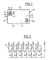
- Figure 1 shows a memory card according to the invention. It comprises a body 10 of plastic material (PVC or ABS for example) of generally rectangular parallelepipedal shape having two main faces: the face 12, visible in FIG. 1; and the side 14 not visible.
- the card body can also be made of polyester or paper.
- external electrical contact pads 16 to 30 which are connected to an electrical circuit mounted inside the card. These external areas are intended, when the card is inserted into a card reader, to allow the establishment of an electrical connection between the circuit of the card and the processing circuit of the card reader.
- the shape of the card body as well as the dimensions and positions of the external areas 16 to 30 are exactly identical to those of the corresponding elements of an electronic memory card.
- the card according to the invention is identical to a real electronic memory card.
- electronic memory cards must comply with either the ISO standard or the AFNOR standard. These standards define in particular the dimensions of the card body, the dimensions of the outer areas 16 to 30 and their position relative to the edges 32 and 34 of the card body. If the card according to the invention is intended for use in France, it therefore conforms to one of these two standards.
- the thickness of the card body is not a critical parameter for the use of a card in a reader conforming to the aforementioned standards. The thickness of the body of a card according to the invention may therefore, on this point, deviate from the standard. The only constraint from this point of view being that the card can be processed in a standard card reader.
- the storage circuit installed in the card body and connected to the external pads 16 to 30 is not produced in a semiconductor chip, but it is a question of 'an electrical circuit formed of discrete electrical elements, connected to the external pads by conductive elements.
- Each electrical element intended to constitute one or possibly several memory points is preferably connected to two external areas.
- the electrical element has an initial state of electrical conduction, this initial state being able to be modified by applying to the external areas associated with this electrical element a suitable electrical signal, analogous to a write signal.
- the electrical element is chosen in such a way that, when it has taken the modified state of conduction, it can no longer return to the initial state of conduction.
- each electrical element is constructed and mounted in such a way that, by applying to the areas associated with an electrical element a suitable electrical signal called a reading, it can be determined whether the electrical element is in its initial state or in a modified conduction state.
- each electrical element is associated with a pair of external pads.
- By applying an electrical write signal to the pair of tracks it is possible to modify the conduction state of the electrical element.
- By applying an electrical read signal to the pair of tracks it is possible to know whether the electrical element is in the initial state or in the modified state.
- card reader a card processing device usable with cards according to the invention.
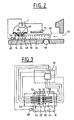
- Figures 2 and 3 show the general organization of such a reader which is identical to that of an electronic memory card reader. It comprises a slot 40 for inserting the card 10 which is extended by a guide passage 42 for the card.
- the corridor 42 is limited by a floor 44 and by side walls not shown.
- Inside the corridor 42 is mounted a connector 46.
- the connector 46 essentially comprises an insulating support 48 on which flexible conductive blades 50 to 64 are fixed. The number of blades is equal to the number of external areas of the card c ' ie eight in the example described.
- the card is brought into the treatment position either manually or by a drive system represented in FIG. 2 by a roller 66.
- each external pad 16 to 30 of the card 10 is in contact electric with one of the conductive blades.
- corridor 42 there is also mounted a card presence detector 68 which delivers a signal when the card has arrived in the processing position.
- the eight flexible blades 50 to 64 and the detector 68 are connected to a processing circuit 70 by electrical connections.
- the processing circuit 70 comprises parts already existing in the readers of electronic memory cards and specific parts which will be described in connection with FIG. 4.
- the reader must be able to process standard cards and cards according to the invention, the latter are provided on the face 12 of their body with a magnetic or optical mark.
- the reader is provided with a suitable detector 71 which triggers the specific process when a card according to the invention is inserted into the reader.
- connection circuit 72 is double. It allows on the one hand to connect supply terminals 74 and 76 to any two of conductors 1 to 8 and on the other hand to connect any two of conductors 1 to 8 to two terminals 78 and 80 for measurement.
- the supply terminals 74 and 76 are connected to a controllable voltage source 82 and the terminals 78 and 80 are connected to a voltage measurement circuit 84.
- a control circuit 86 has a first output 88 which is connected to the control input 90 of the connection circuit 72, and a second output 92 which is connected to the control input 94 of the voltage source 82.
- the circuit 86 also includes an input 96 on which it receives the result of the measurement carried out by circuit 84.
- the circuit 82 can deliver a first reading voltage V L which is insufficient to cause the change of conduction state of an electrical element of the card, and at least a second writing voltage V E which makes it possible to modify the conduction state of an electrical element of the card.
- the reader operates as follows: when a card 10 is inserted in the reader and it arrives in the processing position, the detector 68 sends to the sorting circuit 70 and more precisely to the control circuit 86 a signal which triggers the following operations.
- the circuit 82 is controlled to apply the reading voltage V L to the terminals 74 and 76, and the connection circuit 72 is controlled to connect simultaneously to the terminals 74, 76 and 78, 80 pairs of lines 1 to 8 in an order preset says write order in the card.
- the measuring device 84 delivers to the control circuit 86 a signal which indicates that the electrical element of the card is in the modified state. or in the initial state.
- connection circuit 72 As soon as the signal delivered by the measurement circuit indicates that the electrical element is in the initial state, the connection circuit 72 is maintained in the position it then occupies and upon receipt of a received registration signal on its input 98, the control circuit 86 can control the "toasting" of an electrical element, for example to authorize the obtaining of a telephone charging unit. On reception of the write signal, the control circuit 86 controls by its output 92 the voltage source 82 so that it delivers the write voltage V E. This causes the transition from the initial state to the modified state of the electrical element selected by connection circuit 72.
- control circuit 86 controls the voltage generator 82 so that it delivers the reading voltage V L in order to verify that the electrical element has indeed seen its conduction state be modified. Then the circuit 82 is controlled so as not to deliver any voltage and the connection circuit is controlled to connect to the next pair of lines. It is ready to "grill" a new electrical element on the card.
- FIG. 5 shows a first embodiment of the electrical circuit of the card and therefore of the electrical elements and of the connection elements.
- the external areas of electrical connection which in fact occupy on the body of the card the positions of the external areas 16 to 30 of Figure 1.
- Each electrical element is constituted by a fuse F i which is calibrated to remain intact (initial state when the read voltage V L is applied to it and to melt when the write voltage V E is applied to it.
- Each of the fuses F1 to F7 is mounted between range 1 and one of the ranges 2 to 8.
- the electrical circuit preferably comprises a second series of fuses F′1 to F′7, each of these fuses being mounted between one of ranges 2 to 7 and range 1 via a resistor R2 to R7 connected in series with the fuse F′1 to F′7.
- the resistors R1 to R7 are defined in such a way that, when write voltage V is applied E the current flowing through a fuse Fi is sufficient to melt it but that the current flowing through the corresponding fuse F ′ i is insufficient to produce the same effect.
- the "burnout" of the fuses F ′ i is obtained by applying to the pads corresponding a second write voltage V ′ E which is sufficient for the current flowing through the fuse F ′ i and the resistor R i to cause the latter to melt.
- V ′ E the voltage source 82 of the card reader
- the writing order consists in "blowing" first the fuses F i then, then, the fuses F ′ i . It is also necessary to provide two read voltages V L for fuses F i and V ′ L for fuses F ′ i .
- the voltage V′L can be identical to the voltage V E.
- a third series of fuses F ⁇ i could be provided, each mounted between one of terminals 2 to 7 and a resistor R ′ i connected to terminal 1, the fuse F ⁇ i and the corresponding resistor R ′ I being connected in series.
- the resistances R ′ i are all equal.
- the writing is done with a voltage V ⁇ E and the reading with a voltage V ⁇ L.
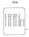
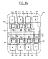
- FIGS 6a and 6b show a preferred embodiment of the electrical module according to the invention.
- an insulating support made of plastic material 100.
- metallizations 102 to 106 to form fuses F1 to F7 and F′1 to F′7.
- fuses they are preferably made in the following manner.
- a support sheet on which is fixed a conductive sheet, for example aluminum, of reduced thickness, for example 500A.
- the assembly is placed on the support 100 in such a way that the conductive sheet is in contact with the support 100.
- a tool which reproduces the shape of the metallizations 102 to 116 a sheet is applied to this sheet. pressure and a suitable temperature.
- An electrical module of very small thickness is thus obtained which can be inserted into the body 10 of the card by techniques already well known. It goes without saying that a plurality of electrical modules are produced on the same support sheet. Then cut this sheet to obtain the electrical modules.
- a second electrical module bearing the reference 200 can be produced using the same techniques as previously.
- the module 200 occupies, with respect to the edges 32 ′ and 34 ′, the same position as the first electrical module with respect to edges 32 and 34. This makes it possible to double the total number of memory points.
- the card holder inserts his card, edge 34 forward, into the card reader until he has used up the memory points of the first module electric, then he introduces his card, the edge 34 ′ forward until the second electric module is exhausted.
Landscapes
- Engineering & Computer Science (AREA)
- Physics & Mathematics (AREA)
- General Physics & Mathematics (AREA)
- Theoretical Computer Science (AREA)
- Artificial Intelligence (AREA)
- Computer Vision & Pattern Recognition (AREA)
- Credit Cards Or The Like (AREA)
- Control Of Vending Devices And Auxiliary Devices For Vending Devices (AREA)
Applications Claiming Priority (2)
| Application Number | Priority Date | Filing Date | Title |
|---|---|---|---|
| FR8808640A FR2633420B1 (fr) | 1988-06-28 | 1988-06-28 | Support d'informations et systeme de gestion de tels supports |
| FR8808640 | 1988-06-28 |
Publications (1)
| Publication Number | Publication Date |
|---|---|
| EP0349412A1 true EP0349412A1 (de) | 1990-01-03 |
Family
ID=9367782
Family Applications (1)
| Application Number | Title | Priority Date | Filing Date |
|---|---|---|---|
| EP89401821A Withdrawn EP0349412A1 (de) | 1988-06-28 | 1989-06-27 | Datenträger und Steuerungssystem dieser Träger |
Country Status (4)
| Country | Link |
|---|---|
| US (1) | US5086216A (de) |
| EP (1) | EP0349412A1 (de) |
| JP (1) | JPH0296889A (de) |
| FR (1) | FR2633420B1 (de) |
Cited By (6)
| Publication number | Priority date | Publication date | Assignee | Title |
|---|---|---|---|---|
| FR2695751A1 (fr) * | 1992-09-11 | 1994-03-18 | Laumonier Alain | Support d'informations à mémoire modifiable, lecteur de support d'informations adapté à utiliser un tel support, et système constitué par une tel lecteur. |
| WO1994015318A1 (de) * | 1992-12-23 | 1994-07-07 | GAO Gesellschaft für Automation und Organisation mbH | System zur echtheitsprüfung eines datenträgers |
| WO1995000925A1 (en) * | 1993-06-25 | 1995-01-05 | Cotag International Limited | Coding devices |
| WO1996023277A1 (en) * | 1995-01-27 | 1996-08-01 | Interprint Formularios Ltda. | Memory card and method of producing same |
| FR2745932A1 (fr) * | 1996-03-11 | 1997-09-12 | Gemplus Card Int | Ticket a contacts et lecteur associe |
| DE10018356A1 (de) * | 2000-04-13 | 2002-02-14 | Siemens Ag | Verfahren zum Identifizieren eines elektronischen Steuergeräts und dafür geeignetes Steuergerät |
Families Citing this family (14)
| Publication number | Priority date | Publication date | Assignee | Title |
|---|---|---|---|---|
| CA2073449C (en) * | 1990-01-15 | 1997-03-18 | Hans Olof Sjoblom | Handling system for information carriers |
| US5539402A (en) * | 1992-08-03 | 1996-07-23 | The United States Of America As Represented By The Administrator Of The National Aeronautics And Space Administration | System for memorizing maximum values |
| GB2327791B (en) * | 1997-07-25 | 2001-03-21 | Nokia Mobile Phones Ltd | A data card connector |
| US6601940B2 (en) | 1997-11-14 | 2003-08-05 | Canon Kabushiki Kaisha | Head, recording apparatus having the head, method for identifying the head, and method for giving identification information to the head |
| US6205030B1 (en) | 1999-05-26 | 2001-03-20 | 3Com Corporation | External fuse access for PC card |
| US6283773B1 (en) * | 1999-05-27 | 2001-09-04 | 3Com Corporation | Media jack with external fuse access |
| FR2808608A1 (fr) * | 2000-05-03 | 2001-11-09 | Schlumberger Systems & Service | Carte a memoire electronique destinee a etre introduite dans un dispositif de traitement |
| US7076663B2 (en) | 2001-11-06 | 2006-07-11 | International Business Machines Corporation | Integrated system security method |
| DE10338032B4 (de) * | 2003-08-19 | 2009-12-17 | Infineon Technologies Ag | Prozessor mit elektronischen Sicherungen zum Speichern von Geheimdaten |
| NO20052904L (no) * | 2005-06-14 | 2006-12-15 | Thin Film Electronics Asa | Et ikke-flyktig elektrisk minnesystem |
| US8649820B2 (en) | 2011-11-07 | 2014-02-11 | Blackberry Limited | Universal integrated circuit card apparatus and related methods |
| US8936199B2 (en) | 2012-04-13 | 2015-01-20 | Blackberry Limited | UICC apparatus and related methods |
| USD703208S1 (en) | 2012-04-13 | 2014-04-22 | Blackberry Limited | UICC apparatus |
| USD701864S1 (en) * | 2012-04-23 | 2014-04-01 | Blackberry Limited | UICC apparatus |
Citations (4)
| Publication number | Priority date | Publication date | Assignee | Title |
|---|---|---|---|---|
| FR2374702A1 (fr) * | 1976-12-14 | 1978-07-13 | Selenia Ind Elettroniche | Carte pour l'activation et pour la perception du paiement, constituee par un circuit electronique d'elements effacables, pour la distribution de denrees et de prestations, et machine fonctionnant avec cette carte |
| EP0144533A2 (de) * | 1983-12-03 | 1985-06-19 | Blaupunkt-Werke GmbH | Kreditkarte |
| EP0156980A1 (de) * | 1984-03-15 | 1985-10-09 | Siemens Aktiengesellschaft | Anordnung zur Kennzeichnung von elektronischen Schlüssel-/Schlosssystemen |
| FR2577334A1 (fr) * | 1985-02-08 | 1986-08-14 | Kalfon Rene | Carte a memoire electronique et lecteur de carte |
Family Cites Families (14)
| Publication number | Priority date | Publication date | Assignee | Title |
|---|---|---|---|---|
| FR577334A (fr) | 1923-04-07 | 1924-09-03 | Prec Electr | Perfectionnement aux appareils utilisant les lampes-relais dites triodes |
| US3702464A (en) * | 1971-05-04 | 1972-11-07 | Ibm | Information card |
| BE794202A (fr) * | 1972-01-19 | 1973-05-16 | Intel Corp | Liaison fusible pour circuit integre sur substrat semi-conducteur pour memoires |
| US3863261A (en) * | 1973-05-11 | 1975-01-28 | Electroprint Inc | Electrically addressed apertured modulator for electrostatic printing |
| US3872450A (en) * | 1973-06-21 | 1975-03-18 | Motorola Inc | Fusible link memory cell for a programmable read only memory |
| US3877049A (en) * | 1973-11-28 | 1975-04-08 | William D Buckley | Electrodes for amorphous semiconductor switch devices and method of making the same |
| DE2505186C3 (de) * | 1974-02-15 | 1979-07-12 | N.V. Philips' Gloeilampenfabrieken, Eindhoven (Niederlande) | Programmierbarer Lesespeicher |
| FR2311360A1 (fr) * | 1975-05-13 | 1976-12-10 | Innovation Ste Int | Systeme pour memoriser des donnees de maniere confidentielle au moyen d'objets portatifs electroniques comportant un circuit de memorisation des erreurs de code confidentiel |
| FR2334170A1 (fr) * | 1975-12-05 | 1977-07-01 | Honeywell Bull Soc Ind | Memoire morte integree |
| FR2501396B1 (fr) * | 1981-03-05 | 1985-10-11 | Dassault Electronique | Systeme de controle d'acces, notamment pour le passage de points de peage |
| JPS61264485A (ja) * | 1985-05-18 | 1986-11-22 | Hitachi Maxell Ltd | Icカ−ドのリ−ダ−・ライタ− |
| JPH0734313B2 (ja) * | 1985-08-09 | 1995-04-12 | 株式会社日立製作所 | Icメモリ装置 |
| JPS62291799A (ja) * | 1986-06-11 | 1987-12-18 | Fujitsu Ltd | 半導体記憶装置 |
| GB2206431B (en) * | 1987-06-30 | 1991-05-29 | Motorola Inc | Data card circuits |
-
1988
- 1988-06-28 FR FR8808640A patent/FR2633420B1/fr not_active Expired - Lifetime
-
1989
- 1989-06-27 EP EP89401821A patent/EP0349412A1/de not_active Withdrawn
- 1989-06-27 US US07/371,768 patent/US5086216A/en not_active Expired - Fee Related
- 1989-06-28 JP JP1166497A patent/JPH0296889A/ja active Pending
Patent Citations (4)
| Publication number | Priority date | Publication date | Assignee | Title |
|---|---|---|---|---|
| FR2374702A1 (fr) * | 1976-12-14 | 1978-07-13 | Selenia Ind Elettroniche | Carte pour l'activation et pour la perception du paiement, constituee par un circuit electronique d'elements effacables, pour la distribution de denrees et de prestations, et machine fonctionnant avec cette carte |
| EP0144533A2 (de) * | 1983-12-03 | 1985-06-19 | Blaupunkt-Werke GmbH | Kreditkarte |
| EP0156980A1 (de) * | 1984-03-15 | 1985-10-09 | Siemens Aktiengesellschaft | Anordnung zur Kennzeichnung von elektronischen Schlüssel-/Schlosssystemen |
| FR2577334A1 (fr) * | 1985-02-08 | 1986-08-14 | Kalfon Rene | Carte a memoire electronique et lecteur de carte |
Cited By (8)
| Publication number | Priority date | Publication date | Assignee | Title |
|---|---|---|---|---|
| FR2695751A1 (fr) * | 1992-09-11 | 1994-03-18 | Laumonier Alain | Support d'informations à mémoire modifiable, lecteur de support d'informations adapté à utiliser un tel support, et système constitué par une tel lecteur. |
| WO1994015318A1 (de) * | 1992-12-23 | 1994-07-07 | GAO Gesellschaft für Automation und Organisation mbH | System zur echtheitsprüfung eines datenträgers |
| WO1995000925A1 (en) * | 1993-06-25 | 1995-01-05 | Cotag International Limited | Coding devices |
| WO1996023277A1 (en) * | 1995-01-27 | 1996-08-01 | Interprint Formularios Ltda. | Memory card and method of producing same |
| US5837367A (en) * | 1995-01-27 | 1998-11-17 | Interprint Formularios Ltda. | Memory card and method of producing same |
| FR2745932A1 (fr) * | 1996-03-11 | 1997-09-12 | Gemplus Card Int | Ticket a contacts et lecteur associe |
| DE10018356A1 (de) * | 2000-04-13 | 2002-02-14 | Siemens Ag | Verfahren zum Identifizieren eines elektronischen Steuergeräts und dafür geeignetes Steuergerät |
| DE10018356B4 (de) * | 2000-04-13 | 2005-05-04 | Siemens Ag | Verfahren zum Identifizieren eines elektronischen Steuergeräts und dafür geeignetes Steuergerät |
Also Published As
| Publication number | Publication date |
|---|---|
| FR2633420A1 (fr) | 1989-12-29 |
| US5086216A (en) | 1992-02-04 |
| JPH0296889A (ja) | 1990-04-09 |
| FR2633420B1 (fr) | 1992-02-21 |
Similar Documents
| Publication | Publication Date | Title |
|---|---|---|
| FR2633420A1 (fr) | Support d'informations et systeme de gestion de tels supports | |
| EP0376062B1 (de) | Elektronisches Modul mit einer integrierten Schaltung für ein kleines tragbares Objekt, z.B. eine Karte oder ein Schlüssel und Herstellungsverfahren für solche Module | |
| EP1692642B1 (de) | Sicherheitsdokument mit einem kontaktlosen chip mit datenmaskierung | |
| EP0241379B1 (de) | Vorrichtung zur Behandlung von elektronischen Speicherkarten zum Liefern von Leistungen | |
| FR2743649A1 (fr) | Module electronique sans contact, carte etiquette electronique l'incorporant, et leurs procedes de fabrication | |
| CH619310A5 (en) | Portable card for signal processing system and method of manufacturing this card | |
| EP2194489A1 (de) | Elektronische Karte, die Steuermittel umfasst | |
| EP0307773A1 (de) | Verfahren zur Herstellung elektronischer Module, insbesondere für Informationskarten | |
| EP1116179B1 (de) | Kontaktlose chipkarte mit hemmungsmitteln | |
| EP3734493A1 (de) | Aufnahmeetui für chipkarte | |
| WO1996029671A1 (fr) | Cadre de lecture pour appareil lecteur de carte a microcircuit | |
| FR2852886A1 (fr) | Cartouche d'impression securisee | |
| WO2011012797A2 (fr) | Telephonie mobile et communication nfc | |
| FR2893161A1 (fr) | Document a microcircuit electronique sans contact et capteur de proximite. | |
| EP0815529B1 (de) | Verbinder für ic-kartenleser | |
| EP4002194B1 (de) | Vorrichtung zur erfassung einer mikroschaltkreiskarte | |
| EP1476849B1 (de) | Elektromagnetischer transponder mit programmierbarem code | |
| FR2610754A1 (fr) | Transducteur d'echange de donnees pour carte a circuit integre | |
| EP1055195B1 (de) | Verfahren zur herstellung einer ic-karte | |
| FR2727225A1 (fr) | Objet portatif comprenant un circuit electronique alimente par pile interne et comportant une memoire de donnees, procede et dispositif d'alimentation externe de cet objet et de transfert de donnees avec celui-ci | |
| FR2638265A1 (fr) | Support d'informations et systeme de gestion de tels supports | |
| FR2745932A1 (fr) | Ticket a contacts et lecteur associe | |
| FR2659767A1 (fr) | Circuit de caracterisation de microcircuits, lecteur enregistreur de carte a microcircuits, et carte a microcircuits associee. | |
| FR2695751A1 (fr) | Support d'informations à mémoire modifiable, lecteur de support d'informations adapté à utiliser un tel support, et système constitué par une tel lecteur. | |
| EP0266229A1 (de) | Tastatur mit Lesevorrichtung |
Legal Events
| Date | Code | Title | Description |
|---|---|---|---|
| PUAI | Public reference made under article 153(3) epc to a published international application that has entered the european phase |
Free format text: ORIGINAL CODE: 0009012 |
|
| AK | Designated contracting states |
Kind code of ref document: A1 Designated state(s): BE CH DE ES GB GR IT LI NL SE |
|
| 17P | Request for examination filed |
Effective date: 19900213 |
|
| 17Q | First examination report despatched |
Effective date: 19921124 |
|
| STAA | Information on the status of an ep patent application or granted ep patent |
Free format text: STATUS: THE APPLICATION IS DEEMED TO BE WITHDRAWN |
|
| 18D | Application deemed to be withdrawn |
Effective date: 19930406 |