EP1476849B1 - Elektromagnetischer transponder mit programmierbarem code - Google Patents
Elektromagnetischer transponder mit programmierbarem code Download PDFInfo
- Publication number
- EP1476849B1 EP1476849B1 EP03718862A EP03718862A EP1476849B1 EP 1476849 B1 EP1476849 B1 EP 1476849B1 EP 03718862 A EP03718862 A EP 03718862A EP 03718862 A EP03718862 A EP 03718862A EP 1476849 B1 EP1476849 B1 EP 1476849B1
- Authority
- EP
- European Patent Office
- Prior art keywords
- transponder
- resistor
- current
- code
- programming
- Prior art date
- Legal status (The legal status is an assumption and is not a legal conclusion. Google has not performed a legal analysis and makes no representation as to the accuracy of the status listed.)
- Expired - Lifetime
Links
Images

Classifications
-
- G—PHYSICS
- G06—COMPUTING; CALCULATING OR COUNTING
- G06K—GRAPHICAL DATA READING; PRESENTATION OF DATA; RECORD CARRIERS; HANDLING RECORD CARRIERS
- G06K19/00—Record carriers for use with machines and with at least a part designed to carry digital markings
- G06K19/06—Record carriers for use with machines and with at least a part designed to carry digital markings characterised by the kind of the digital marking, e.g. shape, nature, code
- G06K19/067—Record carriers with conductive marks, printed circuits or semiconductor circuit elements, e.g. credit or identity cards also with resonating or responding marks without active components
- G06K19/07—Record carriers with conductive marks, printed circuits or semiconductor circuit elements, e.g. credit or identity cards also with resonating or responding marks without active components with integrated circuit chips
-
- G—PHYSICS
- G11—INFORMATION STORAGE
- G11C—STATIC STORES
- G11C17/00—Read-only memories programmable only once; Semi-permanent stores, e.g. manually-replaceable information cards
- G11C17/14—Read-only memories programmable only once; Semi-permanent stores, e.g. manually-replaceable information cards in which contents are determined by selectively establishing, breaking or modifying connecting links by permanently altering the state of coupling elements, e.g. PROM
-
- G—PHYSICS
- G06—COMPUTING; CALCULATING OR COUNTING
- G06K—GRAPHICAL DATA READING; PRESENTATION OF DATA; RECORD CARRIERS; HANDLING RECORD CARRIERS
- G06K19/00—Record carriers for use with machines and with at least a part designed to carry digital markings
- G06K19/06—Record carriers for use with machines and with at least a part designed to carry digital markings characterised by the kind of the digital marking, e.g. shape, nature, code
- G06K19/067—Record carriers with conductive marks, printed circuits or semiconductor circuit elements, e.g. credit or identity cards also with resonating or responding marks without active components
- G06K19/07—Record carriers with conductive marks, printed circuits or semiconductor circuit elements, e.g. credit or identity cards also with resonating or responding marks without active components with integrated circuit chips
- G06K19/0723—Record carriers with conductive marks, printed circuits or semiconductor circuit elements, e.g. credit or identity cards also with resonating or responding marks without active components with integrated circuit chips the record carrier comprising an arrangement for non-contact communication, e.g. wireless communication circuits on transponder cards, non-contact smart cards or RFIDs
Definitions
- the present invention relates to an electromagnetic transponder, that is to say a transceiver (usually mobile) able to be interrogated, contactless and wireless, by a unit (usually fixed), called read terminal and / or writing.
- the transponders extract the power required for the electronic circuits they comprise from a high frequency field radiated by an antenna of the reading and writing terminal.
- read-only transponders that is, capable of operating with a terminal merely reading transponder data
- read-write transponders which contain data that can be modified by the terminal.
- Systems using electromagnetic transponders are based on the use of oscillating circuits comprising an antenna winding, transponder side and read / write terminal side. These circuits are intended to be coupled by close magnetic field when the transponder enters the field of the read / write terminal.
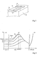
- the figure 1 represents, very schematically and simplified, a conventional example of a data exchange system between a read-write terminal 1 and a transponder 10 of the type to which the present invention applies.
- the terminal 1 consists essentially of a series oscillating circuit, formed of an inductor L1, in series with a capacitor C1 and a resistor Rb, between an output terminal 2 of an amplifier or antenna coupler (no shown) and a reference terminal 3 (usually ground).
- the antenna coupler is part of a circuit 4 for controlling the oscillating circuit and for operating the received data including, inter alia, a modulator / demodulator and a microprocessor for the processing of commands and data.
- the circuit 4 of the terminal generally communicates with different input-output circuits (keyboard, screen, means of exchange with a server, etc.) and / or processing not shown.
- the circuits of the read / write terminal draw the energy necessary for their operation from a supply circuit (not shown) connected, for example, to the electrical distribution network.
- a transponder 10 intended to cooperate with a terminal 1, essentially comprises a parallel oscillating circuit formed by an inductance L2, in parallel with a capacitor C2, between two input terminals 11, 12 of a control circuit 13 and treatment.
- Terminals 11 and 12 are, in practice, connected to the input of a rectifying means (not shown in FIG. figure 1 ) whose outputs constitute terminals for continuous supply of internal circuits to the transponder.
- These circuits generally comprise, essentially, a microprocessor or a wired logic circuit, a memory, a demodulator of the signals possibly received from the terminal 1, and a modulator for transmitting information to the terminal.
- this information is most often constituted by a (binary) code enabling the processing system, on the terminal 1 side, to identify the product. with which the label is associated.
- the oscillating circuit of the terminal 1 is excited by a high frequency signal (for example, 13.56 MHz) intended to be 10 when the transponder 10 is in the field of the terminal 1, a high frequency voltage is generated at the terminals 11, 12 of the resonant circuit of the transponder.
- This voltage after rectification and possible clipping, is intended to provide the supply voltage of the electronic circuits 13 of the transponder.
- the oscillating circuits of the terminal and the transponder are generally tuned to the same frequency corresponding to the frequency of the excitation signal of the oscillating circuit of the terminal 1.
- This high frequency signal (for example, 13.56 MHz) serves as the carrier of remote power supply for transponders in the field of the terminal and, where appropriate carrier of data transmission from the terminal to this or these transponders.
- a transponder When a transponder is in the field of a terminal 1, a high frequency voltage is generated at terminals 11 and 12 of the resonant circuit of the transponder. This voltage, after rectification and possible clipping, provides the supply voltage of the electronic circuits 13 of the transponder.
- the high frequency carrier transmitted by the terminal is generally amplitude modulated by the latter according to different coding techniques in order to transmit data and / or commands to one or more transponders in the field.
- the transmission of data from the transponder to the terminal is generally effected by modulating the load formed by the resonant circuit L2, C2.
- This load variation (called retromodulation) is carried out at the rate of a subcarrier frequency (for example, 847.5 kHz) lower than that of the carrier.
- This charge variation can then be detected by the terminal in the form of a variation of amplitude or of a phase variation by means of, for example, a measurement of the voltage across the capacitor C1 or the current in the oscillating circuit.
- the measuring signal has been symbolized by a dotted line connecting the midpoint between the inductor L1 and the capacitor C1 to the circuit 2.
- the retromodulation carried out by the transponder can be resistive or capacitive.
- the invention relates to a resistive retromodulation transponder.
- the resistive retromodulation consists in connecting, in parallel on the resonant circuit L2, C2, a resistor in series with a switch (generally a MOS transistor).
- the switch is controlled according to the code to be transmitted (0 or 1) to the rhythm of the sub-carrier.
- the parallel connection is generally performed downstream of the rectifier bridge.
- transponder More and more, it is sought to integrate the entire transponder into the same silicon chip (L2 antenna, capacitor C2 and circuit 13). In addition, it seeks to minimize the surface of this chip to miniaturize the transponders, particularly in applications to electronic tags. An electronic tag can then replace the printing of a conventional bar code to contain the identifier of a product.
- a problem of conventional transponders is related to the need to use a modulator-demodulator to convert a code (digital data, identification code of a label, etc.) to be transmitted to the read-write terminal.
- This requirement entails the necessary recourse to a storage memory (for example, a RAM, ROM, EPROM, or EEPROM) of the code in binary form and to a modulation circuit upstream of the resistive retromodulation elements themselves.
- This complexity is detrimental to the miniaturization and cost of current transponders.
- Another disadvantage is that the programming of a binary code and, more generally, the writing of data in an electromagnetic transponder, requires at best a communication with a read-write terminal and a complex exchange protocol. At worst, in the case where one wishes to store immutable code in a single programming memory, it is necessary to enter this code during manufacture in an EPROM or an EEPROM.
- Another known technique is to increase the value of a resistor by subjecting it optically to a laser physically reducing its size.
- a disadvantage is the exorbitant cost of the operation that must be repeated for each chip.
- Another disadvantage is that the manipulation is visible optically, therefore detectable.
- the document GB-A-2,279,474 discloses a coding device for a radio frequency tag having a parallel oscillating circuit for extracting a radiated field from a supply signal.
- WO 97/05665 discloses a memory element consisting of a resistor that can take a plurality of resistance values using a programming current.
- the present invention aims to overcome the disadvantages of conventional transponders.
- the invention aims to provide an electromagnetic transponder avoiding the use of a digital modulator for transmitting data stored in storage elements.
- the invention also aims to preserve the compatibility of the transponder with the existing read-write terminals.
- the invention also aims to allow a simple programming of a binary code in an electromagnetic transponder: In particular, the invention aims to avoid the use of bidirectional communication to enter a code in a transponder.
- the invention aims to enable the transmission, by an electromagnetic transponder, of any message without the need to resort to a data modulator stored in a digital memory.
- the invention also aims to make undetectable, out of operation, a code stored in an electromagnetic transponder.
- the invention also aims to allow programming after manufacturing of the integrated circuit, while it is in its application environment.
- the resistors are of polycrystalline silicon and are dimensioned to have identical nominal values.
- the programming of a code portion in a resistor is controlled by forcing the flow of a current in the polycrystalline silicon resistance which is greater than the current for which the value of this resistance is maximum.
- the programming current is extracted from a field radiated by a read-write terminal, with a power greater than the power of a read-beam field.
- the cyclic control element consists of a shift register controlled by a clock signal, each switch being controlled by a bit of the shift register.
- the clock signal is extracted from the field radiated by a read-write terminal.
- an initialization input of the shift register is connected to the output of a NOR-type logic gate whose inputs receive, in parallel, the bits of the shift register.
- the transponder comprises a stored code lock circuit prohibiting a second programming.
- the locking circuit comprises a limiting element of the voltage at the terminals of said branches, the regulation setpoint being a function of an additional storage resistor polycrystalline silicon whose value is decreased at the end of programming.
- the transponder comprises a set of synchronizing branches each consisting of a stall resistance and a control switch, said synchronizing branches being controlled by said cyclic control element.
- the programmable resistors are programmed to values chosen from among several values, so as to store a multilevel code.
- all its constituents are integrated on the same chip, devoid of input-output pad.
- the invention also provides a method of programming a code in a transponder, consisting in imposing temporarily and successively, in each of the resistors whose state is desired to change with respect to the non-programmed state, the circulation of a current stress greater than a current for which the value of this resistance has a maximum.
- the stress current is chosen from a predetermined table of correspondence between the stress current and the desired final resistance.
- the constraint current is chosen from among several values for storing a multilevel code.
- a feature of the present invention is to use, as a storage element of data to be transmitted, directly the resistance value of a retromodulation element consisting of a switch in series with a resistor.
- a retromodulation element consisting of a switch in series with a resistor.
- the resistances of the different elements have different values depending on the state (for example, 0 or 1) of the part of code they transmit.
- the invention makes use of the fact that, by charging the transponder oscillating circuit differently, this difference can be interpreted by the terminal as meaning a different state of the bit transmitted by the transponder in its field.
- the resistors of the different branches of retromodulation in parallel are all manufactured identically in polycrystalline silicon and have the same nominal value.
- the programming is then performed by causing a decrease, stable and irreversible, the value of the resistance associated with the branch as it will be better understood in relation to the Figures 3 and 4 .
- the figure 2 represents an embodiment of an electromagnetic transponder 20 according to the present invention.
- the transponder 20 comprises a parallel oscillating circuit formed of an inductance L2, in parallel with a capacitor C2, between two terminals 11, 12 of an input of a control and processing circuit 23.
- the terminals 11 and 12 are connected to the input of a rectifying bridge 24 or equivalent, the outputs of which constitute terminals 25, 26 for the continuous supply of the circuits internal to the transponder.
- the circuit 23 comprises, in parallel between the terminals 25 and 26 of the output of the bridge 24, several (n) resistive retromodulation elements each consisting of a resistor Rpi (i being between 1 and n) and d a control switch Mi (for example, a MOS transistor).
- Each retromodulation element is, according to the invention, an element for storing part of the code. In fact, the value of the resistance Rpi of each element is used to distinguish one state from another for the part of the code represented by the element concerned.
- the retromodulation elements are connected between the terminals 11 and 12.
- each element is associated with at least one rectifying diode and the retromodulation preferably operates only on half of the signal of high frequency excitation (for example, the 13.56 MHz remote power carrier).
- bridge 24 has the advantage of saving space (fewer diodes).
- each element representing a bit of the code.
- the invention more generally applies to multi-level or even analog coding, insofar as the slightest difference in value between two resistors of two retromodulation elements generates a difference in the load represented by the transponder on the circuit. oscillating from an excitation and reading terminal.
- the control of the transistors Mi is carried out in all or nothing. According to the invention, this command is carried out successively for each branch.
- a cyclic control is provided so that the code represented by the sequence of bits (in the binary case) is transmitted repeatedly, as long as the transponder is in the field of a reading terminal.
- a shift register 27 on n bits Bi (as much as retromodulation elements to be controlled) or n + 1 bits is used for this purpose if a latch circuit 40 of the programmed code is provided.
- the output bits of the shift register are taken in parallel in the direction of the control gates of the transistors Mi.
- each bit of the shift register is supplied to a transistor Mi.
- the register is at "1" circulating, that is to say that one bit of the register is in the high state (1), the other bits being in the low state (0) to block the n -1 remaining Mi transistors.
- the obtaining of the "1" circulating at the input of the register comes, for example, from a logic gate 28 of NOR type (NOR) receiving as inputs the n bits of the shift register taken in parallel and whose output provides the bit B1 status at startup (initialization).
- NOR NOR type
- the gate 28 allows an automatic start of the register as soon as it is powered.
- the register shift sequencing is provided by a CLK clock signal deriving the clock frequency from the high frequency excitation signal from the terminal.
- a frequency divider 29 is connected between the terminals 25 and 26 (alternatively between the terminals 11 and 12), and its output is connected to the clock input of the shift register 27. division of the divider 29 depends on the frequency of the back-modulation subcarrier of the system. With the example of a carrier at 13.56 MHz and a subcarrier at 847.5 kHz, the division rate is 16.
- the supply of the register 27, the gate 28 and the divider 29, comes from a voltage regulator 30 connected between the terminals 25 and 26 and the output of which provides a supply voltage ALIM continuous and regulated in a conventional manner.
- Circuit 23 of the figure 2 further comprises, according to a preferred embodiment, a circuit 40 for locking the programmed code.
- This circuit comprises, in the illustrated embodiment, an n + 1 th retromodulation element consisting of a resistor Rpn + 1 and a transistor Mn + 1.
- the midpoint of the series connection of the transistor and the resistor is connected to the gate of an N-channel MOS transistor T connected between terminals 25 and 26, and a resistor Rt to terminal 26 (constituting in this example, the mass).
- the gate of the transistor Mn + 1 is connected at the output of an n + 1 th bit of the shift register 27.
- the operation of the circuit 40 will be explained later, in connection with the preferred embodiment of programming. For the moment, it will be noted simply that this circuit 40 operates, after programming, as a regulator preventing the voltage between terminals 25 and 26 from exceeding a value likely to cause reprogramming.
- the code stored in a transponder is read as follows.
- the transponder At rest, all Mi transistors are blocked, the transponder is not powered (it does not have a standalone power supply). As soon as the transponder enters the field of a read / write terminal, it captures the remote power carrier. Indeed, a terminal of a transponder system without autonomous power continuously emits to "wake up" the transponders that enter his field. Thus, as soon as the transponder enters the field, a voltage appears between the terminals 25 and 26. The regulator 30 then produces a supply voltage of the various elements.
- the transponder issues his code. Indeed, since initially no bit of the register contains a high state, the gate 28 provides a high state at the input of the register 27. The clock signal causes the storage of this state 1 in the bit B1. This results in a closure of the switch M1, so a retromodulation with the resistor R1. Depending on the value of the resistor R1, the signal interpreted by the terminal provides a 1 or a 0. The transmission of the first bit is conditioned by the CLK signal (which corresponds to the retromodulation subcarrier).
- bit B1 is transferred to bit B2. This causes the transistor M1 to open and the transistor M2 to close, and so on.
- the content of bit B1 is replaced by the state present at the output of gate 28. However, as soon as a state 1 is present in the register, so as soon as the first bit B1 is loaded at start-up, this output switches to FIG. low state (0) and remains there until the extinction of the system by disappearance of the supply, thus until exit of the transponder out of the field of the terminal.
- All the transistors Mi are therefore successively controlled at the rhythm of the clock CLK, which causes the emission, by retromodulation of the carrier of remote power supply, code stored by the resistors Rpi.
- the transmission of the code is repeated cyclically as long as the transponder remains powered by its presence in the field of the terminal. Even if, temporarily, two retromodulation branches are active during the shifting of the "1" flowing in the register, the duration of this simultaneous conduction of two transistors Mi is negligible compared to the retromodulation period (for example, 847.5 kHz) and will not be not taken into account by the terminal as another part of the code.
- Such an operation is particularly suitable for electromagnetic labels or the like, for which it is desired that they contain a code (generally identifying the product which carries them), and that this code is detected by the passage of the product in the field of a terminal (detection gantry, cash register, etc.).
- a code generally identifying the product which carries them
- a transponder according to the invention comprises simple and small numbers of components. It is not necessary to use a digital memory imposing addressing and read / write circuits, nor a modulator / demodulator to provide the code.
- a transponder according to the invention can dispense with a microprocessor.
- the realization of polycrystalline silicon resistors requires no additional step compared to those required for the implementation of a MOS technology in which can be made all the components (with the exception of inductance L2).
- the inductor is usually integrated on the same chip. The transponder of the invention is therefore particularly interesting for constituting an electronic tag.
- the programming of a code in a transponder is carried out as follows.
- all the Rpi resistors are manufactured identically, so that they all have the same nominal value. This nominal value conditions an unscheduled state of the retromodulation element and corresponds, for a binary code, to one of the two states (0 or 1).
- a feature of the present invention is to provide a programming of a retromodulation element to a state other than the unprogrammed state by causing an irreversible decrease in the value of its resistance Rpi. For this, it imposes the flow of a current in this resistance which is greater than the current for which the value of the resistance has a maximum.
- This characteristic of the invention will be better understood later in connection with the Figures 3 and 4 . For the moment, it will suffice to say that, if a sufficient current is circulated in a resistor Rpi, an irreversible decrease in the value of this resistor occurs when a nominal current (corresponding to range of operating currents for which it is designed).
- the programming current (of the order of one to ten milliamps) is beyond the range of currents (up to one hundred microamperes) of operation.
- the terminals of the resistors Rpi are accessible, preferably via a multiplexer type selector, from terminals of the integrated circuit chip.
- the programming is performed by applying, at the terminals of each resistor whose value is to be reduced, a programming voltage permitting the circulation of the programming current.
- a programming voltage permitting the circulation of the programming current.
- individual accesses can be provided by pads at the terminals of each resistor.
- the resistor Rpn + 1 is, at the end of the programming of all the other resistances, programmed in reduction of its value.
- the transponder is programmed in radiofrequency mode.
- sufficient for the current flowing in one of the selected resistors Rpi causes the decrease in value of this resistance.
- the first power is still sufficient to power the transponder and allow the operation of its constituents.
- the modulation of the transmission power corresponds to the binary code to be stored in the transponder.
- the modulation is performed at the rate of the transponder retromodulation frequency. Thus, it is not necessary to control independently the passage of a retromodulation element to the next, this passage is performed automatically by the shift register 27 of the transponder.
- the programming must start with the resistance Rp1 to end with the resistance Rpn + 1. Indeed, initially, the resistors all have their nominal value, including the resistance Rpn + 1 which is also in polycrystalline silicon. This resistor Rpn + 1 is, in manufacturing, sized so that the transistor T limits the voltage between the terminals 25 and 26, at a so-called level of programming.
- the resistor Rt forms, with the resistor Rpn + 1, a control voltage divider of the limiting transistor T.
- the resistor Rt is cyclically short-circuited by the transistor Mn + 1, which causes the blocking of the transistor T.
- the transmit power of the terminal is at the programming level when the resistance Rpn + 1 is reached.
- the result is a decrease in the value of this resistance, which modifies the relationship between resistors Rpn + 1 and Rt.
- the resistors Rpn + 1 and Rt are dimensioned so that, once the value of the resistor Rpn + 1 is reduced, the transistor T limits the voltage between the terminals 25 and 26 to a level lower than programming level (transistor T preferably operates in linear mode). Therefore, the transponder is protected against reprogramming, even if it is then subjected to a field accidentally sufficient to, in principle, cause a change in value of the resistors.
- the voltage at which the transistor T limits the voltage corresponds to the operating voltage. It suffices that it does not allow to reach the programming voltage, that is to say, as will be seen later, a voltage such that the current imposed on the resistors is greater than a current for which these resistances present a maximum value.
- the presence of the circuit 40 causes that, in reading, the code has a predetermined bit at the end. This is not a problem, however.
- the shift circuit illustrated by the figure 2 is compatible with the respect of the constraints due to the last programming of the resistance Rpn + 1. Indeed, as the gate 28 controls the register so that it starts at bit B1 when the transponder is powered, it is sufficient that it triggers the start of the transmitter (the terminal) when the transponder is in the field , that is to say nearby. In practice, this is not a constraint because programming is a voluntary and special operation.
- first group of back modulation branches (first set of resistors) programmable at the end of manufacture to contain a "manufacturer" code.
- the rest of the branches are left available to be programmed (in one or more times) by the user (final or not).
- a controlled synchronization of the shift register with the terminal For example, it can be provided that the terminal will first emit at low power (read power) and that the transponder has a number of chop resistors dimensioned in manufacture to give, for example, the opposite state of the resistors Rpi no programmed.
- the chock resistors provide a predetermined code. By analyzing the retromodulation, the terminal is then able to detect the position of the first programmable resistor in the cyclic reading, in order to synchronize the start of its power modulation.
- the shim resistors are of course also associated with a control transistor and a bit of the shift register. It follows that they are also involved in reading.
- the figure 3 represents an embodiment of a polycrystalline silicon resistor used to form the resistors Rpi of the retromodulation elements according to the preferred embodiment of the invention.
- Such resistance consists of a track (also called bar) polycrystalline silicon obtained by etching a layer deposited on an insulating substrate 32.
- the substrate 32 is indifferently directly constituted by the substrate of the integrated circuit carrying the transponder or consists of an insulating layer forming an insulating substrate or equivalent for the resistor 31.
- the resistor 31 is connected, at its two ends, to conductive tracks (for example, metal) 33 and 34 for connecting the resistive bar to the other elements of the integrated circuit.
- the schematic representation of the figure 3 does not refer to the various insulating and conductive layers generally constituting the integrated circuit.
- the resistive bar 31 placed on the insulating substrate 32 and in contact, by the ends of its upper face, with the two metal tracks 33 and 34.
- the links of the element resistive 31 to the other components of the integrated circuit are obtained by wider polysilicon tracks starting from the ends of the bar 31 in alignment thereof.
- the resistive element 31 is generally formed by making a section of a polycrystalline silicon track narrower than the rest of the track.
- the resistivity p of the element 31 depends, among other things, on the possible doping of the polycrystalline silicon constituting it.
- R ⁇ resistance square
- the quotient L / 1 corresponds to what is called the number of squares (square number) constituting the resistive element 31. This represents, seen from above, the number of squares of given dimension depending on the technology, put side by side. coast to form the element 31.
- the value of the polycrystalline silicon resistance is therefore defined, in the manufacture, according to the above parameters, leading to so-called nominal resistivities and resistances.
- the thickness e of the polycrystalline silicon is fixed by other manufacturing parameters of the integrated circuit. For example, this thickness is set by the desired thickness for the gates of the MOS transistors of the integrated circuit.
- a feature of the present invention is to impose temporarily, in a polycrystalline silicon resistor (Rpi) which it is desired to irreversibly reduce the value for modifying the charge level generated on the transponder's oscillating circuit and thus encoding a different state, a programming or stress current higher than a current for which the resistance passes through a maximum value, this current being beyond the range of normal operating currents (in retromodulation) of this resistance.
- the resistivity of the polycrystalline silicon in the operating current range is reduced, stably and irreversibly, by temporarily imposing in the corresponding resistive element the flow of a current beyond the current range.
- Another feature of the invention is that the current used to reduce the value of the resistance is, unlike a fuse element, non-destructive for the polycrystalline silicon element.
- the figure 4 illustrates, by a network of curves giving the resistance of a polycrystalline silicon element of the type represented by figure 3 as a function of the current flowing through it, an embodiment of the present invention for stabilizing a cell by reducing the value of one of its resistances.
- the polycrystalline silicon used in the manufacture of the resistive element 31 has a nominal resistivity conferring on the element 31, for the dimensions 1, L and e data, a resistance value R nom .
- This nominal (original) value of the resistor corresponds to the value stably taken by the resistive element 31 in the operating current range of the system, that is to say generally for currents smaller than 100 ⁇ A. .
- a current (for example I1) of the resistive element 31 constraint greater than a current Im for which the value of the resistance R of the element 31 is maximum without being infinite.
- a stable resistance of value R1 is obtained in the range A1 of the operating currents of the integrated circuit.
- the pace S name of resistance versus current is stable for relatively low currents (less than 100 ⁇ A). This pace starts to grow for currents significantly higher of the order of a few milliamperes or more (A2 range).
- FIG 4 there is illustrated a third A3 range of currents corresponding to the range generally used to make fuses. These are currents of the order of a tenth of an ampere where the resistance begins to grow abruptly until it becomes infinite. Therefore, it can be considered that the invention uses the intermediate range A2 of currents between the operating range A1 and the destructive range A3, to irreversibly reduce the value of the resistance or more precisely the resistivity of the element. polycrystalline silicon.
- the value taken by the resistor in the range of operating currents is lower than the value R nom .
- the new value, for example R1 depends on the highest value of the current (here, I1) that was applied during the irreversible decrease phase. It will be noted that the irreversible reduction effected by the invention is carried out in a specific phase of personalization of the transponder by writing the code, outside the normal reading operation (range A1) of the integrated circuit, that is to say out of normal operation of the resistor.
- a resistance value corresponds in fact to a decrease in the resistivity of the polycrystalline silicon constituting the resistive element.
- the inventors consider that there is a stable modification of the crystalline structure of polycrystalline silicon and that we are seeing, as it were, a creep of the material, the final crystalline structure obtained depending on the maximum current reached.
- a polycrystalline silicon resistor according to the invention does not differ from the realization of a conventional resistor.
- a layer of polycrystalline silicon is deposited which is etched according to the desired dimensions for the resistance. Since the thickness of polycrystalline silicon deposited is generally fixed by the technology, the two dimensions that can be adjusted are the width and the length. Generally, an insulation is redeposited on the polycrystalline silicon rod thus obtained.
- the width 1 will have been modified with respect to the wider access tracks to be highly conductive.
- vias will be made in the overlying insulator (not shown) of the polycrystalline silicon bar to connect contact metal tracks 33 and 34.
- the minimum thickness and minimum width for the resistive elements will be sought.
- the length L conditions the nominal value of the resistor once the polycrystalline silicon structure is fixed.
- the possible doping of polycrystalline silicon, whatever its type, does not hinder the implementation of the invention.
- the only difference related to doping is the nominal resistivity before stress and the resistivities obtained for given stress currents. In other words, for an element of given dimensions, this conditions the starting point of the value of the resistance, and consequently the resistance values obtained for given stress currents.
- the various currents to be determined apply to pass different resistance values to lower values.
- a test resistor is used which is subjected to a stepwise increase in current, returning after each increase in the range of operating currents to measure the obtained resistance value.
- the measured values will follow the Snom curve. Therefore, the currents (I1, I2, figure 4 ) and the associated resistors (R1, R2).
- the difference between the values of the table thus obtained depends on the step chosen for the increase by step of the stress current. This predetermination of course takes into account the nature of the polycrystalline silicon used as well as preferably the resistance per square, that is to say the resistivity of the material and the thickness in which it is deposited.
- the gaits illustrated by the figure 4 can also be read as the resistance of the resistance by tile, it is possible to transpose the calculated values to different resistors of an integrated circuit defined by the widths and lengths of the resistive sections. It is then possible to predetermine the value of the stress current to be applied to the resistive element in order to irreversibly and stably reduce its value. This determination makes it possible to fix the electromagnetic field, and therefore the transmission power, which the programming terminal must provide in the preferred embodiment of non-contact programming, by high frequency. In the simplified embodiment where mechanical access (pads) is provided to impose a programming voltage between terminals 25 and 26, this makes it possible to set the necessary programming voltage.
- the accuracy of the stress current is not critical provided to be greater than the maximum current Im of the resistor.
- a convenient safety margin will be taken in practice to prevent variations in transponder deviation in the field or other tolerances in the field. circuit prevent to obtain the diminution of value. For example, one will parameterize the circuit according to a current of stress giving a value of resistance lower than half of the nominal value.
- the change of curves that is to say the decrease of the resistance value in normal operation is almost immediate as soon as the corresponding stress current is applied.
- quasi-immediate means a duration of a few tens or hundreds of microseconds sufficient to apply the corresponding stress to the polycrystalline silicon bar and reduce the value of its resistance. This empirical value depends on the (physical) size of the bar. We can choose a duration of a few milliseconds per security. Moreover, it can be considered that, once the minimum duration has been reached, any additional duration of application of the current of stress does not modify, at least in the first order, the resistance reached.
- the preferred mode of implementation to predetermine stress values in terms of duration and intensity is perfectly compatible with taking into account the duration of the application of the constraint.
- the nominal resistance was about 6300 ohms. This corresponds to a tile resistance of about 126 ohms (50 tiles).
- Applying a current greater than three milliamperes to this resistance has caused a decrease in its value, stable for operation under currents of up to 500 microamperes. With a current of 3.1 milliamps, the resistance value was lowered to about 4500 ohms. In applying a current of 4 milliamperes to the resistor, the value of the resistance was reduced to about 3000 ohms.
- the values obtained from resistances were the same for durations of constraints ranging from 100 microseconds to more than 100 seconds.
- the above examples as well as the given orders of magnitude of currents and resistances for the different ranges relate to current technologies.
- the currents of the ranges A1, A2 and A3 may be different (lower) for more advanced technologies and can be transposed to current densities.
- the principle of the invention is not modified. There are always three ranges and the intermediate range is used to force the decrease in resistivity.
- the circuit 40 for locking will be dispensed with. Indeed, there is in practice little risk that a transponder is accidentally submitted to the programming powers because of the large difference between the currents of programming and operation.
- the locking circuit can therefore be reserved for safer applications where there is fear of reprogramming the code by a fraudster.
- An advantage of the present invention is that it allows simple programming of a transponder, compatible with conventional terminal structures. It is sufficient to adapt their programming so that they work with a transponder of the invention.
- Another advantage of the present invention is that the code contained in the transponder can be programmed after manufacture.
- An advantage of the present invention is that it is compatible with conventional technologies for producing MOS transistors.
- Another advantage of the invention is that the code stored in the transponder is not optically detectable unlike a polycrystalline silicon resistor which would be used as a fuse where the physical deterioration of the silicon bar makes the programming visible.
- Another advantage of the present invention is that with identically fabricated resistors, any pirate detection of the code outside the periods when it is transmitted is prevented.
- Another advantage of the present invention is that by allowing "non-contact" programming of the transponder, it is possible to obtain a transponder, made on a single chip integrating all its components, which is devoid of an input-output pad.
- the present invention is susceptible of various variations and modifications which will be apparent to those skilled in the art.
- the sizing of the polycrystalline silicon resistors to obtain a nominal value depends on the application and is within the abilities of those skilled in the art from the functional indications given above.
- the choice of the number of bits to be stored (and therefore the number of retromodulation elements) in a transponder according to the invention depends on its destination.
- the values of voltage or current constraints for the implementation of the invention are also within the abilities of those skilled in the art.
- the invention has been described in connection with an extreme simplification of the transponder, the use of several retromodulation elements for directly storing a code in a transponder can be envisaged with a control microprocessor or the like.
- a control microprocessor or the like it is possible to limit the number of code retrulation cycles or to control the tripping / shutdown, in particular for anti-collision issues between the codes of several transponders.
- An example of application of such a variant is the counting of products (inventories or automated warehouse boxes).
Landscapes
- Engineering & Computer Science (AREA)
- Physics & Mathematics (AREA)
- General Physics & Mathematics (AREA)
- Theoretical Computer Science (AREA)
- Computer Hardware Design (AREA)
- Microelectronics & Electronic Packaging (AREA)
- Computer Networks & Wireless Communication (AREA)
- Near-Field Transmission Systems (AREA)
- Radar Systems Or Details Thereof (AREA)
- Burglar Alarm Systems (AREA)
Claims (14)
- Elektromagnetischer Transponder (20), der eine parallele Oszillationsschaltung (L2, C2) aufweist, die geeignet ist, um aus einem abgestrahlten Feld ein Versorgungssignal herauszuziehen;
dadurch gekennzeichnet, dass er Folgendes aufweist:parallel zur Oszillationsschaltung mehrere Zweige, die jeder einen programmierbaren Widerstand (Rpi) aus polykristallinem Silizium und einen Schalter (Mi) aufweist;ein Zyklussteuerelement (27), um die Schalter aufeinander folgend auszuschalten, wobei jeder Widerstand ein Element zum Speichern eines Codeteils bildet, der in dem Transponder gespeichert ist; undwobei die Programmierung eines Teils des Codes in einem Widerstand dadurch gesteuert wird, dass die Zirkulation eines Stroms im Widerstand angewiesen wird, der größer als der Strom ist, für den der Wert dieses Widerstands maximal ist. - Transponder nach Anspruch 1, dadurch gekennzeichnet, dass die Widerstände (Rpi) so bemessen sind, dass sie identische Nennwerte haben.
- Transponder nach Anspruch 1 oder 2, dadurch gekennzeichnet, dass der Programmierungsstrom aus einem Feld herausgezogen wird, welches von einem Lese-Schreibe-Terminal abgestrahlt wird, und zwar von größerer Stärke als die Stärke eines beim Lesen abgestrahlten Feldes.
- Transponder nach einem der Ansprüche 1 bis 3, dadurch gekennzeichnet, dass das Zyklussteuerelement aus einem Schieberegister (27) gebildet wird, welches durch ein Taktsignal (CLK) gesteuert wird, wobei jeder Schalter (Mi) durch ein Bit des Schieberegisters gesteuert wird.
- Transponder nach Anspruch 4, dadurch gekennzeichnet, dass das Taktsignal (CLK) aus dem Strahlungsfeld herausgezogen wird, welches von einem Lese-Schreibe-Terminal abgestrahlt wird.
- Transponder nach Anspruch 4 oder 5, dadurch gekennzeichnet, dass ein Initialisierungseingang des Schieberegisters (27) mit dem Ausgang eines NOR-Logikgatters (28) verbunden ist, dessen Eingänge parallel die Bits des Schieberegisters aufnehmen.
- Transponder nach einem der Ansprüche 1 bis 6, dadurch gekennzeichnet, dass er eine Schaltung (40) zum Verriegeln des gespeicherten Codes aufweist, die eine zweite Programmierung verbietet.
- Transponder nach Anspruch 7, dadurch gekennzeichnet, dass die Verriegelungsschaltung (40) ein Element (T) zur Beschränkung der Spannung an den Anschlüssen der erwähnten Zweige aufweist, wobei der Einstell- bzw. Regelungspunkt eine Funktion eines zusätzlichen Speicherwiderstandes aus polykristallinem Silizium ist, dessen Wert am Ende der Programmierung verringert wird.
- Transponder nach einem der Ansprüche 1 bis 8, dadurch gekennzeichnet, dass er eine Anordnung von Synchronisationszweigen aufweist, die jeder aus einem einstellbaren Widerstand und einem Steuerschalter bestehen, wobei die Synchronisationszweige durch das Zyklussteuerelement gesteuert sind.
- Transponder nach einem der Ansprüche 1 bis 9, dadurch gekennzeichnet, dass die programmierbaren Widerstände auf Werte programmiert sind, die unter verschiedenen Werten ausgewählt wurden, um einen Multi-Level-Code bzw. Code mit mehreren Niveaus zu speichern.
- Transponder nach einem der Ansprüche 1 bis 10, dadurch gekennzeichnet, dass alle seine Bestandteile auf dem gleichen Chip integriert sind, der kein Eingabe-Ausgabe-Glied bzw. Pad hat.
- Verfahren zum Programmieren eines Codes in einen Transponder nach einem der Ansprüche 1 bis 11, dadurch gekennzeichnet, dass es aufweist, temporär und aufeinander folgend in jeden der Widerstände (Rpi), dessen Zustand im Verhältnis zum unprogrammierten Zustand verändert werden soll, einen Begrenzungsstrom zu ziehen, der größer ist als ein Strom, für den der Wert dieses Widerstandes ein Maximum zeigt.
- Verfahren nach Anspruch 12, dadurch gekennzeichnet, dass der Begrenzungsstrom aus einer vorbestimmten Tabelle bzw. einem Kennfeld des Verhältnisses zwischen dem Begrenzungsstrom und dem erwünschten Endwiderstand ausgewählt wird.
- Verfahren nach Anspruch 12 oder 13, dadurch gekennzeichnet, dass der Begrenzungsstrom aus mehreren Werten ausgewählt wird, um einen Multi-Level-Code zu speichern.
Applications Claiming Priority (3)
| Application Number | Priority Date | Filing Date | Title |
|---|---|---|---|
| FR0201642 | 2002-02-11 | ||
| FR0201642A FR2835946A1 (fr) | 2002-02-11 | 2002-02-11 | Transpondeur electromagnetique a code programmable |
| PCT/FR2003/000443 WO2003069550A2 (fr) | 2002-02-11 | 2003-02-11 | Transpondeur electromagnetique a code programmable |
Publications (2)
| Publication Number | Publication Date |
|---|---|
| EP1476849A2 EP1476849A2 (de) | 2004-11-17 |
| EP1476849B1 true EP1476849B1 (de) | 2008-06-25 |
Family
ID=27620080
Family Applications (1)
| Application Number | Title | Priority Date | Filing Date |
|---|---|---|---|
| EP03718862A Expired - Lifetime EP1476849B1 (de) | 2002-02-11 | 2003-02-11 | Elektromagnetischer transponder mit programmierbarem code |
Country Status (9)
| Country | Link |
|---|---|
| US (1) | US7372359B2 (de) |
| EP (1) | EP1476849B1 (de) |
| JP (1) | JP4265407B2 (de) |
| KR (1) | KR20040081195A (de) |
| CN (1) | CN100337246C (de) |
| AT (1) | ATE399348T1 (de) |
| DE (1) | DE60321770D1 (de) |
| FR (1) | FR2835946A1 (de) |
| WO (1) | WO2003069550A2 (de) |
Families Citing this family (9)
| Publication number | Priority date | Publication date | Assignee | Title |
|---|---|---|---|---|
| DE102006035582B4 (de) * | 2006-07-31 | 2012-11-22 | Texas Instruments Deutschland Gmbh | Schwingungserhaltungskreis für Halbduplextransponder |
| US20090284352A1 (en) * | 2006-11-14 | 2009-11-19 | Nxp, B.V. | Transponder, reader, method of operating a transponder, and method of operating a reader |
| AT506138B1 (de) * | 2007-11-22 | 2009-11-15 | Fronius Int Gmbh | Verfahren zur erkennung der betätigung eines bedienelements einer bedienfront und bedienfront mit zumindest einem bedienelement |
| KR101737132B1 (ko) * | 2009-01-06 | 2017-05-29 | 액세스 비지니스 그룹 인터내셔날 엘엘씨 | 동적 부하를 갖는 유도성 링크를 통한 통신 |
| US9937124B2 (en) | 2014-09-11 | 2018-04-10 | International Business Machines Corporation | Microchip substance delivery devices having low-power electromechanical release mechanisms |
| US9755701B2 (en) * | 2015-03-31 | 2017-09-05 | International Business Machines Corporation | Hybrid tag for radio frequency identification system |
| US9734371B2 (en) | 2015-03-31 | 2017-08-15 | International Business Machines Corporation | Hybrid tag for radio frequency identification system |
| US10881788B2 (en) | 2015-10-30 | 2021-01-05 | International Business Machines Corporation | Delivery device including reactive material for programmable discrete delivery of a substance |
| DE102016216331B3 (de) * | 2016-08-30 | 2018-01-18 | Ellenberger & Poensgen Gmbh | Trennvorrichtung zur Stromunterbrechung, Schutzschalter mit einem Sensor und einer Trennvorrichtung sowie Verfahren zum Betrieb einer Trennvorrichtung |
Family Cites Families (17)
| Publication number | Priority date | Publication date | Assignee | Title |
|---|---|---|---|---|
| US3299424A (en) * | 1965-05-07 | 1967-01-17 | Jorgen P Vinding | Interrogator-responder identification system |
| IT1125188B (it) * | 1976-12-14 | 1986-05-14 | Selenia Ind Elettroniche | Scheda di abilitazione e riscossione realizzata mediante circuito elettronico con elementi obliterabili per la distribuzione di beni o servizi e macchina operante sulla stessa |
| US4333072A (en) * | 1979-08-06 | 1982-06-01 | International Identification Incorporated | Identification device |
| IL63502A (en) * | 1981-08-04 | 1984-10-31 | Mahanaim Diuk Hydraulica | Apparatus for identification of animals |
| US4388524A (en) * | 1981-09-16 | 1983-06-14 | Walton Charles A | Electronic identification and recognition system with code changeable reactance |
| US4695840A (en) * | 1985-09-03 | 1987-09-22 | Mobil Oil Corporation | Remote switch position determination using duty cycle modulation |
| NL8702426A (nl) * | 1987-10-12 | 1989-05-01 | Nedap Nv | Werkwijze en inrichting voor het identificeren van metalen pallets en containers. |
| US5210846B1 (en) * | 1989-05-15 | 1999-06-29 | Dallas Semiconductor | One-wire bus architecture |
| US5536947A (en) * | 1991-01-18 | 1996-07-16 | Energy Conversion Devices, Inc. | Electrically erasable, directly overwritable, multibit single cell memory element and arrays fabricated therefrom |
| US5536968A (en) * | 1992-12-18 | 1996-07-16 | At&T Global Information Solutions Company | Polysilicon fuse array structure for integrated circuits |
| GB9313187D0 (en) * | 1993-06-25 | 1993-08-11 | Cotag Int Ltd | Coding device |
| JPH0962816A (ja) * | 1994-10-06 | 1997-03-07 | Mitsubishi Electric Corp | 非接触icカードおよびこれを含む非接触icカードシステム |
| FR2731543B1 (fr) * | 1995-03-08 | 1997-04-04 | Fdi Matelec Sa | Etiquette electronique analogique |
| AUPO055296A0 (en) * | 1996-06-19 | 1996-07-11 | Integrated Silicon Design Pty Ltd | Enhanced range transponder system |
| US5976943A (en) * | 1996-12-27 | 1999-11-02 | Vlsi Technology, Inc. | Method for bi-layer programmable resistor |
| US6532568B1 (en) * | 2000-10-30 | 2003-03-11 | Delphi Technologies, Inc. | Apparatus and method for conditioning polysilicon circuit elements |
| US6791356B2 (en) * | 2001-06-28 | 2004-09-14 | Intel Corporation | Bidirectional port with clock channel used for synchronization |
-
2002
- 2002-02-11 FR FR0201642A patent/FR2835946A1/fr active Pending
-
2003
- 2003-02-11 US US10/364,760 patent/US7372359B2/en not_active Expired - Lifetime
- 2003-02-11 CN CNB038037041A patent/CN100337246C/zh not_active Expired - Lifetime
- 2003-02-11 DE DE60321770T patent/DE60321770D1/de not_active Expired - Lifetime
- 2003-02-11 KR KR10-2004-7012354A patent/KR20040081195A/ko not_active Application Discontinuation
- 2003-02-11 AT AT03718862T patent/ATE399348T1/de not_active IP Right Cessation
- 2003-02-11 EP EP03718862A patent/EP1476849B1/de not_active Expired - Lifetime
- 2003-02-11 WO PCT/FR2003/000443 patent/WO2003069550A2/fr active IP Right Grant
- 2003-02-11 JP JP2003568603A patent/JP4265407B2/ja not_active Expired - Fee Related
Also Published As
| Publication number | Publication date |
|---|---|
| US7372359B2 (en) | 2008-05-13 |
| JP2005518121A (ja) | 2005-06-16 |
| KR20040081195A (ko) | 2004-09-20 |
| FR2835946A1 (fr) | 2003-08-15 |
| JP4265407B2 (ja) | 2009-05-20 |
| EP1476849A2 (de) | 2004-11-17 |
| CN100337246C (zh) | 2007-09-12 |
| DE60321770D1 (de) | 2008-08-07 |
| CN1630883A (zh) | 2005-06-22 |
| WO2003069550A3 (fr) | 2004-03-25 |
| US20030151498A1 (en) | 2003-08-14 |
| WO2003069550A2 (fr) | 2003-08-21 |
| ATE399348T1 (de) | 2008-07-15 |
Similar Documents
| Publication | Publication Date | Title |
|---|---|---|
| WO2017198842A1 (fr) | Dispositif de génération et d'affichage dynamique de code de sécurité | |
| EP1476849B1 (de) | Elektromagnetischer transponder mit programmierbarem code | |
| EP1922733B1 (de) | Remanente flüchtige speicherzelle | |
| EP0432049B1 (de) | MOS als Sicherung bei programmierbarer Durchbrennung eines Tunneloxydes | |
| EP2388949B1 (de) | Verfahren zur verwaltung von elektronischen geräten, wie z.b. integrierten schaltkreisen, mit interner generierung eines persönlichen authentifizierungsschlüssels | |
| EP1043677A1 (de) | Ein mit sehr naher Koppelung arbeitendes Lesegerät für elektromagnetische Transponder | |
| EP0349412A1 (de) | Datenträger und Steuerungssystem dieser Träger | |
| EP1043679B1 (de) | Leser mit Einrichtung zur Bestimmung des Abstandes zwischen dem Leser und einem Transponder | |
| EP1087332B1 (de) | Transponder für unterschiedliche Einsatzzwecke | |
| EP2388948B1 (de) | Verfahren und system zum zugriff auf einen einen persönlichen authentifizierungsschlüssel beinhaltenden integrierten schaltkreis | |
| EP1262756B1 (de) | Elektronische Vorrichtung und Verfahren zur Temperaturüberwachung eines Mediums | |
| EP1476878B1 (de) | Zerstörungsfreie einmal programmierbare speicherzelle | |
| EP1476872B1 (de) | Ableitung eines binären kodes von physischen parametern einer integrierten schaltung | |
| WO2004034317A2 (fr) | Circuit integre rfid-uhf | |
| EP1416498B1 (de) | Auf Speicherzellen basierter monotoner Zähler | |
| EP0786747B1 (de) | Virtuelle Chipkarte zum Bezahlen | |
| EP1196926B1 (de) | Spannungserzeugungsschaltung für smart card | |
| EP1089218B1 (de) | Eingangsschaltung für IC Speicherkarte | |
| EP3855352B1 (de) | Vorrichtung zum erfassen von fingerabdrücken | |
| EP1455259B1 (de) | Methode und Apparat zum Auswählen eines Schaltkreis Betriebsmodus | |
| EP1467313A1 (de) | Verfahren und Vorrichtung zur Auswahl der Betriebsart einer Integrierten Schaltung | |
| EP1607904B1 (de) | Vereinfachtes Verfahren zur Vermeidung von Kollisionen bei der Abfrage von elektronischen Identifikationsgeräten | |
| FR3042626A1 (fr) | Procede et systeme d'acces securise et discrimine a des services d'un circuit integre, par diversification d'une unique cle racine | |
| FR2846461A1 (fr) | Compteur par tranches | |
| FR2836750A1 (fr) | Cellule memoire a programmation unique non destructrice |
Legal Events
| Date | Code | Title | Description |
|---|---|---|---|
| PUAI | Public reference made under article 153(3) epc to a published international application that has entered the european phase |
Free format text: ORIGINAL CODE: 0009012 |
|
| 17P | Request for examination filed |
Effective date: 20040909 |
|
| AK | Designated contracting states |
Kind code of ref document: A2 Designated state(s): AT BE BG CH CY CZ DE DK EE ES FI FR GB GR HU IE IT LI LU MC NL PT SE SI SK TR |
|
| GRAP | Despatch of communication of intention to grant a patent |
Free format text: ORIGINAL CODE: EPIDOSNIGR1 |
|
| GRAS | Grant fee paid |
Free format text: ORIGINAL CODE: EPIDOSNIGR3 |
|
| GRAA | (expected) grant |
Free format text: ORIGINAL CODE: 0009210 |
|
| AK | Designated contracting states |
Kind code of ref document: B1 Designated state(s): AT BE BG CH CY CZ DE DK EE ES FI FR GB GR HU IE IT LI LU MC NL PT SE SI SK TR |
|
| REG | Reference to a national code |
Ref country code: GB Ref legal event code: FG4D Free format text: NOT ENGLISH |
|
| REG | Reference to a national code |
Ref country code: CH Ref legal event code: EP |
|
| REF | Corresponds to: |
Ref document number: 60321770 Country of ref document: DE Date of ref document: 20080807 Kind code of ref document: P |
|
| REG | Reference to a national code |
Ref country code: IE Ref legal event code: FG4D Free format text: LANGUAGE OF EP DOCUMENT: FRENCH |
|
| REG | Reference to a national code |
Ref country code: CH Ref legal event code: NV Representative=s name: MOINAS & SAVOYE SA |
|
| PG25 | Lapsed in a contracting state [announced via postgrant information from national office to epo] |
Ref country code: SI Free format text: LAPSE BECAUSE OF FAILURE TO SUBMIT A TRANSLATION OF THE DESCRIPTION OR TO PAY THE FEE WITHIN THE PRESCRIBED TIME-LIMIT Effective date: 20080625 Ref country code: FI Free format text: LAPSE BECAUSE OF FAILURE TO SUBMIT A TRANSLATION OF THE DESCRIPTION OR TO PAY THE FEE WITHIN THE PRESCRIBED TIME-LIMIT Effective date: 20080625 |
|
| PG25 | Lapsed in a contracting state [announced via postgrant information from national office to epo] |
Ref country code: AT Free format text: LAPSE BECAUSE OF FAILURE TO SUBMIT A TRANSLATION OF THE DESCRIPTION OR TO PAY THE FEE WITHIN THE PRESCRIBED TIME-LIMIT Effective date: 20080625 Ref country code: NL Free format text: LAPSE BECAUSE OF FAILURE TO SUBMIT A TRANSLATION OF THE DESCRIPTION OR TO PAY THE FEE WITHIN THE PRESCRIBED TIME-LIMIT Effective date: 20080625 |
|
| NLV1 | Nl: lapsed or annulled due to failure to fulfill the requirements of art. 29p and 29m of the patents act | ||
| PG25 | Lapsed in a contracting state [announced via postgrant information from national office to epo] |
Ref country code: CZ Free format text: LAPSE BECAUSE OF FAILURE TO SUBMIT A TRANSLATION OF THE DESCRIPTION OR TO PAY THE FEE WITHIN THE PRESCRIBED TIME-LIMIT Effective date: 20080625 Ref country code: PT Free format text: LAPSE BECAUSE OF FAILURE TO SUBMIT A TRANSLATION OF THE DESCRIPTION OR TO PAY THE FEE WITHIN THE PRESCRIBED TIME-LIMIT Effective date: 20081125 Ref country code: SE Free format text: LAPSE BECAUSE OF FAILURE TO SUBMIT A TRANSLATION OF THE DESCRIPTION OR TO PAY THE FEE WITHIN THE PRESCRIBED TIME-LIMIT Effective date: 20080925 Ref country code: ES Free format text: LAPSE BECAUSE OF FAILURE TO SUBMIT A TRANSLATION OF THE DESCRIPTION OR TO PAY THE FEE WITHIN THE PRESCRIBED TIME-LIMIT Effective date: 20081006 |
|
| REG | Reference to a national code |
Ref country code: IE Ref legal event code: FD4D |
|
| PG25 | Lapsed in a contracting state [announced via postgrant information from national office to epo] |
Ref country code: SK Free format text: LAPSE BECAUSE OF FAILURE TO SUBMIT A TRANSLATION OF THE DESCRIPTION OR TO PAY THE FEE WITHIN THE PRESCRIBED TIME-LIMIT Effective date: 20080625 |
|
| PG25 | Lapsed in a contracting state [announced via postgrant information from national office to epo] |
Ref country code: DK Free format text: LAPSE BECAUSE OF FAILURE TO SUBMIT A TRANSLATION OF THE DESCRIPTION OR TO PAY THE FEE WITHIN THE PRESCRIBED TIME-LIMIT Effective date: 20080625 Ref country code: EE Free format text: LAPSE BECAUSE OF FAILURE TO SUBMIT A TRANSLATION OF THE DESCRIPTION OR TO PAY THE FEE WITHIN THE PRESCRIBED TIME-LIMIT Effective date: 20080625 Ref country code: BG Free format text: LAPSE BECAUSE OF FAILURE TO SUBMIT A TRANSLATION OF THE DESCRIPTION OR TO PAY THE FEE WITHIN THE PRESCRIBED TIME-LIMIT Effective date: 20080925 Ref country code: IE Free format text: LAPSE BECAUSE OF FAILURE TO SUBMIT A TRANSLATION OF THE DESCRIPTION OR TO PAY THE FEE WITHIN THE PRESCRIBED TIME-LIMIT Effective date: 20080625 |
|
| PLBE | No opposition filed within time limit |
Free format text: ORIGINAL CODE: 0009261 |
|
| STAA | Information on the status of an ep patent application or granted ep patent |
Free format text: STATUS: NO OPPOSITION FILED WITHIN TIME LIMIT |
|
| 26N | No opposition filed |
Effective date: 20090326 |
|
| BERE | Be: lapsed |
Owner name: STMICROELECTRONICS S.A. Effective date: 20090228 |
|
| PG25 | Lapsed in a contracting state [announced via postgrant information from national office to epo] |
Ref country code: IT Free format text: LAPSE BECAUSE OF FAILURE TO SUBMIT A TRANSLATION OF THE DESCRIPTION OR TO PAY THE FEE WITHIN THE PRESCRIBED TIME-LIMIT Effective date: 20080625 |
|
| PG25 | Lapsed in a contracting state [announced via postgrant information from national office to epo] |
Ref country code: MC Free format text: LAPSE BECAUSE OF NON-PAYMENT OF DUE FEES Effective date: 20090228 |
|
| PG25 | Lapsed in a contracting state [announced via postgrant information from national office to epo] |
Ref country code: BE Free format text: LAPSE BECAUSE OF NON-PAYMENT OF DUE FEES Effective date: 20090228 |
|
| PG25 | Lapsed in a contracting state [announced via postgrant information from national office to epo] |
Ref country code: GR Free format text: LAPSE BECAUSE OF FAILURE TO SUBMIT A TRANSLATION OF THE DESCRIPTION OR TO PAY THE FEE WITHIN THE PRESCRIBED TIME-LIMIT Effective date: 20080926 |
|
| PG25 | Lapsed in a contracting state [announced via postgrant information from national office to epo] |
Ref country code: LU Free format text: LAPSE BECAUSE OF NON-PAYMENT OF DUE FEES Effective date: 20090211 |
|
| PGFP | Annual fee paid to national office [announced via postgrant information from national office to epo] |
Ref country code: CH Payment date: 20110125 Year of fee payment: 9 |
|
| PG25 | Lapsed in a contracting state [announced via postgrant information from national office to epo] |
Ref country code: HU Free format text: LAPSE BECAUSE OF FAILURE TO SUBMIT A TRANSLATION OF THE DESCRIPTION OR TO PAY THE FEE WITHIN THE PRESCRIBED TIME-LIMIT Effective date: 20081226 |
|
| PGFP | Annual fee paid to national office [announced via postgrant information from national office to epo] |
Ref country code: GB Payment date: 20110128 Year of fee payment: 9 |
|
| PG25 | Lapsed in a contracting state [announced via postgrant information from national office to epo] |
Ref country code: TR Free format text: LAPSE BECAUSE OF FAILURE TO SUBMIT A TRANSLATION OF THE DESCRIPTION OR TO PAY THE FEE WITHIN THE PRESCRIBED TIME-LIMIT Effective date: 20080625 |
|
| PG25 | Lapsed in a contracting state [announced via postgrant information from national office to epo] |
Ref country code: CY Free format text: LAPSE BECAUSE OF FAILURE TO SUBMIT A TRANSLATION OF THE DESCRIPTION OR TO PAY THE FEE WITHIN THE PRESCRIBED TIME-LIMIT Effective date: 20080625 |
|
| REG | Reference to a national code |
Ref country code: CH Ref legal event code: PL |
|
| GBPC | Gb: european patent ceased through non-payment of renewal fee |
Effective date: 20120211 |
|
| PG25 | Lapsed in a contracting state [announced via postgrant information from national office to epo] |
Ref country code: CH Free format text: LAPSE BECAUSE OF NON-PAYMENT OF DUE FEES Effective date: 20120229 Ref country code: LI Free format text: LAPSE BECAUSE OF NON-PAYMENT OF DUE FEES Effective date: 20120229 |
|
| PG25 | Lapsed in a contracting state [announced via postgrant information from national office to epo] |
Ref country code: GB Free format text: LAPSE BECAUSE OF NON-PAYMENT OF DUE FEES Effective date: 20120211 |
|
| REG | Reference to a national code |
Ref country code: FR Ref legal event code: PLFP Year of fee payment: 14 |
|
| REG | Reference to a national code |
Ref country code: FR Ref legal event code: PLFP Year of fee payment: 15 |
|
| REG | Reference to a national code |
Ref country code: FR Ref legal event code: PLFP Year of fee payment: 16 |
|
| PGFP | Annual fee paid to national office [announced via postgrant information from national office to epo] |
Ref country code: FR Payment date: 20200122 Year of fee payment: 18 |
|
| PG25 | Lapsed in a contracting state [announced via postgrant information from national office to epo] |
Ref country code: FR Free format text: LAPSE BECAUSE OF NON-PAYMENT OF DUE FEES Effective date: 20210228 |
|
| PGFP | Annual fee paid to national office [announced via postgrant information from national office to epo] |
Ref country code: DE Payment date: 20220119 Year of fee payment: 20 |
|
| REG | Reference to a national code |
Ref country code: DE Ref legal event code: R071 Ref document number: 60321770 Country of ref document: DE |