EP1096565B1 - Dispositif semiconducteur scellé par une résine et module d'affichage à cristaux liquides comprenant le dit dispositif - Google Patents
Dispositif semiconducteur scellé par une résine et module d'affichage à cristaux liquides comprenant le dit dispositif Download PDFInfo
- Publication number
- EP1096565B1 EP1096565B1 EP00123049A EP00123049A EP1096565B1 EP 1096565 B1 EP1096565 B1 EP 1096565B1 EP 00123049 A EP00123049 A EP 00123049A EP 00123049 A EP00123049 A EP 00123049A EP 1096565 B1 EP1096565 B1 EP 1096565B1
- Authority
- EP
- European Patent Office
- Prior art keywords
- resin
- sealed
- semiconductor device
- type semiconductor
- substrate
- Prior art date
- Legal status (The legal status is an assumption and is not a legal conclusion. Google has not performed a legal analysis and makes no representation as to the accuracy of the status listed.)
- Expired - Lifetime
Links
- 229920005989 resin Polymers 0.000 title claims description 77
- 239000011347 resin Substances 0.000 title claims description 77
- 239000004065 semiconductor Substances 0.000 title claims description 30
- 239000004973 liquid crystal related substance Substances 0.000 title claims description 15
- 239000000758 substrate Substances 0.000 claims description 50
- 229920001721 polyimide Polymers 0.000 claims description 24
- 238000010168 coupling process Methods 0.000 claims description 20
- 239000003822 epoxy resin Substances 0.000 claims description 19
- 229920000647 polyepoxide Polymers 0.000 claims description 19
- 238000013508 migration Methods 0.000 claims description 18
- 230000005012 migration Effects 0.000 claims description 18
- 230000008878 coupling Effects 0.000 claims description 16
- 238000005859 coupling reaction Methods 0.000 claims description 16
- 239000009719 polyimide resin Substances 0.000 claims description 11
- 229930185605 Bisphenol Natural products 0.000 claims description 7
- IISBACLAFKSPIT-UHFFFAOYSA-N bisphenol A Chemical compound C=1C=C(O)C=CC=1C(C)(C)C1=CC=C(O)C=C1 IISBACLAFKSPIT-UHFFFAOYSA-N 0.000 claims description 7
- 150000004984 aromatic diamines Chemical class 0.000 claims description 4
- -1 aromatic tetracarboxylic acid Chemical class 0.000 claims description 4
- 229920001187 thermosetting polymer Polymers 0.000 claims description 3
- 238000007789 sealing Methods 0.000 description 26
- 239000004020 conductor Substances 0.000 description 16
- 230000005856 abnormality Effects 0.000 description 12
- 239000004642 Polyimide Substances 0.000 description 9
- 238000000034 method Methods 0.000 description 7
- 238000012360 testing method Methods 0.000 description 5
- 229910018731 Sn—Au Inorganic materials 0.000 description 4
- LNEPOXFFQSENCJ-UHFFFAOYSA-N haloperidol Chemical compound C1CC(O)(C=2C=CC(Cl)=CC=2)CCN1CCCC(=O)C1=CC=C(F)C=C1 LNEPOXFFQSENCJ-UHFFFAOYSA-N 0.000 description 4
- 239000002313 adhesive film Substances 0.000 description 3
- 229910045601 alloy Inorganic materials 0.000 description 3
- 239000000956 alloy Substances 0.000 description 3
- 238000005538 encapsulation Methods 0.000 description 3
- 238000004806 packaging method and process Methods 0.000 description 3
- 238000007747 plating Methods 0.000 description 3
- RYGMFSIKBFXOCR-UHFFFAOYSA-N Copper Chemical compound [Cu] RYGMFSIKBFXOCR-UHFFFAOYSA-N 0.000 description 2
- 239000004593 Epoxy Substances 0.000 description 2
- 239000004840 adhesive resin Substances 0.000 description 2
- 229920006223 adhesive resin Polymers 0.000 description 2
- 239000010949 copper Substances 0.000 description 2
- 230000000694 effects Effects 0.000 description 2
- 239000000945 filler Substances 0.000 description 2
- 238000010438 heat treatment Methods 0.000 description 2
- 239000002245 particle Substances 0.000 description 2
- 239000000654 additive Substances 0.000 description 1
- 230000000996 additive effect Effects 0.000 description 1
- 239000000853 adhesive Substances 0.000 description 1
- 230000001070 adhesive effect Effects 0.000 description 1
- 230000002411 adverse Effects 0.000 description 1
- 238000005266 casting Methods 0.000 description 1
- 229910052802 copper Inorganic materials 0.000 description 1
- 239000011889 copper foil Substances 0.000 description 1
- 230000001351 cycling effect Effects 0.000 description 1
- 230000005684 electric field Effects 0.000 description 1
- 238000000921 elemental analysis Methods 0.000 description 1
- 239000006023 eutectic alloy Substances 0.000 description 1
- 238000002474 experimental method Methods 0.000 description 1
- 239000011521 glass Substances 0.000 description 1
- 229910052737 gold Inorganic materials 0.000 description 1
- 229910052736 halogen Inorganic materials 0.000 description 1
- 150000002366 halogen compounds Chemical class 0.000 description 1
- 150000002367 halogens Chemical class 0.000 description 1
- 230000008642 heat stress Effects 0.000 description 1
- 150000003949 imides Chemical class 0.000 description 1
- 238000010348 incorporation Methods 0.000 description 1
- 229910052759 nickel Inorganic materials 0.000 description 1
- 229920001296 polysiloxane Polymers 0.000 description 1
- 239000002243 precursor Substances 0.000 description 1
- 238000003825 pressing Methods 0.000 description 1
- 229920002050 silicone resin Polymers 0.000 description 1
- 239000002904 solvent Substances 0.000 description 1
- 230000035882 stress Effects 0.000 description 1
- 229910052718 tin Inorganic materials 0.000 description 1
- XLYOFNOQVPJJNP-UHFFFAOYSA-N water Substances O XLYOFNOQVPJJNP-UHFFFAOYSA-N 0.000 description 1
Images

Classifications
-
- H—ELECTRICITY
- H01—ELECTRIC ELEMENTS
- H01L—SEMICONDUCTOR DEVICES NOT COVERED BY CLASS H10
- H01L23/00—Details of semiconductor or other solid state devices
- H01L23/02—Containers; Seals
-
- H—ELECTRICITY
- H01—ELECTRIC ELEMENTS
- H01L—SEMICONDUCTOR DEVICES NOT COVERED BY CLASS H10
- H01L21/00—Processes or apparatus adapted for the manufacture or treatment of semiconductor or solid state devices or of parts thereof
- H01L21/02—Manufacture or treatment of semiconductor devices or of parts thereof
- H01L21/04—Manufacture or treatment of semiconductor devices or of parts thereof the devices having potential barriers, e.g. a PN junction, depletion layer or carrier concentration layer
- H01L21/50—Assembly of semiconductor devices using processes or apparatus not provided for in a single one of the subgroups H01L21/06 - H01L21/326, e.g. sealing of a cap to a base of a container
- H01L21/56—Encapsulations, e.g. encapsulation layers, coatings
- H01L21/563—Encapsulation of active face of flip-chip device, e.g. underfilling or underencapsulation of flip-chip, encapsulation preform on chip or mounting substrate
-
- H—ELECTRICITY
- H01—ELECTRIC ELEMENTS
- H01L—SEMICONDUCTOR DEVICES NOT COVERED BY CLASS H10
- H01L2224/00—Indexing scheme for arrangements for connecting or disconnecting semiconductor or solid-state bodies and methods related thereto as covered by H01L24/00
- H01L2224/73—Means for bonding being of different types provided for in two or more of groups H01L2224/10, H01L2224/18, H01L2224/26, H01L2224/34, H01L2224/42, H01L2224/50, H01L2224/63, H01L2224/71
- H01L2224/732—Location after the connecting process
- H01L2224/73201—Location after the connecting process on the same surface
- H01L2224/73203—Bump and layer connectors
-
- H—ELECTRICITY
- H01—ELECTRIC ELEMENTS
- H01L—SEMICONDUCTOR DEVICES NOT COVERED BY CLASS H10
- H01L2924/00—Indexing scheme for arrangements or methods for connecting or disconnecting semiconductor or solid-state bodies as covered by H01L24/00
- H01L2924/01—Chemical elements
- H01L2924/01078—Platinum [Pt]
-
- H—ELECTRICITY
- H01—ELECTRIC ELEMENTS
- H01L—SEMICONDUCTOR DEVICES NOT COVERED BY CLASS H10
- H01L2924/00—Indexing scheme for arrangements or methods for connecting or disconnecting semiconductor or solid-state bodies as covered by H01L24/00
- H01L2924/01—Chemical elements
- H01L2924/01079—Gold [Au]
-
- H—ELECTRICITY
- H01—ELECTRIC ELEMENTS
- H01L—SEMICONDUCTOR DEVICES NOT COVERED BY CLASS H10
- H01L2924/00—Indexing scheme for arrangements or methods for connecting or disconnecting semiconductor or solid-state bodies as covered by H01L24/00
- H01L2924/013—Alloys
- H01L2924/0132—Binary Alloys
- H01L2924/01322—Eutectic Alloys, i.e. obtained by a liquid transforming into two solid phases
Definitions
- the present invention relates to a sealed-by-resin type semiconductor device and a liquid crystal display module including the same. More particularly, the present invention relates to a COF (chip on flexible printed circuit) in which ICs and chips are implemented on a flexible substrate, and a liquid crystal display module including the same.
- COF chip on flexible printed circuit
- LCD liquid crystal display
- an IC for driving a liquid crystal hereinafter referred to as an LC-driving IC
- LC-driving IC an IC for driving a liquid crystal
- other chips are mounted on a flexible substrate made of a polyimide film printed with a conductor pattern, and these elements are coupled to an LCD element via an anisotropic conductive film.
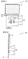
- Figure 5 is a plan view of such a COF LCD module.
- Figure 6 is a side view of the COF LCD module.
- a “sealing resin” herein means a resin which fills between an LC-driving IC and a flexible substrate so as to protect a contact between the LC-driving IC and the flexible substrate.
- a COF LCD module 400 includes an LCD element 8 and a COF 300 .
- the COF 300 includes a flexible substrate 9 on which an LC-driving IC 1 and a chip 10 are mounted.
- the flexible substrate 9 is, for example, fabricated in the following way.
- a copper foil having a thickness of about 2 to 35 ⁇ m is coated with a precursor of polyimide which is in turn cured.
- the resultant polyimide film substrate has a thickness of about 10 to 100 ⁇ m.
- Such a fabricating method is called casting.
- the substrate is etched to obtain the desired conductor pattern.
- the substrate is coated with a polyimide resin or an epoxy resin, except for portions of the substrate 9 on which the LC-driving IC 1 and the chip 10 and contacts of the LCD element 8 with the LC-driving IC 1 and the chip 10 .
- the conductor pattern on which a conductor is exposed is plated with Sn, Ni, Au, or the like. In this way, the flexible substrate 9 is fabricated.
- an additive method may be employed.
- a sputtered copper is patterned and then thickened by plating.
- the COF 300 is, for example, fabricated in the following way.
- the LC-driving IC 1 and the chip 10 are mounted on the conductor pattern of the flexible substrate 9 .
- the LC-driving IC 1 is implemented by flip chip bonding.
- the LC-driving IC 1 includes an Au bump (not shown) which is coupled with the conductor pattern.
- an Au bump (not shown) which is coupled with the conductor pattern.
- an Sn-Au alloy coupling method, or a coupling method using an anisotropic conductive film may be adopted.
- the Sn-Au alloy coupling method is performed in the following way.
- the LC-driving IC 1 is provided on the flexible substrate 9 so that the Au bump of the LC-driving IC 1 contacts with the Sn-plated conductor pattern.
- the Au bump is coupled with the conductor pattern by heating and pressing the flexible substrate 9 from the rear side thereof ( 9A side). Subsequently, the LC-driving IC 1 is sealed by a sealing resin 4 .
- the coupling method using an anisotropic conductive film is performed in the following way.
- the anisotropic conductive film is interposed between the flexible substrate 9 and the LC-driving IC 1 .
- the flexible substrate 9 is heated and pressed from the rear side thereof ( 9A side) so that the Au bump is electrically coupled with the conductor pattern while the Au bump is fixed on the conductor pattern by the cured anisotropic conductive film.
- the COF 300 fabricated as described above is conductive-coupled with the LCD element 8 using an anisotropic conductive film or the like, thereby obtaining the LCD module 400 .
- the Au bump is used as the segment output terminal of the LC-driving IC 1 .
- the coupling strength between the LC-driving IC 1 and the flexible substrate 9 needs to be enhanced and the COF 300 on which the LC-driving IC 1 is mounted needs to be thinner.
- the inventors fabricated and studied a prototype of the COF 300 , in which the LC-driving IC 1 having an Au bump having a narrower pitch, is mounted on the flexible substrate 9 by the Sn-Au alloy coupling.
- the Au migration is generated by an electric field being applied to a halogen and moisture.
- the document WO 98 20542 A corresponding to EP 0 957 513 , describes an electronic component part device having a packaging substrate and at least one electronic component part mounted on the packaging substrate wherein a bump electrode and the packaging substrate are connected through an adhesive film.
- the adhesive film is used to reduce heat stress at the time of heat cycling and to reduce undulation of electrode surfaces to increase the connection reliability.
- the adhesive film may contain thermosetting resin, epoxy resin or imide resin.
- the adhesive has a storage elastic modulus at 40°C after bonding, of from 100 to 4,000 MPa, while the in the preferred embodiments the elastic modulus is 1,200 MPa and 1,500 MPa, respectively.
- the document US-A-5 959 363 relates to a semiconductor device with a semiconductor chip being mounted on a circuit board through a bump electrode, and it discloses the use of two different encapsulation resins, one first resin disposed within an inner surrounded by the electrode connections and one second resin disposed in an outer region disposed beyond the leads positioned on the outermost periphery of the semiconductor device.
- the purpose of the use of the two different resins is to alleviate stress distortion.
- the resin may contain epoxy resin such as a bisphenol type epoxy resin or polyimide resin.
- the two different encapsulation resins contain a filler, the fillers having different particle diameters and different particle contents in each of the two resins.
- the preferred elastic modulus of the first resin is selected to be 900x10 7 Pa and the preferred elastic modulus of the second resin is selected to be 1200x10 7 Pa.
- the document US-A-5 916 688 discloses resin solutions having improved curing temperatures and improved solvent solubility.
- the resin may contain polyimide resin composed of aromatic tetra carboxylic acids and aromatic diamines.
- the resin solutions have a low elastic modulus.
- EP-A-0 422 906 discloses an LCD device comprising electrodes mounted on a substrate and is concerned with a connection resistance of semiconductor devices mounted on substrates.
- EP-A-0 303 256 discloses an electrode and a substrate connected through an electroconductive adhesive resin.
- the adhesive resin is suitable for easy removal from a glass substrate.
- a sealed-by-resin type semiconductor device includes: a substrate; a lead provided on the substrate; and a semiconductor element provided on the lead by flip chip bonding; wherein the semiconductor element includes a plurality of terminals connected to the lead, and wherein the plurality of terminals include an Au bump; the sealed-by-resin type semiconductor device further includes a resin for protecting the plurality of terminals; and the device being characterized in that the resin has a sufficiently low elasticity modulus that occurrence of undesirable migration is suppressed and the resin has a sufficiently high elasticity modulus that a coupling strength between the substrate and the semiconductor is sufficient, wherein the elasticity modulus is at least 0.3 GPa and at most 1 GPa.
- the resin includes a thermosetting resin, an epoxy resin, or a denatured polyimide resin.
- the resin includes an epoxy resin and the epoxy resin includes a bisphenol resin.
- the resin includes a denatured polyimide resin and the denatured polyimide resin includes aromatic tetracarboxylic acid and aromatic diamine.
- a pitch of the plurality of terminals is at most 70 ⁇ m.
- a liquid crystal display element is coupled with the substrate to form a liquid crystal display module.
- the liquid crystal display module further includes an anisotropic conductive film for coupling the substrate with the liquid crystal display element.
- the inventors conducted an experiment in which an Au bump to which a halogen compound was attached was exposed to high temperature and high humidity. As a result, occurrence of migration was suppressed and a sufficient coupling strength was obtained between the LC-driving IC 1 and the flexible substrate 9 when the elasticity modulus of the sealing resin 4 sealing the LC-driving IC 1 was optimized. This led to achievement of the present invention.
- the electrical coupling reliability of the semiconductor elements and the flexible circuit substrate such as heat-impact resistance, moisture resistance, and a coupling strength can be enhanced.
- An epoxy resin or a denatured polyimide resin is used as the sealing resin.
- the invention described herein makes possible the advantages of (1) providing a sealed-by-resin type semiconductor device capable of suppressing migration between Au bumps, and an LCD module including the same and (2) providing a sealed-by-resin type semiconductor device having a sufficient coupling strength between an LC-driving IC and a flexible substrate.
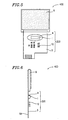
- Figure 1 is a plan view of a COF LCD module 200 according to an embodiment of the present invention.
- Figure 2 is a side view of a COF LCD module 200 according to the embodiment of the present invention.
- the same components as those included in the COF LCD module 400 are indicated by the same reference numerals as those used for the COF LCD module 400 . Detailed description is omitted for those components.
- the COF LCD module 200 includes an LCD element 8 and a COF 100 .
- the COF 100 includes a flexible substrate 9 on which an LC-driving IC 1 and a chip 10 are mounted.
- the COF LCD module 200 according to the embodiment of the present invention is different from the foregoing COF LCD module 400 in that in the COF LCD module 200 the LC-driving IC 1 is sealed by a sealing resin 12 , of which the elasticity modulus is optimized, instead of the sealing resin 4 .
- Figure 3 is a cross-sectional view of a major portion of the COF 100 according to the embodiment of the present invention.
- the sealing resin 12 seals the LC-driving IC 1 .
- a given electronic circuit (not shown) and an electrode pad 1B are provided on a rear side 1A of the LC-driving IC 1 .
- the Au bump 3 is provided on the electrode pad 1B .
- the outer dimensions of the LC-driving IC 1 are about 2 mm ⁇ 20 mm.
- the bump height H is about 15 ⁇ m.
- the minimum bump pitch P of the Au bump 3 is about 80 ⁇ m.
- the flexible substrate 9 includes a polyimide film 2 having a thickness of about 20 to 30 ⁇ m, a conductor pattern 5 of Cu provided on the polyimide film 2 , a portion on which the LC-driving IC 1 is mounted, a portion on which the chip 10 is mounted, an ink coverlay 6 of polyimide covering portions other than a connecting terminal 9A which connects an LCD element 8 and the COF 100 , an Sn plating layer 7 with which the conductor pattern 5 is coated.
- the flexible substrate 9 and the LC-driving IC 1 are registered so that the conductor pattern 5 is opposed to the Au bump 3 .
- the LC-driving IC 1 is heated and pressed from the top side thereof (in the direction indicated by arrow A) so as to couple the conductor patterns with the Au bump 3 due to an Sn-Au alloyed junction.
- the heating temperature is about 280°C or more which is sufficient so that the Sn plating layer 7 and the Au bump 3 form into an eutectic alloy.
- a sealing resin 12 is injected into a gap between the LC-driving IC 1 and the flexible substrate 9 .
- the sealing resin 12 is cured to seal the gap.
- the sealing resin 12 has an elasticity modulus which is sufficiently low so as not to generate undesirable migration.
- a resin is applied to the LC-driving IC 1 using a dispenser.
- the resin is heated for about two hours at about 100°C and then for about one hour at about 150°C so as to be cured.
- a transparent electrode connecting terminal 8A of the LCD element 8 is electrically coupled with a connecting terminal 9A of the flexible substrate 9 via an anisotropic conductive film.
- the LCD module 200 is completely fabricated.
- Example 1 a bisphenol type epoxy resin was used as the sealing resin.
- the elasticity modulus was measured by a dynamic viscoelasticity method (conducted at a room temperature of about 25°C).
- LCD modules were fabricated for each of the four types of bisphenol type epoxy resins having elasticity modulus of 0.005 GPa, 0.07 GPa, 0.3 GPa, and 1.0 GPa, respectively. All the LCD modules were placed in a moisture-resistance reliability test bath having a temerature of about 60°C and a humidity of about 95%. The rate of occurrence of an LCD abnormality, which is caused by leakage between the Au bumps due to the migration, was evaluated after about 1000 hours had passed.
- Figure 4 is a graph showing the rate of occurrence of the LCD abnormality that is caused by leakage between the Au bumps due to the migration, in Example 1. As is seen from Figure 4 , when the bisphenol type epoxy resin was used as the sealing resin 12 in Example 1, there were substantially no LCD abnormality that is caused by leakage between the Au bumps due to the migration.
- the coupling strength between the LC-driving IC 1 and the flexible substrate 9 was evaluated.
- the flexible substrate 9 was bent into a 90° angle while the LC-driving IC 1 was fixed on the flexible substrate 9 .
- a load was increasingly imposed on the LC-driving IC 1 while the LCD element 8 was displaying. In this case, the value of the load, which starts to generate the display abnormality in the LCD element 8 , was determined.
- the inventors' previous study has found that when the value of the load, which starts to generate the display abnormality in the LCD element 8 , is about 500 gf or more, there are substantially no adverse problems in the process of incorporating the COF LCD module into a device.
- Table 1 shows the values of loads which start to generate the display abnormality in the LCD elements having the respective elasticity.
- Table 1 Example 1 ( epoxy)
- Example 2 polyimide)
- Conventional example 1 epoxy
- Conventional example 2 Silicone
- Average value gf) 380 730 1220 1380 950 970 1510 1500 210
- Minimum value (gf) 350 690 1080 1100 880 860 1330 1350 180
- the values of loads are 500 gf or more.
- the epoxy resins used in Example 1 have shorter cure time, thereby improving productivity.
- Example 2 a denatured polyimide including aromatic tetracarboxylic acid and aromatic diamine was used as the sealing resin. Two types of the denatured polyimide having elasticity modulus of 0.45 GPa and 0.65 GPa, respectively. The elasticity modulus was measured by the dynamic viscoelasticity method, similar to Example 1 (conducted at a room temperature of about 25°C).
- COF LCD modules 200 were fabricated for each of the two types of the denatured polyimide having elasticity modulus of 0.45 GPa and 0.65 GPa, respectively, in a way similar to Example 1.
- the sealing resin was heated for two hours at 90°C and then for two hours at 150°C.
- the coupling strength between the LC-driving IC 1 and the flexible substrate 9 was evaluated in a way similar to that of Example 1 and the results are shown in Table 1.
- the obtained values of loads are 500 gf or more.
- the denatured polyimide having elasticity modulus of 0.07 GPa or more and 1 GPa or less has the same effect as that of Example 1.
- Example 1 In Conventional Example 1, two types of epoxy resins having elasticity modulus of 2.5 GPa and 3.1 Gpa, which are higher than the elasticity modulus of the sealing resins of Examples 1 and 2, were used.
- Example 2 Similar to Example 1, 50 COF LCD modules were fabricated for each elasticity modulus. The sealing resins were cured for two hours at 120°C and then for two hours at 150°C. All the COF LCD modules were subjected to a moisture-resistance reliability test similar to that of Example 1.
- Example 2 a silicone resin having an elasticity modulus of 0.0006 GPa, which is lower than the elasticity modulus of the sealing resins of Examples 1 and 2, was used.
- Example 2 Similar to Example 1, 50 COF LCD modules were fabricated. The sealing resin was cured for four hours at 150°C. The COF LCD modules were subjected to a moisture-resistance reliability test similar to that of Example 1.
- the present invention can provide the sealed-by-resin type semiconductor device capable of suppressing occurrence of migration between the Au bumps, and an LCD module including the same.
- the present invention can provide the sealed-by-resin type semiconductor device having a sufficient coupling strength between the LC-driving IC and the flexible substrate, and an LCD module including the same.
- the epoxy resin or denatured polyimide resin having an elasticity modulus of 0.07 GPa or more and 1 GPa or less is used as a sealing resin protecting semiconductor elements. Therefore, it is possible to suppress occurrence of migration which is responsible for the leakage between the Au bumps. Moreover, a coupling strength between the semiconductor elements and the flexible substrate is sufficient, which is an excellent, characteristic effect.
Landscapes
- Engineering & Computer Science (AREA)
- Microelectronics & Electronic Packaging (AREA)
- Condensed Matter Physics & Semiconductors (AREA)
- General Physics & Mathematics (AREA)
- Computer Hardware Design (AREA)
- Physics & Mathematics (AREA)
- Power Engineering (AREA)
- Manufacturing & Machinery (AREA)
- Wire Bonding (AREA)
- Structures Or Materials For Encapsulating Or Coating Semiconductor Devices Or Solid State Devices (AREA)
- Liquid Crystal (AREA)
- Devices For Indicating Variable Information By Combining Individual Elements (AREA)
- Structures For Mounting Electric Components On Printed Circuit Boards (AREA)
- Encapsulation Of And Coatings For Semiconductor Or Solid State Devices (AREA)
Claims (7)
- Dispositif à semi-conducteur du type scellé par une résine, comprenant :un substrat ;un conducteur prévu sur le substrat ; etun élément semi-conducteur prévu sur le conducteur par connexion par billes ;dans lequel l'élément semi-conducteur comprend une pluralité de bornes reliées au conducteur, et dans lequel la pluralité de bornes comprend un bossage en Au ;le dispositif semi-conducteur du type scellé par une résine comprend en outre une résine pour protéger la pluralité de bornes; etdans lequella résine possède un module d'élasticité suffisamment faible pour que l'apparition d'une migration non désirée soit supprimée et la résine a un module d'élasticité suffisamment élevé pour qu'une force de couplage entre le substrat et le semi-conducteur soit suffisante, le module d'élasticité étant d'au moins 0,3 GPa et d'au plus 1 GPa.
- Dispositif semi-conducteur du type scellé par une résine selon la revendication 1, dans lequel la résine comprend une résine thermodurcissable, une résine époxy, ou une résine de polyimide dénaturé.
- Dispositif semi-conducteur du type scellé par une résine selon la revendication 2, dans lequel la résine comprend une résine époxy et la résine époxy comprend une résine de bisphénol.
- Dispositif semi-conducteur du type scellé par une résine selon la revendication 2, dans lequel la résine comprend une résine de polyimide dénaturé et la résine de polyimide dénaturé comprend un acide tétracarboxylique aromatique et une diamine aromatique.
- Dispositif semi-conducteur du type scellé par une résine selon la revendication 1, dans lequel le pas de la pluralité de bornes est d'au plus 70 µm.
- Dispositif semi-conducteur du type scellé par une résine selon la revendication 1, dans lequel un élément d'affichage à cristaux liquides est couplé avec le substrat pour former un module d'affichage à cristaux liquides.
- Dispositif semi-conducteur du type scellé par une résine selon la revendication 6, comprenant en outre un film conducteur anisotrope pour coupler le substrat à l'élément d'affichage à cristaux liquides.
Applications Claiming Priority (2)
| Application Number | Priority Date | Filing Date | Title |
|---|---|---|---|
| JP31043299 | 1999-10-29 | ||
| JP31043299A JP3441412B2 (ja) | 1999-10-29 | 1999-10-29 | 樹脂封止型半導体装置およびこれを用いた液晶表示モジュール |
Publications (3)
| Publication Number | Publication Date |
|---|---|
| EP1096565A2 EP1096565A2 (fr) | 2001-05-02 |
| EP1096565A3 EP1096565A3 (fr) | 2003-01-08 |
| EP1096565B1 true EP1096565B1 (fr) | 2007-12-12 |
Family
ID=18005186
Family Applications (1)
| Application Number | Title | Priority Date | Filing Date |
|---|---|---|---|
| EP00123049A Expired - Lifetime EP1096565B1 (fr) | 1999-10-29 | 2000-10-24 | Dispositif semiconducteur scellé par une résine et module d'affichage à cristaux liquides comprenant le dit dispositif |
Country Status (7)
| Country | Link |
|---|---|
| US (1) | US6388339B1 (fr) |
| EP (1) | EP1096565B1 (fr) |
| JP (1) | JP3441412B2 (fr) |
| KR (1) | KR20010060214A (fr) |
| CN (1) | CN1199253C (fr) |
| DE (1) | DE60037383T2 (fr) |
| TW (1) | TW495947B (fr) |
Families Citing this family (19)
| Publication number | Priority date | Publication date | Assignee | Title |
|---|---|---|---|---|
| JP4002112B2 (ja) * | 2001-03-22 | 2007-10-31 | シチズンホールディングス株式会社 | 液晶表示装置 |
| JP4880838B2 (ja) * | 2001-09-05 | 2012-02-22 | 株式会社東芝 | 液晶表示装置の組立て方法及び組立て装置 |
| US6969914B2 (en) | 2002-08-29 | 2005-11-29 | Micron Technology, Inc. | Electronic device package |
| JP2004327920A (ja) * | 2003-04-28 | 2004-11-18 | Sharp Corp | 半導体装置の製造方法、フレキシブル基板及び半導体装置 |
| US7646095B2 (en) | 2003-09-30 | 2010-01-12 | Panasonic Corporation | Semiconductor device |
| KR101075599B1 (ko) * | 2004-06-23 | 2011-10-20 | 삼성전자주식회사 | 표시장치 |
| JP2006216720A (ja) | 2005-02-02 | 2006-08-17 | Sharp Corp | 半導体装置及びその製造方法 |
| KR101119153B1 (ko) * | 2005-02-07 | 2012-03-19 | 삼성전자주식회사 | 표시장치 |
| JP5057321B2 (ja) | 2006-03-14 | 2012-10-24 | 株式会社ジャパンディスプレイウェスト | 表示装置の製造方法 |
| JP5014945B2 (ja) * | 2007-10-17 | 2012-08-29 | シャープ株式会社 | 半導体装置 |
| TWI400509B (zh) * | 2008-06-13 | 2013-07-01 | Prime View Int Co Ltd | 可撓性顯示模組及其製作方法 |
| TWI476738B (zh) * | 2010-09-07 | 2015-03-11 | Ind Tech Res Inst | 軟性顯示面板及其組裝方法 |
| WO2012067003A1 (fr) * | 2010-11-17 | 2012-05-24 | シャープ株式会社 | Substrat de circuit et procédé de fabrication de celui-ci |
| JP5296116B2 (ja) * | 2011-02-16 | 2013-09-25 | シャープ株式会社 | 半導体装置 |
| JP6055275B2 (ja) * | 2012-11-05 | 2016-12-27 | ローム株式会社 | 半導体集積回路装置および電子機器 |
| JP6478449B2 (ja) * | 2013-08-21 | 2019-03-06 | キヤノン株式会社 | 装置の製造方法及び機器の製造方法 |
| JP6519112B2 (ja) * | 2014-07-24 | 2019-05-29 | Tdk株式会社 | 薄膜キャパシタ |
| CN109897599B (zh) * | 2015-11-09 | 2020-09-01 | 积水化学工业株式会社 | 液晶显示元件用密封剂、上下导通材料和液晶显示元件 |
| CN112909062B (zh) * | 2021-02-03 | 2024-03-15 | 京东方科技集团股份有限公司 | 一种显示模组的制备方法 |
Family Cites Families (14)
| Publication number | Priority date | Publication date | Assignee | Title |
|---|---|---|---|---|
| JPS60238817A (ja) * | 1984-05-12 | 1985-11-27 | Citizen Watch Co Ltd | 液晶表示装置 |
| US4917466A (en) * | 1987-08-13 | 1990-04-17 | Shin-Etsu Polymer Co., Ltd. | Method for electrically connecting IC chips, a resinous bump-forming composition used therein and a liquid-crystal display unit electrically connected thereby |
| JPH0193155A (ja) | 1987-10-05 | 1989-04-12 | Sumitomo Bakelite Co Ltd | 樹脂封止型半導体装置 |
| JPH03125443A (ja) * | 1989-10-09 | 1991-05-28 | Sharp Corp | 実装基板の電極及び該実装基板の電極を有する液晶表示装置 |
| JPH06236899A (ja) | 1992-09-29 | 1994-08-23 | Toshiba Corp | 樹脂封止型半導体装置 |
| JPH06224239A (ja) | 1993-01-21 | 1994-08-12 | Toshiba Corp | 樹脂封止型半導体装置の製造方法 |
| JPH0897334A (ja) | 1994-09-29 | 1996-04-12 | Hitachi Ltd | 樹脂封止型半導体装置 |
| US5864178A (en) * | 1995-01-12 | 1999-01-26 | Kabushiki Kaisha Toshiba | Semiconductor device with improved encapsulating resin |
| JP3284262B2 (ja) * | 1996-09-05 | 2002-05-20 | セイコーエプソン株式会社 | 液晶表示装置及びそれを用いた電子機器 |
| KR100603484B1 (ko) * | 1996-10-08 | 2006-07-24 | 히다치 가세고교 가부시끼가이샤 | 접착제 및 양면 접착 필름 |
| TW383435B (en) * | 1996-11-01 | 2000-03-01 | Hitachi Chemical Co Ltd | Electronic device |
| JP3689518B2 (ja) * | 1997-02-18 | 2005-08-31 | 新日鐵化学株式会社 | 電子材料用樹脂溶液組成物 |
| TW459032B (en) * | 1998-03-18 | 2001-10-11 | Sumitomo Bakelite Co | An anisotropic conductive adhesive and method for preparation thereof and an electronic apparatus using said adhesive |
| US6108210A (en) * | 1998-04-24 | 2000-08-22 | Amerasia International Technology, Inc. | Flip chip devices with flexible conductive adhesive |
-
1999
- 1999-10-29 JP JP31043299A patent/JP3441412B2/ja not_active Expired - Fee Related
-
2000
- 2000-10-04 TW TW089120664A patent/TW495947B/zh not_active IP Right Cessation
- 2000-10-24 DE DE60037383T patent/DE60037383T2/de not_active Expired - Lifetime
- 2000-10-24 EP EP00123049A patent/EP1096565B1/fr not_active Expired - Lifetime
- 2000-10-26 CN CNB001319833A patent/CN1199253C/zh not_active Expired - Fee Related
- 2000-10-27 US US09/697,599 patent/US6388339B1/en not_active Expired - Fee Related
- 2000-10-28 KR KR1020000063706A patent/KR20010060214A/ko not_active Application Discontinuation
Also Published As
| Publication number | Publication date |
|---|---|
| CN1303086A (zh) | 2001-07-11 |
| JP3441412B2 (ja) | 2003-09-02 |
| DE60037383D1 (de) | 2008-01-24 |
| US6388339B1 (en) | 2002-05-14 |
| JP2001127216A (ja) | 2001-05-11 |
| CN1199253C (zh) | 2005-04-27 |
| EP1096565A3 (fr) | 2003-01-08 |
| EP1096565A2 (fr) | 2001-05-02 |
| TW495947B (en) | 2002-07-21 |
| KR20010060214A (ko) | 2001-07-06 |
| DE60037383T2 (de) | 2008-12-04 |
Similar Documents
| Publication | Publication Date | Title |
|---|---|---|
| EP1096565B1 (fr) | Dispositif semiconducteur scellé par une résine et module d'affichage à cristaux liquides comprenant le dit dispositif | |
| KR100408616B1 (ko) | 반도체 장치, 전자 기기의 제조 방법, 전자 기기 및 휴대정보 단말 | |
| US5949142A (en) | Chip size package and method of manufacturing the same | |
| KR100324708B1 (ko) | 반도체장치 | |
| US7180007B2 (en) | Electronic circuit device and its manufacturing method | |
| GB2286084A (en) | Electronic package with thermally conductive support | |
| US20020079594A1 (en) | Semiconductor device and method of manufacture thereof, circuit board, and electronic instrument | |
| JP2001217354A (ja) | 半導体チップの実装構造、および半導体装置 | |
| US6528889B1 (en) | Electronic circuit device having adhesion-reinforcing pattern on a circuit board for flip-chip mounting an IC chip | |
| KR20050021905A (ko) | 반도체 장치용 패키지 | |
| JP2000243864A (ja) | 半導体装置及びその製造方法、回路基板並びに電子機器 | |
| JP3116926B2 (ja) | パッケージ構造並びに半導体装置、パッケージ製造方法及び半導体装置製造方法 | |
| US6434817B1 (en) | Method for joining an integrated circuit | |
| JP2002289735A (ja) | 半導体装置 | |
| JP2967080B1 (ja) | 半導体装置の実装体の製造方法 | |
| JP4699089B2 (ja) | チップオンフィルム半導体装置 | |
| KR100833937B1 (ko) | 이방성 도전 접착제 | |
| JP2705658B2 (ja) | 電子デバイス組立体およびその製造方法 | |
| KR100310037B1 (ko) | 복수개의집적회로칩을연성인쇄회로기판상에실장히기위한방법 | |
| JP4374251B2 (ja) | 半導体装置 | |
| JP3099767B2 (ja) | 電子部品組立体およびその製造方法 | |
| JP2947213B2 (ja) | 電子部品組立体およびその製造方法 | |
| JP2000022045A (ja) | 半導体装置 | |
| JPH11154718A (ja) | 半導体装置 | |
| JPH0730056A (ja) | マルチチップモジュール実装型プリント配線板 |
Legal Events
| Date | Code | Title | Description |
|---|---|---|---|
| PUAI | Public reference made under article 153(3) epc to a published international application that has entered the european phase |
Free format text: ORIGINAL CODE: 0009012 |
|
| AK | Designated contracting states |
Kind code of ref document: A2 Designated state(s): AT BE CH CY DE DK ES FI FR GB GR IE IT LI LU MC NL PT SE |
|
| AX | Request for extension of the european patent |
Free format text: AL;LT;LV;MK;RO;SI |
|
| PUAL | Search report despatched |
Free format text: ORIGINAL CODE: 0009013 |
|
| AK | Designated contracting states |
Kind code of ref document: A3 Designated state(s): AT BE CH CY DE DK ES FI FR GB GR IE IT LI LU MC NL PT SE |
|
| AX | Request for extension of the european patent |
Free format text: AL;LT;LV;MK;RO;SI |
|
| RIC1 | Information provided on ipc code assigned before grant |
Free format text: 7H 01L 23/29 A, 7H 01L 21/56 B |
|
| 17P | Request for examination filed |
Effective date: 20030508 |
|
| AKX | Designation fees paid |
Designated state(s): DE FR GB |
|
| 17Q | First examination report despatched |
Effective date: 20030930 |
|
| GRAP | Despatch of communication of intention to grant a patent |
Free format text: ORIGINAL CODE: EPIDOSNIGR1 |
|
| GRAS | Grant fee paid |
Free format text: ORIGINAL CODE: EPIDOSNIGR3 |
|
| GRAA | (expected) grant |
Free format text: ORIGINAL CODE: 0009210 |
|
| AK | Designated contracting states |
Kind code of ref document: B1 Designated state(s): DE FR GB |
|
| REG | Reference to a national code |
Ref country code: GB Ref legal event code: FG4D |
|
| REF | Corresponds to: |
Ref document number: 60037383 Country of ref document: DE Date of ref document: 20080124 Kind code of ref document: P |
|
| ET | Fr: translation filed | ||
| PLBE | No opposition filed within time limit |
Free format text: ORIGINAL CODE: 0009261 |
|
| STAA | Information on the status of an ep patent application or granted ep patent |
Free format text: STATUS: NO OPPOSITION FILED WITHIN TIME LIMIT |
|
| 26N | No opposition filed |
Effective date: 20080915 |
|
| PGFP | Annual fee paid to national office [announced via postgrant information from national office to epo] |
Ref country code: FR Payment date: 20121018 Year of fee payment: 13 Ref country code: DE Payment date: 20121017 Year of fee payment: 13 |
|
| PGFP | Annual fee paid to national office [announced via postgrant information from national office to epo] |
Ref country code: GB Payment date: 20121024 Year of fee payment: 13 |
|
| GBPC | Gb: european patent ceased through non-payment of renewal fee |
Effective date: 20131024 |
|
| PG25 | Lapsed in a contracting state [announced via postgrant information from national office to epo] |
Ref country code: GB Free format text: LAPSE BECAUSE OF NON-PAYMENT OF DUE FEES Effective date: 20131024 |
|
| REG | Reference to a national code |
Ref country code: DE Ref legal event code: R119 Ref document number: 60037383 Country of ref document: DE Effective date: 20140501 |
|
| REG | Reference to a national code |
Ref country code: FR Ref legal event code: ST Effective date: 20140630 |
|
| PG25 | Lapsed in a contracting state [announced via postgrant information from national office to epo] |
Ref country code: DE Free format text: LAPSE BECAUSE OF NON-PAYMENT OF DUE FEES Effective date: 20140501 Ref country code: FR Free format text: LAPSE BECAUSE OF NON-PAYMENT OF DUE FEES Effective date: 20131031 |