EP1089338A2 - CMOS Schaltkreis aus GaAs/Ge auf Si Substrat - Google Patents
CMOS Schaltkreis aus GaAs/Ge auf Si Substrat Download PDFInfo
- Publication number
- EP1089338A2 EP1089338A2 EP00305875A EP00305875A EP1089338A2 EP 1089338 A2 EP1089338 A2 EP 1089338A2 EP 00305875 A EP00305875 A EP 00305875A EP 00305875 A EP00305875 A EP 00305875A EP 1089338 A2 EP1089338 A2 EP 1089338A2
- Authority
- EP
- European Patent Office
- Prior art keywords
- region
- gallium arsenide
- substrate
- germanium
- forming
- Prior art date
- Legal status (The legal status is an assumption and is not a legal conclusion. Google has not performed a legal analysis and makes no representation as to the accuracy of the status listed.)
- Withdrawn
Links
Images
Classifications
-
- H—ELECTRICITY
- H10—SEMICONDUCTOR DEVICES; ELECTRIC SOLID-STATE DEVICES NOT OTHERWISE PROVIDED FOR
- H10D—INORGANIC ELECTRIC SEMICONDUCTOR DEVICES
- H10D84/00—Integrated devices formed in or on semiconductor substrates that comprise only semiconducting layers, e.g. on Si wafers or on GaAs-on-Si wafers
- H10D84/01—Manufacture or treatment
-
- H—ELECTRICITY
- H10—SEMICONDUCTOR DEVICES; ELECTRIC SOLID-STATE DEVICES NOT OTHERWISE PROVIDED FOR
- H10D—INORGANIC ELECTRIC SEMICONDUCTOR DEVICES
- H10D84/00—Integrated devices formed in or on semiconductor substrates that comprise only semiconducting layers, e.g. on Si wafers or on GaAs-on-Si wafers
- H10D84/01—Manufacture or treatment
- H10D84/02—Manufacture or treatment characterised by using material-based technologies
- H10D84/08—Manufacture or treatment characterised by using material-based technologies using combinations of technologies, e.g. using both Si and SiC technologies or using both Si and Group III-V technologies
-
- H—ELECTRICITY
- H10—SEMICONDUCTOR DEVICES; ELECTRIC SOLID-STATE DEVICES NOT OTHERWISE PROVIDED FOR
- H10D—INORGANIC ELECTRIC SEMICONDUCTOR DEVICES
- H10D84/00—Integrated devices formed in or on semiconductor substrates that comprise only semiconducting layers, e.g. on Si wafers or on GaAs-on-Si wafers
- H10D84/80—Integrated devices formed in or on semiconductor substrates that comprise only semiconducting layers, e.g. on Si wafers or on GaAs-on-Si wafers characterised by the integration of at least one component covered by groups H10D12/00 or H10D30/00, e.g. integration of IGFETs
- H10D84/82—Integrated devices formed in or on semiconductor substrates that comprise only semiconducting layers, e.g. on Si wafers or on GaAs-on-Si wafers characterised by the integration of at least one component covered by groups H10D12/00 or H10D30/00, e.g. integration of IGFETs of only field-effect components
- H10D84/83—Integrated devices formed in or on semiconductor substrates that comprise only semiconducting layers, e.g. on Si wafers or on GaAs-on-Si wafers characterised by the integration of at least one component covered by groups H10D12/00 or H10D30/00, e.g. integration of IGFETs of only field-effect components of only insulated-gate FETs [IGFET]
- H10D84/85—Complementary IGFETs, e.g. CMOS
-
- H—ELECTRICITY
- H10—SEMICONDUCTOR DEVICES; ELECTRIC SOLID-STATE DEVICES NOT OTHERWISE PROVIDED FOR
- H10D—INORGANIC ELECTRIC SEMICONDUCTOR DEVICES
- H10D84/00—Integrated devices formed in or on semiconductor substrates that comprise only semiconducting layers, e.g. on Si wafers or on GaAs-on-Si wafers
- H10D84/01—Manufacture or treatment
- H10D84/0123—Integrating together multiple components covered by H10D12/00 or H10D30/00, e.g. integrating multiple IGBTs
- H10D84/0126—Integrating together multiple components covered by H10D12/00 or H10D30/00, e.g. integrating multiple IGBTs the components including insulated gates, e.g. IGFETs
- H10D84/0165—Integrating together multiple components covered by H10D12/00 or H10D30/00, e.g. integrating multiple IGBTs the components including insulated gates, e.g. IGFETs the components including complementary IGFETs, e.g. CMOS devices
- H10D84/0167—Manufacturing their channels
-
- H—ELECTRICITY
- H10—SEMICONDUCTOR DEVICES; ELECTRIC SOLID-STATE DEVICES NOT OTHERWISE PROVIDED FOR
- H10D—INORGANIC ELECTRIC SEMICONDUCTOR DEVICES
- H10D84/00—Integrated devices formed in or on semiconductor substrates that comprise only semiconducting layers, e.g. on Si wafers or on GaAs-on-Si wafers
- H10D84/01—Manufacture or treatment
- H10D84/02—Manufacture or treatment characterised by using material-based technologies
- H10D84/03—Manufacture or treatment characterised by using material-based technologies using Group IV technology, e.g. silicon technology or silicon-carbide [SiC] technology
- H10D84/038—Manufacture or treatment characterised by using material-based technologies using Group IV technology, e.g. silicon technology or silicon-carbide [SiC] technology using silicon technology, e.g. SiGe
-
- Y—GENERAL TAGGING OF NEW TECHNOLOGICAL DEVELOPMENTS; GENERAL TAGGING OF CROSS-SECTIONAL TECHNOLOGIES SPANNING OVER SEVERAL SECTIONS OF THE IPC; TECHNICAL SUBJECTS COVERED BY FORMER USPC CROSS-REFERENCE ART COLLECTIONS [XRACs] AND DIGESTS
- Y10—TECHNICAL SUBJECTS COVERED BY FORMER USPC
- Y10S—TECHNICAL SUBJECTS COVERED BY FORMER USPC CROSS-REFERENCE ART COLLECTIONS [XRACs] AND DIGESTS
- Y10S438/00—Semiconductor device manufacturing: process
- Y10S438/933—Germanium or silicon or Ge-Si on III-V
-
- Y—GENERAL TAGGING OF NEW TECHNOLOGICAL DEVELOPMENTS; GENERAL TAGGING OF CROSS-SECTIONAL TECHNOLOGIES SPANNING OVER SEVERAL SECTIONS OF THE IPC; TECHNICAL SUBJECTS COVERED BY FORMER USPC CROSS-REFERENCE ART COLLECTIONS [XRACs] AND DIGESTS
- Y10—TECHNICAL SUBJECTS COVERED BY FORMER USPC
- Y10S—TECHNICAL SUBJECTS COVERED BY FORMER USPC CROSS-REFERENCE ART COLLECTIONS [XRACs] AND DIGESTS
- Y10S438/00—Semiconductor device manufacturing: process
- Y10S438/935—Gas flow control
Definitions
- GaAs metal semiconductor field effect transistors MOSFETs
- CMOS complementary metal oxide semiconductor
- MOS SiGe/Si metal oxide semiconductor
- AlGaAs/Ge/GaAs HBTs GaAs MOS devices.
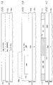
- a GaAs/Ge on Si CMOS integrated circuit is formed to improve transistor switching (propagation) delay by taking advantage of the high electron mobility for GaAs in the N-channel device and the high hole mobility for Ge in the P-channel device.
- a semi-insulating (undoped) layer of GaAs is formed over a silicon base to provide a buffer layer, significantly lessening the possibility of latch-up.
- GaAs and Ge wells are then formed over the semi-insulating GaAs layer, electrically isolated by standard thermal oxide and/or flowable oxide (HSQ).
- HSQ standard thermal oxide and/or flowable oxide
- N-channel MOS devices and P-channel MOS devices are formed in the GaAs and Ge wells, respectively, and interconnected to form the integrated circuit.
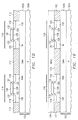
- any isolation oxide region 112 may optionally be a thermal oxide, a deposited oxide, or some other dielectric.
- the oxide may be grown after the formation of GaAs well 106 and Ge well 110 but before formation of an overlying FOX.
- a deposited oxide or other deposited dielectric region may be deposited after formation of GaAs and Ge wells 106 and 110 but before formation of an overlying FOX layer.
- Isolation oxide may be formed of any number of dielectric layers and materials between and around GaAs and Ge wells 106 and 110 .
- the combined thickness of such dielectric layers and materials is preferably less than the thickness of GaAs and Ge wells 106 and 110 , and a FOX layer is preferably formed over all such dielectric layers and materials as described above, then etched back until the upper surface of isolation regions 112 are substantially planar with the upper surfaces of GaAs and Ge wells 106 and 110 .
- NMOS device 114 includes a gate dielectric 126 .
- the gate dielectric 126 for NMOS device 114 is preferably gallium oxide (GaO x ), which may be thermally grown or deposited to a thickness selected for desired device performance.
- PMOS device 116 includes a gate dielectric 128 .
- the gate dielectric 128 for PMOS device 116 is preferably silicon dioxide (SiO 2 ), which may be formed by conventional methods (e.g., deposited) with a thickness selected for desired device performance.
- Gate electrodes 130 for both NMOS and PMOS devices 114 and 116 may be polysilicon, and sidewalls 132 for both devices may be conventional tetraethoxysilane (TEOS) dielectric sidewall structures or other appropriate materials.
- TEOS tetraethoxysilane
- a layer or several layers of insulation or passivation material 134 such as borophosphosilicate glass (BPSG) is formed over the devices 114 and 116 as depicted in Figure 1E , together with any other metallization, insulation, or passivation layers (not shown) which are required to form a complete integrated circuit.
- BPSG borophosphosilicate glass
- NMOS device 114 and one PMOS device 116 are shown in the exemplary embodiment as being formed within GaAs well 106 and Ge well 110 , those skilled in the art will recognize that GaAs well 106 and Ge well 110 are elongate, shown only in cross-section, and may contain any number of NMOS or PMOS devices. These devices may be connected by interconnects within various metallization levels to form any integrated circuit.
- the present invention reduces transistor propagation delay and improves integrated circuit speed by implementing CMOS circuits in a GaAs/Ge on Si structure, taking advantage of the electron mobility for GaAs and the hole mobility for Ge.
- a semi-insulating GaAs buffer layer between the silicon base of the substrate and the GaAs and Ge device wells substantially eliminates the possibility of latch-up.
- Flowable oxide or other insulating material between wells provides requisite lateral electrical isolation.
Landscapes
- Metal-Oxide And Bipolar Metal-Oxide Semiconductor Integrated Circuits (AREA)
- Element Separation (AREA)
- Formation Of Insulating Films (AREA)
- Insulated Gate Type Field-Effect Transistor (AREA)
Applications Claiming Priority (2)
| Application Number | Priority Date | Filing Date | Title |
|---|---|---|---|
| US09/363,214 US6563143B2 (en) | 1999-07-29 | 1999-07-29 | CMOS circuit of GaAs/Ge on Si substrate |
| US363214 | 1999-07-29 |
Publications (2)
| Publication Number | Publication Date |
|---|---|
| EP1089338A2 true EP1089338A2 (de) | 2001-04-04 |
| EP1089338A3 EP1089338A3 (de) | 2005-03-23 |
Family
ID=23429302
Family Applications (1)
| Application Number | Title | Priority Date | Filing Date |
|---|---|---|---|
| EP00305875A Withdrawn EP1089338A3 (de) | 1999-07-29 | 2000-07-12 | CMOS Schaltkreis aus GaAs/Ge auf Si Substrat |
Country Status (3)
| Country | Link |
|---|---|
| US (3) | US6563143B2 (de) |
| EP (1) | EP1089338A3 (de) |
| JP (1) | JP2001093987A (de) |
Cited By (10)
| Publication number | Priority date | Publication date | Assignee | Title |
|---|---|---|---|---|
| WO2003010805A3 (en) * | 2001-07-23 | 2003-09-18 | Motorola Inc | Complementary iii-v structures and devices |
| US6693298B2 (en) | 2001-07-20 | 2004-02-17 | Motorola, Inc. | Structure and method for fabricating epitaxial semiconductor on insulator (SOI) structures and devices utilizing the formation of a compliant substrate for materials used to form same |
| US6709989B2 (en) | 2001-06-21 | 2004-03-23 | Motorola, Inc. | Method for fabricating a semiconductor structure including a metal oxide interface with silicon |
| US6806202B2 (en) | 2002-12-03 | 2004-10-19 | Motorola, Inc. | Method of removing silicon oxide from a surface of a substrate |
| US6855992B2 (en) | 2001-07-24 | 2005-02-15 | Motorola Inc. | Structure and method for fabricating configurable transistor devices utilizing the formation of a compliant substrate for materials used to form the same |
| CN101606240B (zh) * | 2007-03-15 | 2014-03-12 | 英特尔公司 | 具有双外延沟道和自对准接点的cmos器件 |
| EP2333827A3 (de) * | 2009-12-10 | 2014-08-13 | International Rectifier Corporation | Monolithisches integriertes zusammengesetztes Halbleiterbauelement der Gruppe III-IV und Gruppe IV sowie Verfahren zu seiner Herstellung |
| KR20150028626A (ko) * | 2013-09-06 | 2015-03-16 | 삼성전자주식회사 | Cmos 소자 및 그 제조 방법 |
| EP2897161A1 (de) * | 2014-01-15 | 2015-07-22 | Imec | Verfahren zur Herstellung einer CMOS-Vorrichtung |
| KR20170017886A (ko) * | 2014-06-24 | 2017-02-15 | 인텔 코포레이션 | 동일 다이 상에 ge/sige 채널 및 iii-v 채널 트랜지스터를 형성하기 위한 기술 |
Families Citing this family (39)
| Publication number | Priority date | Publication date | Assignee | Title |
|---|---|---|---|---|
| US6392257B1 (en) | 2000-02-10 | 2002-05-21 | Motorola Inc. | Semiconductor structure, semiconductor device, communicating device, integrated circuit, and process for fabricating the same |
| AU2001257346A1 (en) | 2000-05-31 | 2001-12-11 | Motorola, Inc. | Semiconductor device and method for manufacturing the same |
| WO2002009187A2 (en) | 2000-07-24 | 2002-01-31 | Motorola, Inc. | Heterojunction tunneling diodes and process for fabricating same |
| US20020096683A1 (en) | 2001-01-19 | 2002-07-25 | Motorola, Inc. | Structure and method for fabricating GaN devices utilizing the formation of a compliant substrate |
| WO2002082551A1 (en) | 2001-04-02 | 2002-10-17 | Motorola, Inc. | A semiconductor structure exhibiting reduced leakage current |
| US6992321B2 (en) | 2001-07-13 | 2006-01-31 | Motorola, Inc. | Structure and method for fabricating semiconductor structures and devices utilizing piezoelectric materials |
| US7019332B2 (en) | 2001-07-20 | 2006-03-28 | Freescale Semiconductor, Inc. | Fabrication of a wavelength locker within a semiconductor structure |
| US20030034491A1 (en) | 2001-08-14 | 2003-02-20 | Motorola, Inc. | Structure and method for fabricating semiconductor structures and devices for detecting an object |
| US20030071327A1 (en) | 2001-10-17 | 2003-04-17 | Motorola, Inc. | Method and apparatus utilizing monocrystalline insulator |
| US20030132433A1 (en) * | 2002-01-15 | 2003-07-17 | Piner Edwin L. | Semiconductor structures including a gallium nitride material component and a silicon germanium component |
| US6916717B2 (en) | 2002-05-03 | 2005-07-12 | Motorola, Inc. | Method for growing a monocrystalline oxide layer and for fabricating a semiconductor device on a monocrystalline substrate |
| US7169619B2 (en) | 2002-11-19 | 2007-01-30 | Freescale Semiconductor, Inc. | Method for fabricating semiconductor structures on vicinal substrates using a low temperature, low pressure, alkaline earth metal-rich process |
| US6885065B2 (en) | 2002-11-20 | 2005-04-26 | Freescale Semiconductor, Inc. | Ferromagnetic semiconductor structure and method for forming the same |
| US6965128B2 (en) | 2003-02-03 | 2005-11-15 | Freescale Semiconductor, Inc. | Structure and method for fabricating semiconductor microresonator devices |
| US7095065B2 (en) * | 2003-08-05 | 2006-08-22 | Advanced Micro Devices, Inc. | Varying carrier mobility in semiconductor devices to achieve overall design goals |
| US7282425B2 (en) * | 2005-01-31 | 2007-10-16 | International Business Machines Corporation | Structure and method of integrating compound and elemental semiconductors for high-performance CMOS |
| US8866190B2 (en) * | 2005-06-14 | 2014-10-21 | International Rectifler Corporation | Methods of combining silicon and III-nitride material on a single wafer |
| US20070252216A1 (en) * | 2006-04-28 | 2007-11-01 | Infineon Technologies Ag | Semiconductor device and a method of manufacturing such a semiconductor device |
| US7791063B2 (en) * | 2007-08-30 | 2010-09-07 | Intel Corporation | High hole mobility p-channel Ge transistor structure on Si substrate |
| US7964487B2 (en) | 2008-06-04 | 2011-06-21 | International Business Machines Corporation | Carrier mobility enhanced channel devices and method of manufacture |
| US8524562B2 (en) * | 2008-09-16 | 2013-09-03 | Imec | Method for reducing Fermi-Level-Pinning in a non-silicon channel MOS device |
| WO2011056803A2 (en) * | 2009-11-06 | 2011-05-12 | Sony Corporation Of America | Stereoscopic overlay offset creation and editing |
| JP2011146691A (ja) | 2009-12-15 | 2011-07-28 | Sumitomo Chemical Co Ltd | 半導体基板、半導体デバイスおよび半導体基板の製造方法 |
| US8912055B2 (en) | 2011-05-03 | 2014-12-16 | Imec | Method for manufacturing a hybrid MOSFET device and hybrid MOSFET obtainable thereby |
| TW201306236A (zh) * | 2011-06-10 | 2013-02-01 | 住友化學股份有限公司 | 半導體裝置、半導體基板、半導體基板之製造方法及半導體裝置之製造方法 |
| TWI550828B (zh) * | 2011-06-10 | 2016-09-21 | 住友化學股份有限公司 | 半導體裝置、半導體基板、半導體基板之製造方法及半導體裝置之製造方法 |
| KR20140033070A (ko) * | 2011-06-10 | 2014-03-17 | 스미또모 가가꾸 가부시키가이샤 | 반도체 디바이스, 반도체 기판, 반도체 기판의 제조 방법 및 반도체 디바이스의 제조 방법 |
| TW201306235A (zh) * | 2011-06-10 | 2013-02-01 | 住友化學股份有限公司 | 半導體裝置、半導體基板、半導體基板之製造方法及半導體裝置之製造方法 |
| TW201310580A (zh) * | 2011-06-10 | 2013-03-01 | 住友化學股份有限公司 | 半導體裝置、半導體基板、半導體基板之製造方法及半導體裝置之製造方法 |
| KR102083495B1 (ko) | 2013-01-07 | 2020-03-02 | 삼성전자 주식회사 | Cmos 소자와 이를 포함하는 광학장치와 그 제조방법 |
| US9264027B1 (en) * | 2013-03-14 | 2016-02-16 | Integrated Device Technology, Inc. | Process compensated delay |
| KR102077447B1 (ko) * | 2013-06-24 | 2020-02-14 | 삼성전자 주식회사 | 반도체 장치 및 이의 제조 방법 |
| US9508640B2 (en) | 2013-07-12 | 2016-11-29 | GlobalFoundries, Inc. | Multiple via structure and method |
| US10062693B2 (en) * | 2016-02-24 | 2018-08-28 | International Business Machines Corporation | Patterned gate dielectrics for III-V-based CMOS circuits |
| US10593600B2 (en) | 2016-02-24 | 2020-03-17 | International Business Machines Corporation | Distinct gate stacks for III-V-based CMOS circuits comprising a channel cap |
| KR102505880B1 (ko) | 2017-09-06 | 2023-03-06 | 삼성디스플레이 주식회사 | 박막 트랜지스터 및 그 제조방법, 이를 포함하는 표시 장치 |
| US10741557B2 (en) | 2018-05-22 | 2020-08-11 | International Business Machines Corporation | Hybrid high mobility channel transistors |
| US20220262945A1 (en) * | 2021-02-16 | 2022-08-18 | Semiconductor Components Industries, Llc | Semiconductor devices with class iv channel region and class iii-v drift region |
| CN114725020B (zh) * | 2022-05-12 | 2026-04-07 | 深圳大学 | 一种基于GaOx-PMOS/GaN-NMOS的CMOS反相器的制备方法 |
Family Cites Families (29)
| Publication number | Priority date | Publication date | Assignee | Title |
|---|---|---|---|---|
| JPS4944555B1 (de) * | 1970-03-13 | 1974-11-28 | ||
| US4183134A (en) * | 1977-02-15 | 1980-01-15 | Westinghouse Electric Corp. | High yield processing for silicon-on-sapphire CMOS integrated circuits |
| JPS58100441A (ja) * | 1981-12-10 | 1983-06-15 | Toshiba Corp | 半導体装置の製造方法 |
| JPS58188165A (ja) * | 1982-04-28 | 1983-11-02 | Nec Corp | 半導体装置 |
| JPS59198750A (ja) * | 1983-04-25 | 1984-11-10 | Seiko Epson Corp | 半導体装置 |
| JPS59213158A (ja) * | 1983-05-19 | 1984-12-03 | Seiko Epson Corp | 半導体装置 |
| US4551394A (en) * | 1984-11-26 | 1985-11-05 | Honeywell Inc. | Integrated three-dimensional localized epitaxial growth of Si with localized overgrowth of GaAs |
| US4749662A (en) * | 1984-12-14 | 1988-06-07 | Rockwell International Corporation | Diffused field CMOS-bulk process |
| JPS6254459A (ja) * | 1985-09-02 | 1987-03-10 | Seiko Epson Corp | 相補型電界効果トランジスタ |
| US4728624A (en) * | 1985-10-31 | 1988-03-01 | International Business Machines Corporation | Selective epitaxial growth structure and isolation |
| US4774205A (en) * | 1986-06-13 | 1988-09-27 | Massachusetts Institute Of Technology | Monolithic integration of silicon and gallium arsenide devices |
| US5183776A (en) * | 1986-09-26 | 1993-02-02 | Texas Instruments Incorporated | Heteroepitaxy by growth of thermally strained homojunction superlattice buffer layers |
| JPS63311768A (ja) * | 1987-06-13 | 1988-12-20 | Fujitsu Ltd | 相補型半導体装置の製造方法 |
| FI81926C (fi) * | 1987-09-29 | 1990-12-10 | Nokia Oy Ab | Foerfarande foer uppbyggning av gaas-filmer pao si- och gaas-substrater. |
| JPH0241440A (ja) * | 1988-07-26 | 1990-02-09 | Toyota Autom Loom Works Ltd | ジェットルームにおける緯入れ装置 |
| JPH02111073A (ja) * | 1988-10-20 | 1990-04-24 | Fujitsu Ltd | 絶縁ゲート電界効果トランジスタおよびその集積回路装置 |
| JP2830144B2 (ja) * | 1989-08-28 | 1998-12-02 | 日本電気株式会社 | 半導体装置 |
| JPH03109740A (ja) * | 1989-09-25 | 1991-05-09 | Hitachi Ltd | 半導体装置 |
| JPH03120752A (ja) | 1989-10-03 | 1991-05-22 | Seiko Epson Corp | 半導体装置及びその製造方法 |
| US5241214A (en) * | 1991-04-29 | 1993-08-31 | Massachusetts Institute Of Technology | Oxides and nitrides of metastabale group iv alloys and nitrides of group iv elements and semiconductor devices formed thereof |
| JP3135939B2 (ja) * | 1991-06-20 | 2001-02-19 | 富士通株式会社 | Hemt型半導体装置 |
| JPH07283402A (ja) * | 1994-04-05 | 1995-10-27 | Fujitsu Ltd | 半導体装置とその製造方法 |
| JPH08264724A (ja) * | 1995-03-20 | 1996-10-11 | Nippon Telegr & Teleph Corp <Ntt> | 半導体装置およびその製造方法 |
| JP3120752B2 (ja) | 1997-05-26 | 2000-12-25 | 日本電気株式会社 | 形状シミュレーション方法 |
| US6278519B1 (en) * | 1998-01-29 | 2001-08-21 | Therma-Wave, Inc. | Apparatus for analyzing multi-layer thin film stacks on semiconductors |
| US6350993B1 (en) * | 1999-03-12 | 2002-02-26 | International Business Machines Corporation | High speed composite p-channel Si/SiGe heterostructure for field effect devices |
| US20020003238A1 (en) | 2000-06-28 | 2002-01-10 | Motorola, Inc. | Structure including cubic boron nitride films and method of forming the same |
| US20020003239A1 (en) | 2000-06-28 | 2002-01-10 | Motorola, Inc. | Semiconductor structure and device including a carbon film and method of forming the same |
| US20020000584A1 (en) | 2000-06-28 | 2002-01-03 | Motorola, Inc. | Semiconductor structure and device including a monocrystalline conducting layer and method for fabricating the same |
-
1999
- 1999-07-29 US US09/363,214 patent/US6563143B2/en not_active Expired - Lifetime
-
2000
- 2000-07-12 EP EP00305875A patent/EP1089338A3/de not_active Withdrawn
- 2000-07-31 JP JP2000230590A patent/JP2001093987A/ja active Pending
-
2001
- 2001-10-03 US US09/970,135 patent/US6531351B2/en not_active Expired - Lifetime
-
2002
- 2002-11-01 US US10/285,729 patent/US6689677B2/en not_active Expired - Lifetime
Cited By (18)
| Publication number | Priority date | Publication date | Assignee | Title |
|---|---|---|---|---|
| US6709989B2 (en) | 2001-06-21 | 2004-03-23 | Motorola, Inc. | Method for fabricating a semiconductor structure including a metal oxide interface with silicon |
| US6693298B2 (en) | 2001-07-20 | 2004-02-17 | Motorola, Inc. | Structure and method for fabricating epitaxial semiconductor on insulator (SOI) structures and devices utilizing the formation of a compliant substrate for materials used to form same |
| WO2003010805A3 (en) * | 2001-07-23 | 2003-09-18 | Motorola Inc | Complementary iii-v structures and devices |
| US6855992B2 (en) | 2001-07-24 | 2005-02-15 | Motorola Inc. | Structure and method for fabricating configurable transistor devices utilizing the formation of a compliant substrate for materials used to form the same |
| US6806202B2 (en) | 2002-12-03 | 2004-10-19 | Motorola, Inc. | Method of removing silicon oxide from a surface of a substrate |
| CN101606240B (zh) * | 2007-03-15 | 2014-03-12 | 英特尔公司 | 具有双外延沟道和自对准接点的cmos器件 |
| EP2333827A3 (de) * | 2009-12-10 | 2014-08-13 | International Rectifier Corporation | Monolithisches integriertes zusammengesetztes Halbleiterbauelement der Gruppe III-IV und Gruppe IV sowie Verfahren zu seiner Herstellung |
| US9105566B2 (en) | 2009-12-10 | 2015-08-11 | International Rectifier Corporation | Monolithic integrated composite group III-V and group IV device |
| CN104425492A (zh) * | 2013-09-06 | 2015-03-18 | 三星电子株式会社 | 互补金属氧化物半导体器件及其制造方法 |
| KR20150028626A (ko) * | 2013-09-06 | 2015-03-16 | 삼성전자주식회사 | Cmos 소자 및 그 제조 방법 |
| EP2846353A3 (de) * | 2013-09-06 | 2015-08-12 | Samsung Electronics Co., Ltd | Bauelement mit komplementärem Metalloxid-Halbleiter und Verfahren zur Herstellung davon |
| US9425104B2 (en) | 2013-09-06 | 2016-08-23 | Samsung Electronics Co., Ltd. | Complementary metal oxide semiconductor device and method of manufacturing the same |
| EP2897161A1 (de) * | 2014-01-15 | 2015-07-22 | Imec | Verfahren zur Herstellung einer CMOS-Vorrichtung |
| KR20170017886A (ko) * | 2014-06-24 | 2017-02-15 | 인텔 코포레이션 | 동일 다이 상에 ge/sige 채널 및 iii-v 채널 트랜지스터를 형성하기 위한 기술 |
| CN106463535A (zh) * | 2014-06-24 | 2017-02-22 | 英特尔公司 | 用于在相同管芯上形成Ge/SiGe沟道和III‑V族沟道晶体管的技术 |
| EP3161870A4 (de) * | 2014-06-24 | 2018-01-31 | Intel Corporation | Verfahren zur herstellung eines ge/sige-kanals und iii-v-kanaltransistoren auf demselben chip |
| US9997414B2 (en) | 2014-06-24 | 2018-06-12 | Intel Corporation | Ge/SiGe-channel and III-V-channel transistors on the same die |
| CN106463535B (zh) * | 2014-06-24 | 2021-04-27 | 英特尔公司 | 用于在相同管芯上形成Ge/SiGe沟道和III-V族沟道晶体管的技术 |
Also Published As
| Publication number | Publication date |
|---|---|
| US6563143B2 (en) | 2003-05-13 |
| US20020024094A1 (en) | 2002-02-28 |
| JP2001093987A (ja) | 2001-04-06 |
| US20030068849A1 (en) | 2003-04-10 |
| US20020125476A1 (en) | 2002-09-12 |
| US6531351B2 (en) | 2003-03-11 |
| EP1089338A3 (de) | 2005-03-23 |
| US6689677B2 (en) | 2004-02-10 |
Similar Documents
| Publication | Publication Date | Title |
|---|---|---|
| US6531351B2 (en) | Method for forming a CMOS circuit of GaAS/Ge on Si substrate | |
| US7943995B2 (en) | NMOS device, PMOS device, and SiGe HBT device formed on SOI substrate and method of fabricating the same | |
| US7622357B2 (en) | Semiconductor device structures with backside contacts for improved heat dissipation and reduced parasitic resistance | |
| US6399993B1 (en) | Semiconductor device and method for fabricating the same | |
| US5171702A (en) | Method for forming a thick base oxide in a BiCMOS process | |
| US6846710B2 (en) | Method for manufacturing self-aligned BiCMOS | |
| US20020192911A1 (en) | Damascene double gated transistors and related manufacturing methods | |
| US20060011983A1 (en) | Methods of fabricating strained-channel FET having a dopant supply region | |
| JPH09172173A (ja) | 半導体装置及びその製造方法 | |
| US10840145B2 (en) | Vertical field-effect transistor devices with non-uniform thickness bottom spacers | |
| US20180175180A1 (en) | Bipolar junction transistors with a combined vertical-lateral architecture | |
| US6674102B2 (en) | Sti pull-down to control SiGe facet growth | |
| US6830967B1 (en) | Method for forming CMOS transistor spacers in a BiCMOS process | |
| US12419080B2 (en) | Semiconductor structure with wrapped-around backside contact | |
| US20230062747A1 (en) | Lateral bipolar transistor | |
| US6271068B1 (en) | Method for making improved polysilicon emitters for bipolar transistors on BiCMOS integrated circuits | |
| CN1957461B (zh) | 半导体器件及其制造方法 | |
| US7521733B2 (en) | Method for manufacturing an integrated circuit and integrated circuit with a bipolar transistor and a hetero bipolar transistor | |
| US20260040675A1 (en) | Monolithic stacked complementary transistor structures with dual work function metal gates | |
| US12446253B2 (en) | Field effect transistor with adjustable effective gate length | |
| US20260040674A1 (en) | Monolithic stacked complementary transistor structures with dual work function metal gates | |
| US12622021B2 (en) | Semiconductor structure with conductive spacer in shallow trench isolation region | |
| US20250185376A1 (en) | Fully depleted semiconductor-on-insulator switch with built-in electrostatic discharge protection | |
| US20250040210A1 (en) | Semiconductor electronic device integrating an electronic component based on heterostructure and having reduced mechanical stress | |
| US20240079462A1 (en) | Vertical transport transistor devices with back side interconnects |
Legal Events
| Date | Code | Title | Description |
|---|---|---|---|
| PUAI | Public reference made under article 153(3) epc to a published international application that has entered the european phase |
Free format text: ORIGINAL CODE: 0009012 |
|
| AK | Designated contracting states |
Kind code of ref document: A2 Designated state(s): AT BE CH CY DE DK ES FI FR GB GR IE IT LI LU MC NL PT SE |
|
| AX | Request for extension of the european patent |
Free format text: AL;LT;LV;MK;RO;SI |
|
| PUAL | Search report despatched |
Free format text: ORIGINAL CODE: 0009013 |
|
| AK | Designated contracting states |
Kind code of ref document: A3 Designated state(s): AT BE CH CY DE DK ES FI FR GB GR IE IT LI LU MC NL PT SE |
|
| AX | Request for extension of the european patent |
Extension state: AL LT LV MK RO SI |
|
| 17P | Request for examination filed |
Effective date: 20050916 |
|
| AKX | Designation fees paid |
Designated state(s): DE FR GB IT |
|
| STAA | Information on the status of an ep patent application or granted ep patent |
Free format text: STATUS: THE APPLICATION IS DEEMED TO BE WITHDRAWN |
|
| 18D | Application deemed to be withdrawn |
Effective date: 20080731 |