EP1083600B1 - Substrat de circuit multi-couche - Google Patents
Substrat de circuit multi-couche Download PDFInfo
- Publication number
- EP1083600B1 EP1083600B1 EP00124369A EP00124369A EP1083600B1 EP 1083600 B1 EP1083600 B1 EP 1083600B1 EP 00124369 A EP00124369 A EP 00124369A EP 00124369 A EP00124369 A EP 00124369A EP 1083600 B1 EP1083600 B1 EP 1083600B1
- Authority
- EP
- European Patent Office
- Prior art keywords
- glass
- composition
- circuit substrate
- filler
- point
- Prior art date
- Legal status (The legal status is an assumption and is not a legal conclusion. Google has not performed a legal analysis and makes no representation as to the accuracy of the status listed.)
- Expired - Lifetime
Links
Images


Classifications
-
- C—CHEMISTRY; METALLURGY
- C03—GLASS; MINERAL OR SLAG WOOL
- C03C—CHEMICAL COMPOSITION OF GLASSES, GLAZES OR VITREOUS ENAMELS; SURFACE TREATMENT OF GLASS; SURFACE TREATMENT OF FIBRES OR FILAMENTS MADE FROM GLASS, MINERALS OR SLAGS; JOINING GLASS TO GLASS OR OTHER MATERIALS
- C03C14/00—Glass compositions containing a non-glass component, e.g. compositions containing fibres, filaments, whiskers, platelets, or the like, dispersed in a glass matrix
- C03C14/004—Glass compositions containing a non-glass component, e.g. compositions containing fibres, filaments, whiskers, platelets, or the like, dispersed in a glass matrix the non-glass component being in the form of particles or flakes
-
- C—CHEMISTRY; METALLURGY
- C03—GLASS; MINERAL OR SLAG WOOL
- C03C—CHEMICAL COMPOSITION OF GLASSES, GLAZES OR VITREOUS ENAMELS; SURFACE TREATMENT OF GLASS; SURFACE TREATMENT OF FIBRES OR FILAMENTS MADE FROM GLASS, MINERALS OR SLAGS; JOINING GLASS TO GLASS OR OTHER MATERIALS
- C03C17/00—Surface treatment of glass, not in the form of fibres or filaments, by coating
- C03C17/06—Surface treatment of glass, not in the form of fibres or filaments, by coating with metals
-
- C—CHEMISTRY; METALLURGY
- C03—GLASS; MINERAL OR SLAG WOOL
- C03C—CHEMICAL COMPOSITION OF GLASSES, GLAZES OR VITREOUS ENAMELS; SURFACE TREATMENT OF GLASS; SURFACE TREATMENT OF FIBRES OR FILAMENTS MADE FROM GLASS, MINERALS OR SLAGS; JOINING GLASS TO GLASS OR OTHER MATERIALS
- C03C3/00—Glass compositions
- C03C3/04—Glass compositions containing silica
- C03C3/076—Glass compositions containing silica with 40% to 90% silica, by weight
- C03C3/089—Glass compositions containing silica with 40% to 90% silica, by weight containing boron
-
- C—CHEMISTRY; METALLURGY
- C03—GLASS; MINERAL OR SLAG WOOL
- C03C—CHEMICAL COMPOSITION OF GLASSES, GLAZES OR VITREOUS ENAMELS; SURFACE TREATMENT OF GLASS; SURFACE TREATMENT OF FIBRES OR FILAMENTS MADE FROM GLASS, MINERALS OR SLAGS; JOINING GLASS TO GLASS OR OTHER MATERIALS
- C03C8/00—Enamels; Glazes; Fusion seal compositions being frit compositions having non-frit additions
- C03C8/14—Glass frit mixtures having non-frit additions, e.g. opacifiers, colorants, mill-additions
- C03C8/16—Glass frit mixtures having non-frit additions, e.g. opacifiers, colorants, mill-additions with vehicle or suspending agents, e.g. slip
-
- H—ELECTRICITY
- H01—ELECTRIC ELEMENTS
- H01L—SEMICONDUCTOR DEVICES NOT COVERED BY CLASS H10
- H01L21/00—Processes or apparatus adapted for the manufacture or treatment of semiconductor or solid state devices or of parts thereof
- H01L21/02—Manufacture or treatment of semiconductor devices or of parts thereof
- H01L21/04—Manufacture or treatment of semiconductor devices or of parts thereof the devices having at least one potential-jump barrier or surface barrier, e.g. PN junction, depletion layer or carrier concentration layer
- H01L21/48—Manufacture or treatment of parts, e.g. containers, prior to assembly of the devices, using processes not provided for in a single one of the subgroups H01L21/06 - H01L21/326
- H01L21/4803—Insulating or insulated parts, e.g. mountings, containers, diamond heatsinks
- H01L21/4807—Ceramic parts
-
- H—ELECTRICITY
- H01—ELECTRIC ELEMENTS
- H01L—SEMICONDUCTOR DEVICES NOT COVERED BY CLASS H10
- H01L23/00—Details of semiconductor or other solid state devices
- H01L23/12—Mountings, e.g. non-detachable insulating substrates
- H01L23/14—Mountings, e.g. non-detachable insulating substrates characterised by the material or its electrical properties
- H01L23/15—Ceramic or glass substrates
-
- C—CHEMISTRY; METALLURGY
- C03—GLASS; MINERAL OR SLAG WOOL
- C03C—CHEMICAL COMPOSITION OF GLASSES, GLAZES OR VITREOUS ENAMELS; SURFACE TREATMENT OF GLASS; SURFACE TREATMENT OF FIBRES OR FILAMENTS MADE FROM GLASS, MINERALS OR SLAGS; JOINING GLASS TO GLASS OR OTHER MATERIALS
- C03C2217/00—Coatings on glass
- C03C2217/20—Materials for coating a single layer on glass
- C03C2217/25—Metals
- C03C2217/251—Al, Cu, Mg or noble metals
- C03C2217/253—Cu
-
- H—ELECTRICITY
- H01—ELECTRIC ELEMENTS
- H01L—SEMICONDUCTOR DEVICES NOT COVERED BY CLASS H10
- H01L2224/00—Indexing scheme for arrangements for connecting or disconnecting semiconductor or solid-state bodies and methods related thereto as covered by H01L24/00
- H01L2224/01—Means for bonding being attached to, or being formed on, the surface to be connected, e.g. chip-to-package, die-attach, "first-level" interconnects; Manufacturing methods related thereto
- H01L2224/10—Bump connectors; Manufacturing methods related thereto
- H01L2224/15—Structure, shape, material or disposition of the bump connectors after the connecting process
- H01L2224/16—Structure, shape, material or disposition of the bump connectors after the connecting process of an individual bump connector
- H01L2224/161—Disposition
- H01L2224/16151—Disposition the bump connector connecting between a semiconductor or solid-state body and an item not being a semiconductor or solid-state body, e.g. chip-to-substrate, chip-to-passive
- H01L2224/16221—Disposition the bump connector connecting between a semiconductor or solid-state body and an item not being a semiconductor or solid-state body, e.g. chip-to-substrate, chip-to-passive the body and the item being stacked
- H01L2224/16225—Disposition the bump connector connecting between a semiconductor or solid-state body and an item not being a semiconductor or solid-state body, e.g. chip-to-substrate, chip-to-passive the body and the item being stacked the item being non-metallic, e.g. insulating substrate with or without metallisation
- H01L2224/16235—Disposition the bump connector connecting between a semiconductor or solid-state body and an item not being a semiconductor or solid-state body, e.g. chip-to-substrate, chip-to-passive the body and the item being stacked the item being non-metallic, e.g. insulating substrate with or without metallisation the bump connector connecting to a via metallisation of the item
-
- H—ELECTRICITY
- H01—ELECTRIC ELEMENTS
- H01L—SEMICONDUCTOR DEVICES NOT COVERED BY CLASS H10
- H01L2924/00—Indexing scheme for arrangements or methods for connecting or disconnecting semiconductor or solid-state bodies as covered by H01L24/00
- H01L2924/01—Chemical elements
- H01L2924/01012—Magnesium [Mg]
-
- H—ELECTRICITY
- H01—ELECTRIC ELEMENTS
- H01L—SEMICONDUCTOR DEVICES NOT COVERED BY CLASS H10
- H01L2924/00—Indexing scheme for arrangements or methods for connecting or disconnecting semiconductor or solid-state bodies as covered by H01L24/00
- H01L2924/01—Chemical elements
- H01L2924/01019—Potassium [K]
-
- H—ELECTRICITY
- H01—ELECTRIC ELEMENTS
- H01L—SEMICONDUCTOR DEVICES NOT COVERED BY CLASS H10
- H01L2924/00—Indexing scheme for arrangements or methods for connecting or disconnecting semiconductor or solid-state bodies as covered by H01L24/00
- H01L2924/01—Chemical elements
- H01L2924/01078—Platinum [Pt]
-
- H—ELECTRICITY
- H01—ELECTRIC ELEMENTS
- H01L—SEMICONDUCTOR DEVICES NOT COVERED BY CLASS H10
- H01L2924/00—Indexing scheme for arrangements or methods for connecting or disconnecting semiconductor or solid-state bodies as covered by H01L24/00
- H01L2924/095—Indexing scheme for arrangements or methods for connecting or disconnecting semiconductor or solid-state bodies as covered by H01L24/00 with a principal constituent of the material being a combination of two or more materials provided in the groups H01L2924/013 - H01L2924/0715
- H01L2924/097—Glass-ceramics, e.g. devitrified glass
- H01L2924/09701—Low temperature co-fired ceramic [LTCC]
-
- H—ELECTRICITY
- H01—ELECTRIC ELEMENTS
- H01L—SEMICONDUCTOR DEVICES NOT COVERED BY CLASS H10
- H01L2924/00—Indexing scheme for arrangements or methods for connecting or disconnecting semiconductor or solid-state bodies as covered by H01L24/00
- H01L2924/15—Details of package parts other than the semiconductor or other solid state devices to be connected
- H01L2924/151—Die mounting substrate
- H01L2924/153—Connection portion
- H01L2924/1531—Connection portion the connection portion being formed only on the surface of the substrate opposite to the die mounting surface
- H01L2924/15312—Connection portion the connection portion being formed only on the surface of the substrate opposite to the die mounting surface being a pin array, e.g. PGA
-
- H—ELECTRICITY
- H01—ELECTRIC ELEMENTS
- H01L—SEMICONDUCTOR DEVICES NOT COVERED BY CLASS H10
- H01L2924/00—Indexing scheme for arrangements or methods for connecting or disconnecting semiconductor or solid-state bodies as covered by H01L24/00
- H01L2924/15—Details of package parts other than the semiconductor or other solid state devices to be connected
- H01L2924/151—Die mounting substrate
- H01L2924/156—Material
- H01L2924/15786—Material with a principal constituent of the material being a non metallic, non metalloid inorganic material
- H01L2924/15787—Ceramics, e.g. crystalline carbides, nitrides or oxides
-
- H—ELECTRICITY
- H05—ELECTRIC TECHNIQUES NOT OTHERWISE PROVIDED FOR
- H05K—PRINTED CIRCUITS; CASINGS OR CONSTRUCTIONAL DETAILS OF ELECTRIC APPARATUS; MANUFACTURE OF ASSEMBLAGES OF ELECTRICAL COMPONENTS
- H05K1/00—Printed circuits
- H05K1/02—Details
- H05K1/03—Use of materials for the substrate
- H05K1/0306—Inorganic insulating substrates, e.g. ceramic, glass
-
- H—ELECTRICITY
- H05—ELECTRIC TECHNIQUES NOT OTHERWISE PROVIDED FOR
- H05K—PRINTED CIRCUITS; CASINGS OR CONSTRUCTIONAL DETAILS OF ELECTRIC APPARATUS; MANUFACTURE OF ASSEMBLAGES OF ELECTRICAL COMPONENTS
- H05K3/00—Apparatus or processes for manufacturing printed circuits
- H05K3/46—Manufacturing multilayer circuits
- H05K3/4611—Manufacturing multilayer circuits by laminating two or more circuit boards
- H05K3/4626—Manufacturing multilayer circuits by laminating two or more circuit boards characterised by the insulating layers or materials
- H05K3/4629—Manufacturing multilayer circuits by laminating two or more circuit boards characterised by the insulating layers or materials laminating inorganic sheets comprising printed circuits, e.g. green ceramic sheets
-
- Y—GENERAL TAGGING OF NEW TECHNOLOGICAL DEVELOPMENTS; GENERAL TAGGING OF CROSS-SECTIONAL TECHNOLOGIES SPANNING OVER SEVERAL SECTIONS OF THE IPC; TECHNICAL SUBJECTS COVERED BY FORMER USPC CROSS-REFERENCE ART COLLECTIONS [XRACs] AND DIGESTS
- Y10—TECHNICAL SUBJECTS COVERED BY FORMER USPC
- Y10S—TECHNICAL SUBJECTS COVERED BY FORMER USPC CROSS-REFERENCE ART COLLECTIONS [XRACs] AND DIGESTS
- Y10S428/00—Stock material or miscellaneous articles
- Y10S428/901—Printed circuit
Definitions
- the present invention relates to a circuit substrate and the technology for providing the circuit substrate, and more particularly to a multilayered circuit substrate, which is suitable especially when organic binder is used as a binder and base metal conductive material such as copper is used as conducting material, a method of manufacturing thereof, and glass and ceramic composition for manufacturing the circuit substrate.
- alumina Al 2 O 3
- Mo molybdenum
- W tungsten
- the thermal expansion coefficient of alumina is as high as about 7 x 10 -6 /°C
- the conductive connection is subjected to the serious stress, and the connection becomes unreliable.
- the signal transmission is not sufficiently fast as expected for high performance multilayer circuit substrate.
- a multilayer ceramic circuit substrate and manufacture thereof having copper conducting layer and glass ceramic layer containing a mixture consisting of 20 % or more and less than 50 % by weight of alumina, 10 % or more and less than 60 % by weight of quartz glass, and 20 % or more and less than 40 % by weight of amorphous glass or crystallized glass, and using a binder containing thermal depolymerization type resin.
- a glass composition comprising 55-70 vol% of a borosilicate glass consisting of 65-88 wt% SiO 2 , 5-25 wt% of B 2 O 3 , 1-5 wt% of one or more of Li 2 O, K 2 O and Na 2 O, and 0-5 wt% of Al 2 O 3 , 5-30 vol % of alumina as filler, 5-35 vol% of cordierite and 0-20 vol% of quartz glass.
- a borosilicate glass consisting of 65-88 wt% SiO 2 , 5-25 wt% of B 2 O 3 , 1-5 wt% of one or more of Li 2 O, K 2 O and Na 2 O, and 0-5 wt% of Al 2 O 3 , 5-30 vol % of alumina as filler, 5-35 vol% of cordierite and 0-20 vol% of quartz glass.
- a ceramic composition comprising finely divided partiles of 25-50 vol% borosilicate glass and 50-70 vol% high silica glass.
- organic binder is added to ceramic powder to prepare green sheet.
- organic binder polyvinyl-butyral resin and thermal depolymerization type acrylic resin are used generally.
- organic solvents such as methyl-ethyl-ketone and methanol are used. These organic solvents involve the problems of explosion risk and toxicity to human body. Therefore from the view point of safety and hygiene, organic binder material which utilizes water as solvent is preferable than that utilizes organic solvent.
- water soluble organic binder material usually has hydrophilic functional groups, such organic binder material is not easily thermally decomposed comparing with organic binder material which utilizes organic solvent, and involves a problem of difficulty in binder removal as described hereunder.
- the ceramic substrate can be sintered at a temperature of 1,050°C or below which temperature is lower than the melting point of copper so as that copper of low conductive resistance is used, has low relative dielectric constant, has the thermal expansion coefficient approximately equal to that of silicon, and is excellent in bending strength.
- filler-containing borosilicate glass is known.
- filler-containing borosilicate glass involves a problem of water resistance of borosilicate glass when green sheet is prepared. Because of poor water resistance, boron oxide contained in borosilicate glass is easily eluted, therefore boric acid crystals deposits on the glass surface in a high humidity atmosphere. The crystallized boric acid will cause unpreferable failure in printing when conductive material is printed on the green sheet.
- Some borosilicate glass crystallizes crystobalite crystal when heat-treated. Crystobalite crystal has a transition of crystal phase at about 230°C in which crystobalite exhibits significant volume change, the transition causes the cracking of the substrate, so the crystallization is not preferable.
- the binder removal process (a process for burning organic binder for preparation of green sheet) is conducted in an atmosphere which does not oxidize copper.
- atmosphere steam, nitrogen, and hydrogen atmosphere are known.
- the burning of organic binder proceeds stepwise, in the first step organic resin decomposes to form carbon and subsequently carbon is oxidized.
- the former step proceeds at a temperature of about 200 to 400°C and the latter step proceeds at a temperature of approximately 700°C or higher.
- Especially the latter step is a reaction represented by the chemical formula; C + 2H 2 O ⁇ CO 2 + 2H 2 and the reaction proceeds faster in the higher temperature atmosphere. Therefore, burning of organic binder at higher temperature facilitates the removal of binder to lead the high productivity.
- the present invention provides a multilayered circuit substrate which has amorphous glass with a softening point in the range of 850° to 1100°C as set out in claim 1.
- Advantageous additional features and applications are defined in the subclaims.
- the first composition consists of 88 % by weight of SiO 2 and 12 % by weight of B 2 O 3
- the third composition consists of 82 % by weight of SiO 2 and 18 % by weight of B 2 O 3
- the tenth composition consists of 84 % by weight of SiO 2 , 10 % by weight of B 2 O 3 , and 6 % by weight of R 2 O
- the eleventh composition consists of 90 % by weight of SiO 2 , 5 % by weight of B 2 O 3 , and 5 % by weight of R 2 O
- the fourth composition consists of 89 % by weight of SiO 2 , 10 % by weight of B 2 O 3 , and 1 % by weight of R 2 O, respectively based on 100 % by weight of the all components of SiO 2 , B 2 O 3 , and R 2 O.
- a composition included in an area defined with five lines of a line connecting the point of fourth composition and a point of fifth composition, a line connecting the point of fifth composition and a point of ninth composition, a line connecting the point of ninth composition and the point of tenth composition, the line connecting the point of tenth composition and the point of eleventh composition, and the line connecting the point of eleventh composition and the point of fourth composition is more preferable.
- the fifth composition consists of 87 % by weight of SiO 2 , 11.5 % by weight of B 2 O 3 , and 1.5 % by weight of R 2 O
- the ninth composition consists of 84.7 % by weight of SiO 2 , 10.8 % by weight of B 2 O 3 , and 4.5 % by weight of R 2 O.
- glass having a composition containing 90 % or less of Al 2 O 3 to molar amount of R 2 O additionally is used in the present invention.
- 1 to 4 % by weight of ZnO to the total weight of glass may be contained additionally.
- inclusion of 60 to 95 % by volume of glass and 40 to 5 % by volume of filler to the total 100 % by volume of glass and filler is preferable.
- the triangular composition diagram is a diagram for representing the composition of three component system using triangular coordinate.
- the vertexes of a regular triangle (referred as to A, B, and C) represents pure substances of three components respectively
- a point (including the place on the sides) in the regular triangle represents a composition comprising at least one component of the three.
- the proportional length of segmental lines drawn perpendicularly from a point P in a triangular diagram which represents a corresponding composition to the opposite sides of each vertex represents the proportion of each component contained in the composition. That is, the length of a perpendicular-h drawn from the point P to the opposite side-a of the vertex A represents the proportion of the component of A.
- a line is drawn from the point P perpendicularly to the segmental line-h to intersect with the side on which a percentage (or fraction) scale of component of A is marked, and the scaled value is read at the intersection.
- the amount of SiO 2 component means the amount which is determined by converting the amount of silicon contained in a glass to the amount of silicon dioxide (SiO 2 )
- the amount of B 2 O 3 means the amount which is determined by converting the amount of boron contained in a glass to the amount of boron oxide (B 2 O 3 )
- the amount of R 2 O component means the amount which is determined by converting the amount of alkali metal contained in a glass to the amount of alkali metal oxide (R 2 O)
- the amount of Al 2 O 3 means the amount which is determined by converting the amount of aluminum contained in a glass to the amount of aluminum oxide (Al 2 O 3 )
- the amount of ZnO component means the amount which is determined by converting the amount of zinc contained in glass to the amount of zinc oxide (ZnO).
- FIG. 2 One example of a process for manufacturing circuit substrate in accordance with the present invention is shown schematically in Fig. 2.
- the manufacturing process shown in Fig. 2 comprises;
- Glass ceramic composition constituting green sheet of the present invention (namely used in the slurry process) is a composite material comprising glass particles and filler particles, the glass in such composition is softened and fluidized by heating during heat treatment, and the contact between glass particles increase to reduce the surface area of glass particles, namely to cause the mutual sintering of glass particles.
- the temperature at which glass is softened and fluidized and sintered depends on softening point of the glass, the amount of filler mixed with the glass particle, and the particle size of the glass particle and filler particle. Generally, the more amount of filler makes the sintering of glass particle more difficult because filler obstructs the mutual sintering of glass particles.
- sintering of glass particle is prevented during heat treatment for burning organic binder contained in green sheet.
- the more addition of filler is examined.
- the excessive addition of filler causes the difficulty in compact sintering of glass.
- Heat treatment temperature for compact sintering is limited to a temperature of 1,050°C or below slightly below the melting point of copper of 1,083°C, in the case that glass is sintered under such condition, prolonged sintering and pressurized sintering are applied.
- these heat treatment conditions are not preferable for production of multilayer ceramic circuit substrate from the view point of productivity.
- borosilicate glass typically Pyrex glass (brand name of Corning Co.) is used in favor of properties required for substrate such as thermal expansion coefficient and relative dielectric constant.
- Pyrex glass composition consists of 81 % by weight of SiO 2 , 12 % by weight of B 2 O 3 , 4 % by weight of Na 2 O, and 3 % by weight of Al 2 O 3 , and has the softening point of 821°C, Pyrex glass is one of commercially available borosilicate glasses with highest softening point. The production cost of a borosilicate glass with higher softening point than Pyrex is high, and it is difficult to get commercially available mass-produced glass with such high softening point.
- the inventors of the present invention have studied the manufacturing of multilayer ceramic substrate using Pyrex glass, and found that the sintering of glass particles proceeded during binder removing process (heat treatment at 700 to 880°C in a non-oxidative atmosphere) when only a small amount of filler was added because the softening point of Pyrex was too low, residue of organic binder was trapped in the glass to cause the incomplete removal of organic binder. On the other hand, when the amount of filler was increased to 50 % or more by volume, sintering of glass particles was suppressed and organic binder was removed easily.
- binder removing process heat treatment at 700 to 880°C in a non-oxidative atmosphere
- the softening point lower than 850°C is not preferable because of too easy sintering of glass particles, and on the other hand, the softening point higher than 1,100°C is also not preferable because of difficulty in compact sintering under a sintering temperature at 1,050°C or lower.
- Glass contained in ceramic composition of the present invention has a softening point of as high as 850 to 1,100°C. Therefore, in the case of green sheet which utilizes ceramic composition of the present invention, the sintering of glass particles will not proceed during binder removing process (heat treatment at 700 to 880°C in a non-oxidative atmosphere), and even when water soluble organic binder which is not readily thermally decomposable is used, residue of organic binder is not trapped in the glass, and the binder removal is easy.
- green sheet prepared using glass ceramic composition of the present invention is compactly sintered within a short time (only 2 hr) at a sintering temperature of 1,050°C or lower in the compact sintering process.
- Borosilicate glass of the invention has a small relative dielectric constant, the small relative dielectric constant facilitates the fast signal transmission, the facilitation is advantageous for multilayer circuit substrate.
- Borosilicate glass of the invention has a small thermal expansion coefficient, the thermal expansion coefficient of the borosilicate glass is equalized to that of silicon by mixing with filler, and has excellent water resistance which results in no crystallization of boric acid crystal on green sheet and lead to enhanced productivity.
- Glass ceramic composition of the present invention is preferable also because of no crystallization of crystobalite crystal from borosilicate glass when the glass is heat-treated as described above.
- the thermal expansion coefficient of silicon is 3.0 ⁇ 10 -6 °C, and that of sintered glass ceramics is preferably 2.0 to 4.0 ⁇ 10 -6 °C.
- Filler added to glass of the present invention is contained as particles dispersed in glass matrix after sintering, and has preferable effects such as;
- the glass composition of the present invention has been determined by experimental research from the view point of properties for excellent glass material such as softening point, water resistance, thermal expansion coefficient, crystallization of crystobalite crystal, and relative dielectric constant as described hereinbefore.
- the first composition consists of 88 % of SiO 2 and 12 % of B 2 O 3
- the third composition consists of 82 % of SiO 2 and 18 % of B 2 O 3
- the tenth composition consists of 84 % of SiO 2 , 10 % of B 2 O 3 , and 6 % of R 2 O
- the eleventh composition consists of 90 % of SiO 2 , 5 % of B 2 O 3 , and 5 % of R 2 O
- the fourth composition consists of 89 % of SiO 2 , 10 % of B 2 O 3 , and 1 % of R 2 O respectively in % by weight
- the first glass composition area is an area defined with five straight lines, namely a line connecting a point of first composition and a point of third composition, a line connecting the point of third composition and a point of tenth composition, a line connecting the point of ten
- the softening point of glass included in the area ranges from 850 to 1,100°C, the water resistance is in a practical level, and the thermal expansion coefficient is adjustable to that of silicon by adding filler.
- SiO 2 and B 2 O 3 form network structure of glass, the increase of SiO 2 content raises the softening point and improves the water resistance, and to the contrary, the increase of B 2 O 3 content lowers the softening point and reduces the water resistance.
- R 2 O functions as network modifier, the increase of R 2 O lowers the softening point and improves the water resistance of B 2 O 3 in a certain composition area.
- Glass having a composition rich in SiO 2 in area above the lines connecting the first composition, the fourth composition, and the eleventh composition exhibits excessively high softening point, and is not preferred.
- Glass having a composition containing more R 2 O than composition on the line connecting the eleventh composition and the tenth composition exhibits excessively high thermal expansion coefficient, and is not preferred.
- the composition containing less SiO 2 than composition on the line connecting the third composition and the tenth composition exhibits excessive B 2 O 3 elution, and is not preferred.
- the fourth composition consists of 89 % of SiO 2 , 10 % of B 2 O 3 ,and 1 % of R 2 O
- the fifth composition consists of 87 % of SiO 2 , 11.5 % of B 2 O 3 , and 1.5 % of R 2 O
- the ninth composition consists of 84.7 % of SiO 2 , 10.8 % of B 2 O 3 , and 4.5 % of R 2 O
- the tenth composition consists of 84 % of SiO 2 , 10 % of B 2 O 3 , and 6 % of R 2 O
- the eleventh composition consists of 90 % of SiO 2 , 5 % of B 2 O 3 , and 5 % of R 2 O respectively in % by weight
- the second glass composition area is an area defined with five straight lines, namely a line connecting a point of fourth composition and a point of fifth composition, a line connecting the
- Glass having a composition included in this area exhibits especially high water resistance (namely reduced B 2 O 3 elution) among glasses included in the above mentioned first composition area.
- Glass having a composition included in the second composition area is more preferable because green sheet prepared using the glass can be stored and handled in any atmosphere without restriction.
- the third composition area of glass is an area which is obtained by adding Al 2 O 3 in an amount of 90 % or less based on molar amount of R 2 O contained in glass having a composition included in the second composition area.
- R represents alkali metals such as Na and K.
- Glass having a composition included in the third composition area is most preferable because the existence of Al 2 O 3 suppresses the crystallization of crystobalite crystal from glass when the glass is heat-treated. Glass containing Al 2 O 3 in an amount exceeding 90 % based on molar amount of R 2 O contained in the glass is not preferable because the softening point of the glass exceeds 1,100°C.
- Glass of SiO 2 -B 2 O 3 -R 2 O system has random-network structure constituted with Si atom coordinated with four oxygen atoms, B atom coordinated with three oxygen atoms, and B atom coordinated with four oxygen atoms as shown in Fig. 7(a).
- B atom coordinated with four oxygen atoms attracts R ion for charge compensation.
- Al 2 O 3 is added to the three component system, B atom coordinated with four oxygen atoms changes to B atom coordinated with three oxygen atoms and Al atom is coordinated with four oxygen atoms and attracts R ion as shown in Fig. 7(b).
- B atom coordinated with three oxygen atoms facilitates more easily the elution of B 2 O 3 than B atom coordinated with four oxygen atoms.
- the addition of Al 2 O 3 causes the slight increase in elution of B 2 O 3 , the increase is presumably attributed to the change of B atom coordinated with four oxygen atoms to B atom coordinated with three oxygen atoms.
- Al-O bonding and attractive bonding to R ion are relatively strong in the structure of Al atom coordinated with four oxygen atoms, the bonding is not easily broken in high temperature atmosphere, and crystobalite crystal crystallizes not easily.
- the addition of excessive amount of Al 2 O 3 results in excessively high softening point of glass disadvantageously.
- the fourth composition area of glass is a composition area obtained by adding 1 to 4 % by weight of ZnO in a glass in the first to third composition areas.
- Glass in the fourth composition area is featured by reduced B 2 O 3 elution and low relative dielectric constant.
- addition of ZnO is less than 1 % by weight, the effect of the addition is not remarkable, and the addition of ZnO in an amount of more than 4 % by weight causes disadvantageously the crystal crystallization from glass when heat-treated.
- Silicic acid anhydride (SiO 2 ), boric acid (H 3 BO 3 ), and potassium carbonate (K 2 CO 3 ) materials were weighed in various combinations in amount for preparation of various compositions so as that SiO 2 -B 2 O 3 -R 2 O glasses with desired compositions would be obtained finally, and the materials were mixed in a ball mill to obtain mixed powder.
- the mixed powder was put into a platinum crucible or a platinum-rhodium crucible, the crucible was placed in an electric furnace, heated for 1 hr at a temperature which melted the mixed powder in the crucible, taken out from the electric furnace, and soaked in water to obtain a glass block of borosilicate glass in the form of amorphous.
- compositions of the first composition to eleventh composition are plotted in Fig. 1 with small circles having the center at the point of the composition respectively. A numeral indicated in the circle represents the composition number respectively.
- SiO 2 -B 2 O 3 -R 2 O glass compositions and properties Table 1) Composition number Composition (wt %) Heating temp.
- the water resistance of obtained borosilicate glass were evaluated as described below. 1 g of glass powder and 150 g of pure water were put into a 300 ml Teflon beaker (brand name of DuPont Co.), the beaker was covered with polyethylene film and kept at 90°C in an oven with a thermostat for eight hours. The sample water was taken out, centrifuged to obtain supernatant, the supernatant was filtered to obtain filtrate, the filtrate was used as sample solution. B atom eluted in the filtrate was detected and determined by ICP (Inductively Coupled Plasma) emission spectral analysis.
- ICP Inductively Coupled Plasma
- the specific surface area of glass was determined by BET (Brunauer-Emmett-Teller) method, and B 2 O 3 elution per unit surface area of glass powder was calculated from the determined amount of B atom and the specific surface area of glass.
- the result is shown in Fig. 3.
- B 2 O 3 elution is listed also in Table 1.
- the plot in Fig. 3 includes the experimental result on glasses having compositions other than that listed in Table 1.
- a line-a is the constant B 2 O 3 elution curve of 20 mg/m 2
- a line-b is the constant B 2 O 3 elution curve of 10 mg/m 2
- a line-c is the constant B 2 O 3 elution curve of 6 mg/m 2
- a line-d is the constant B 2 O 3 elution curve of 4 mg/m 2
- a line-e is the constant B 2 O 3 elution curve of 2 mg/m 2
- a line-f is the constant B 2 O 3 elution curve of 0.7 mg/m 2
- a line-g is the constant B 2 O 3 elution curve of 0.5 mg/m 2 .
- Green sheets were prepared using powder samples of SiO 2 -B 2 O 3 -K 2 O glass having various compositions, green sheet samples were placed in a room temperature atmosphere of 55 to 92 % relative humidity conditions, and the crystallization of boric acid was observed.
- a green sheet of glass composition with B 2 O 3 elution of 20 mg/m 2 did not crystallize significant boric acid crystal during exposure of one month in atmosphere of 55 % relative humidity, but crystallized significant boric acid crystal during exposure of one week in atmosphere of 75 % or higher humidity conditions.
- the use of glass composition with B 2 O 3 elution of 20 mg/m 2 or less allows the storage and handling in less-restricted atmosphere, and especially the use of glass composition with B 2 O 3 elution of 2 mg/m 2 or less allows preferably the storage and handling in essentially not restricted atmosphere.
- a glass composition with B 2 O 3 elution of 20 mg/m 2 is used practically though the atmosphere for storage and handling is limited to a certain degree, and used in the present invention if other properties are preferable.
- thermal expansion coefficient values of glasses of the first composition to eleventh composition are listed in Table 1.
- the thermal expansion coefficient of glasses of the first composition to the eleventh composition is as low as 4.0 ⁇ 10 -6 /°C or less for all compositions, and it is obvious that the thermal expansion coefficient of glass can be adjusted easily to that of silicon by adding filler.
- Softening point was measured by conventional differential thermal analysis using glass powder sample. The result of measurement is listed in Table 1 for the first composition to the eleventh composition.
- the softening point of 850 to 1,100°C is preferable.
- the softening point of glasses of the first composition to eleventh composition is included in this temperature range for all compositions.
- a glass with composition included in the area defined with five lines (the area includes the lines) connecting in the order the point of first composition, the point of third composition, the point of tenth composition, the point of eleventh composition, the point of fourth composition, and the point of first composition has a softening point in a range from 850 to 1,100°C, a water resistance of practically usable level, and a thermal expansion coefficient of 4.0 ⁇ 10 -6 /°C or less which is adjustable to that of silicon by adding filler.
- the crystobalite crystallization and relative dielectric constant are in the practically usable range.
- a glass with composition in the area defined with five lines (the area include the lines) connecting in the order from the point of fourth composition, the point of fifth composition, the point of ninth composition, the point of tenth composition, the point of eleventh composition, and to the point of fourth composition has the B 2 O 3 elution of as particularly low as 2 mg/m 2 or less, the low elution allows preferably the storage and handling in essentially not restricted atmosphere.
- SiO 2 -B 2 O 3 -Na 2 O glasses with various compositions were prepared in the same manner as described in Example 1 excepting that sodium carbonate (Na 2 CO 3 ) was used instead of potassium carbonate (K 2 CO 3 ).
- Na 2 CO 3 sodium carbonate
- K 2 CO 3 potassium carbonate
- the various properties of these glass samples were evaluated in the same manner as described in Example 1, it was found that these samples had heating temperature, softening point, thermal expansion coefficient, and relative dielectric constant similar to that described for K 2 O-containing glass in Example 1. From the experimental result of water resistance and crystobalite crystallization, it was found that following properties were specific to Na 2 O-containing glass.
- a line-a is the constant B 2 O 3 elution curve of 20 mg/m 2
- a line-b is the constant B 2 O 3 elution curve of 10 mg/m 2
- a line-c is the constant B 2 O 3 elution curve of 6 mg/m 2
- a line-d is the constant B 2 O 3 elution curve of 4 mg/m 2
- a line-e is the constant B 2 O 3 elution curve of 2 mg/m 2 .
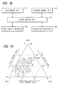
- the elution curves are arranged in parallel each other, but in the case of B 2 O 3 elution curves for SiO 2 -B 2 O 3 -Na 2 O glass, the elution curves are disordered (Fig. 19).
- the disorder is presumably attributed to the property of phase separation of Na 2 O-containing glass, that is, the disposition of the phase to separate to two different glass phases with different compositions.
- crystobalite crystal of Na 2 O glass when heat-treated is larger than that of K 2 O glass, that is two times that of K 2 O glass, but the crystallization is not so serious as to prevent the practical use. Accordingly, both Na 2 O glass and K 2 O glass have advantages K 2 O glass of reduced phase separation and crystobalite crystallization is used for the present invention.
- Glass which contains Al 2 O 3 in addition to SiO 2 , B 2 O 3 , and R 2 O is examined.
- a mixed powder of silicic acid anhydride, boric acid, and potassium carbonate prepared as to contain 86.6 % by weight of SiO 2 , 9.3 % by weight of B 2 O 3 , and 4.1 % by weight of K 2 O (approximately similar to the eighth composition) was used.
- Alumina (Al 2 O 3 ) powder was added to the mixed powder additionally in various amounts so as to prepare compositions listed in Table 2, the powder was mixed in a ball mill to obtain mixed powders having compositions of the twelfth composition to sixteenth composition listed in Table 2.
- sample glasses were prepared in the same manner as described in Example 1, and the properties of these samples were evaluated.
- the ratio (molar ratio) of Al 2 O 3 to R 2 O (in this example K 2 O) for each composition, heating temperature, measured values of thermal expansion coefficient, and relative dielectric constant are listed in Table 2. It is obvious from the experimental result that the increase of Al 2 O 3 content causes essentially no change in the thermal expansion coefficient and relative dielectric constant, and these measured values are included in the preferable range.
- a number in a small circle represents the glass composition number. From Fig. 4, it is obvious that the B 2 O 3 elution increases with the increasing of Al 2 O 3 content. However, the increased Al 2 O 3 content of as large as 90 % to K 2 O molar content results in the B 2 O 3 elution of only 1.6 mg/m 2 , therefore the increase of B 2 O 3 elution due to addition of Al 2 O 3 causes no problem.
- Fig. 5 The softening point of glass with compositions of the eighth, and the twelfth to the sixteenth is shown in Fig. 5.
- the content of Al 2 O 3 is normalized to the molar ratio to K 2 O content in glass composition in the same manner as described in Fig. 4.
- a number in a small circle represents the glass composition number. From Fig. 5, it is obvious that Al 2 O 3 content of exceeding 90 % to K 2 O molar content results in the softening point of as high as exceeding 1,100°C. Therefore, such high Al 2 O 3 content is not preferable.
- Crystobalite crystal has a transition point at about 230°C at which the crystal phase transition occurs accompanying drastic volume change, the volume change causes cracking of substrate, therefore the crystallization is not preferable.
- filler material exhibits the effect of preventing the crystallization of crystobalite crystal in borosilicate glass during the reaction between glass and filler expected when sintering, actually the crystobalite crystal may not crystallize from glass-filler composite even when the glass-filler composite is subjected to the condition which will cause the crystallization of crystobalite crystal from glass composition without filler.
- the glass with a composition which causes the crystallization of crystobalite crystal from the glass containing no filler is also suitable for the present invention if the composite comprising the glass and filler causes no crystallization of crystobalite crystal.
- Glasses with the eighth composition and the twelfth composition have such an advantage.
- a glass which causes no crystallization of crystobalite crystal using the glass solely without filler when heat-treated is advantageously used because it allows the wider selection of fillers and stabilizes the manufacturing process.
- glass contains preferably Al 2 O 3 in a molar ratio of 90 % or less to R 2 O. It is obvious that the addition of Al 2 O 3 in a molar ratio of 50 % or more to R 2 O suppresses significantly the crystallization of crystobalite crystal and 80 % or more suppresses completely the crystallization preferably.
- glasses with the seventeenth composition to twenty-third composition have reduced B 2 O 3 elution, thermal expansion coefficient, and relative dielectric constant.
- the softening point for all compositions ranges preferably from 900 to 1,060°C. No or slight crystobalite crystallization was observed for all compositions.
- ZnO powder was added in various amounts to mixed powder material of the second composition (composition is listed in Table 1) to prepare glasses, and the B 2 O 3 elution was measured in the same manner as described in Example 1.
- the relationship between ZnO content and B 2 O 3 elution is shown in Fig. 9. It is obvious in Fig. 9 that the addition of ZnO reduces dramatically the B 2 O 3 elution. It is understandable from the experimental result that the addition of ZnO is preferable for preparation of glass.
- SiO 2 -B 2 O 3 -Na 2 O-K 2 O-Al 2 O 3 -ZnO glass is featured by low B 2 O 3 elution and low relative dielectric constant.
- Glass powder of the fourteenth composition for Examples 5 to 12 and Comparative Example 1, glass powder of the ninth composition (listed in Table 1) for Examples 13 to 15, glass powder of the nineteenth composition (listed in Table 3) for Example 16, glass powder of the twenty-third composition (listed in Table 3) for Examples 17 to 20, and glass powder of the first composition (listed in Table 1) for Example 21 were prepared.
- Filler powder was mixed in various amounts in the glass powders to obtain 18 ceramic composites listed in Table 4. The average particle size (diameter) of the glass powders was about 4 microns and the average particle size of the filler was about 3 microns.
- Mullite (3Al 2 O 3 ⁇ 2SiO 2 ) was used as filler for Examples 1 to 11, 13 to 15, 17 and 18, and Comparative Example 1, mullite and alumina (Al 2 O 3 ) were used for Example 12, alumina and cordierite (2MgO-2Al 2 O 3 ⁇ 5SiO 2 ) were used for Example 16, alumina was used for Examples 19 and 21, and alumina and quartz glass (SiO 2 glass) were used for Example 20.
- green sheet with a thickness of 0.2 mm and width of 450 mm was prepared by doctor blade method.
- the green sheet was cut to 150 mm square and 50 mm square pieces.
- holes (via hole) with a diameter of 0.1 mm were punched with a 0.4 mm pitch.
- the holes were filled with copper paste by printing method, and copper paste was printed on the surface of green sheet to form a wiring pattern with a width of 0.08 mm by conventional method, then 4 to 50 green sheets were laminated by pressing at 130°C for 10 min under a pressure of 20 MPa to form green sheet laminate.
- 4 to 50 green sheets of 50 mm square were laminated by pressing at 130 °C for 10 min under a pressure of 20 MPa to form green sheet laminate without punching and printing, the laminate was used as samples for measurement of strength, relative dielectric constant, and residual carbon.
- Obtained green sheet laminate was placed in an electric furnace, atmosphere in which furnace is controllable, in an atmosphere of steam-nitrogen-hydrogen gas, the furnace temperature was raised from a room temperature to 700 to 880°C at a heating rate of Borosilicate glass-filler compositions and properties (Table 4) Glass composition number Glass content (vol %) Filler composition (vol %) Sintering temp.
- Example 5 14 90 10 0 0 0 975 2.9 200 5.0
- Example 6 14 85 15 0 0 0 975 2.9 200 5.1
- Example 7 14 80 20 0 0 0 1000 3.0 200 5.2
- Example 8 14 75 25 0 0 0 1000 3.0 210 5.2
- Example 9 14 70 30 0 0 0 1020 3.1 220 5.3
- Example 10 14 65 35 0 0 0 1025 3.1 210 5.4
- Example 11 14 60 40 0 0 0 1050 3.2 200 5.5
- Example 1 14 55 45 0 0 0 1100 3.2 200 5.5
- Example 12 14 70 22 8 0 0 1020 3.6 210 5.4
- Example 13 9 80 20 0 0 0 900 3.0 200 5.3
- Example 15 60 40 0 0 0 1000 3.2 210
- the furnace temperature was raised to the sintering temperature listed in Table 4 at a heating rate of 100°C/hr, and maintained at the sintering temperature for 2 hr to complete compact sintering, and sintered sample was obtained.
- the thermal expansion coefficient and relative dielectric constant of obtained sintered ceramics were measured in the same manner as described in Example 1.
- the bending strength of sintered samples was measured according to JIS standard (R1601), that is, the sintered ceramics was cut to specimens with a length of 38 mm, width of 4 mm, and thickness of 3 mm, and the three point bending test was carried out with a span of 30 mm.
- the measurement result is listed in Table 4.
- the thermal expansion coefficient of sintered ceramic samples of Examples 5 to 21 and Comparative Example 1 ranges from 2.0 to 3.6 ⁇ 10 -6 /°C, these values are comparable with thermal expansion coefficient of silicon (3.0 ⁇ 10 -6 /°C).
- the bending strength of sintered ceramics of Examples 5 to 21 and Comparative Example 1 is 150 MPa or higher, this value is enough for practical use.
- the sintering temperature for Examples 5 to 21 is 1,050°C or lower.
- the sintering temperature for Comparative Example 1 is 1,100°C to give unpreferable result.
- the excessive content of filler causes presumably the difficulty in sintering. Therefore, the filler content of not more than 40 % is preferable.
- the peripheral portion of sintered laminate was cut off to obtain central portion, and carbon content of the central portion was determined, and it was found that residual carbon was 200 ppm or less for Examples 5 to 21 and Comparative Example 1, the result is preferable.
- the resistance of copper conductor of sintered laminate comprising 150 mm square green sheets was measured by the four terminal method, and it was found that the specific resistance of copper conductor was as low as 3 ⁇ cm for Examples 5 to 21 and Comparative Example 1, these values are preferable.
- Heat treatment temperature for binder removal is examined. Using green sheet of Example 9, the green sheet was maintained at various temperatures to remove binder, and the time required for reducing residual carbon in sintered ceramics to 200 ppm (binder removing time) was measured. The result is shown in Fig. 10. It is obvious from Fig. 10 that the higher heat treatment temperature shorten the retention time at the temperature, and it is preferable.
- the filler content required for binder removal is examined. Green sheets which were prepared using glasses with various compositions and filler in various amounts (mullite (3Al 2 O 3 ⁇ 2SiO 2 )) were subjected to binder removal at 800 or 850°C, in some cases residual carbon content was reduced to 200 ppm or less and in some cases residual carbon content was not reduced to 200 ppm or less. For the former cases, the relationship between softening point of glass and filler content were obtained. The result is shown in Fig. 11.
- filler content required for binder removal increases with lowering of softening point of glass.
- the higher heat treatment temperature for binder removal requires the more amount of filler, because for completion of binder removal it is required that sintering of glass does not proceed during the heat treatment for binder removal. Therefore, the lower softening point and higher binder removing temperature require the higher content of filler which obstructs sintering.
- sintering compaction curves shown in Fig. 13.
- the sintering compaction curves were obtained by the following method. A green sheet laminate was placed in a transparent quartz glass reaction tube, the temperature was raised at a heating rate of 100°C/min, the shape and size of the green sheet laminate was measured by photographing the green sheet laminate at various temperatures, and the relative density was calculated from the measured values.
- a curve 131 is the sintering curve for green sheet prepared using the glass of the fourteenth composition (no filler)
- curves 132 to 138 are the sintering curves for green sheets of Examples 5 to 11.
- the curve 131 shows that a green sheet containing no filler is sintered abruptly at a temperature near 800°C and compacted.
- the curves 132 to 138 show the sintering behavior of green sheets of Examples 5 to 11 comprising glass of the fourteenth composition and 10 to 40 % by volume of filler, that is, the slope of the sintering compaction curve becomes gentle with the increasing of filler content, the gentle slope suggests difficulty in sintering.
- Sintering compaction curves shown in Fig. 13 are obtained at the retention time of zero at each temperature, and by prolonging the retention time the compaction will presumably proceed additionally.
- the sintering temperature will be unpreferably 1,050°C or higher. Therefore, when a glass with the fourteenth composition is used, the highest filler content is estimated to be 40 % by volume to allow compact sintering at temperature of 1,050°C or lower.
- Sintering compaction curve for other glasses with different compositions is obtained by parallel displacement in the abscissa direction of sintering compaction curve (curve 131) for a glass with the fourteenth composition in Fig. 13 depending on the glass softening point.
- bending strength of practical level is preferably obtained (in this case bending strength of 150 MPa or higher).
- the bending strength of 200 MPa or higher is more preferable.
- a multilayer circuit substrate (40 layers) shown in Fig. 15 was manufactured in the same manner as described in Example 5.
- the multilayer circuit substrate 17 in this example comprises via holes 9 with copper conductor, circuit 10, and a sintered glass ceramics 8.
- LSIs large-scale integrated circuit
- this instruction processor 185 an electronic computer having a main memory unit 181, an expanded memory unit 182, a system controller 183, input/output processor 184, and the instruction processor 185 was fabricated, and the processing speed of this computer was compared with that of a conventional electronic computer having an instruction processor which utilizes multilayer circuit substrate comprising mullite as substrate material and tungsten as conducting material, the processing speed of the electronic computer of the invention was twice that of the conventional electronic computer.
- Circuit substrate manufactured in the same manner as described in Example 22 is widely applied to electronic circuit devices such as electronic computers, especially when high speed and high density are required.
- the present invention provides a circuit substrate having various advantages, such as easy binder removal, easy compact sintering, thermal expansion coefficient adjustable to the thermal expansion coefficient of silicon which is preferable performance as substrate, sufficient bending strength, and sufficiently low relative dielectric constant.
- composition of the present invention has softening point of as high as 850 to 1,100°C, therefore sintering compaction scarcely occurs during heat treatment for binder removal, binder is removed with only low filler content, and compact sintering is completed within a short time.
- Glass contained in ceramic composition and the composition of the present invention has excellent water resistance, boric acid crystal does not crystallize on green sheet, and when ceramic composition of the present invention is heat-treated, crystobalite crystal does not crystallize preferably from borosilicate glass. Accordingly, the productivity of circuit substrate production is significantly enhanced by applying the present invention.
Landscapes
- Chemical & Material Sciences (AREA)
- Engineering & Computer Science (AREA)
- Life Sciences & Earth Sciences (AREA)
- Chemical Kinetics & Catalysis (AREA)
- General Chemical & Material Sciences (AREA)
- Geochemistry & Mineralogy (AREA)
- Materials Engineering (AREA)
- Organic Chemistry (AREA)
- Ceramic Engineering (AREA)
- Physics & Mathematics (AREA)
- Condensed Matter Physics & Semiconductors (AREA)
- General Physics & Mathematics (AREA)
- Computer Hardware Design (AREA)
- Microelectronics & Electronic Packaging (AREA)
- Power Engineering (AREA)
- Manufacturing & Machinery (AREA)
- Dispersion Chemistry (AREA)
- Glass Compositions (AREA)
- Compositions Of Oxide Ceramics (AREA)
Claims (9)
- Substrat de circuit multicouche avec un câblage de cuivre formé sur les couches de substrat,
dans lequelles couches de substrat sont constituées de 60 à 95 % en volume de verre amorphe ayant un point de ramollissement dans la plage de 850 à 1100°C et 5 à 40 % en volume de charge, etle verre amorphe a une composition incluant 84,0 % en poids de dioxyde de silicium (SiO2), 9,0 % en poids d'oxyde de bore (B2O3), 4,0 % en poids d'oxyde de potassium (K2O), et 3,0 % en poids d'alumine (Al2O3). - Substrat de circuit multicouche selon la revendication 1, caractérisé en ce que ledit verre amorphe a un point de ramollissement dans la plage de 900 à 1100°C.
- Substrat de circuit multicouche selon la revendication 1 ou 2, caractérisé en ce que lesdites couches de substrat ont une constante diélectrique relative de 4,3 à 5,6.
- Substrat de circuit multicouche selon l'une quelconque des revendications 1 à 3, caractérisé en ce que lesdites couches de substrat ont des trous traversants connectés au câblage.
- Substrat de circuit multicouche selon l'une quelconque des revendications 1 à 4, caractérisé en ce que lesdites couches de substrat ont un coefficient de dilatation thermique de 2,5 × 10⁻⁶ à 3,5 × 10⁻⁶/°C.
- Substrat de circuit multicouche selon la revendication 1, caractérisé en ce que ladite charge inclut au moins de la mullite.
- Module de circuit électronique utilisant un circuit multicouche selon l'une quelconque des revendications 1 à 5 et 6,
caractérisé en ce quedes circuits LSI et des broches d'entrée/sortie (E/S) sont montés sur le substrat de circuit multicouche et connectés au câblage de cuivre. - Module de circuit électronique pour un processeur d'instructions utilisant un substrat de circuit multicouche selon l'une quelconque des revendications 1 à 4,
caractérisé en ce quedes circuits LSI sont montés sur le substrat de circuit multicouche, etdes broches E/S et des parties de refroidissement sont connectées au substrat de circuit multicouche. - Ordinateur électronique comportant :un module de circuit électronique pour un processeur d'instructions utilisant un substrat de circuit multicouche selon l'une quelconque des revendications 1 à 5 et 6,caractérisé en ce quedes circuits LSI sont montés sur le substrat de circuit multicouche, et des broches E/S et des parties de refroidissement sont connectées au substrat de circuit multicouche,un contrôleur système est connecté audit module de circuit électronique,une mémoire est connectée audit contrôleur système, etun processeur E/S est connecté audit contrôleur système.
Applications Claiming Priority (3)
| Application Number | Priority Date | Filing Date | Title |
|---|---|---|---|
| JP19580694 | 1994-08-19 | ||
| JP19580694 | 1994-08-19 | ||
| EP95111855A EP0697725B1 (fr) | 1994-08-19 | 1995-07-27 | Composition céramique pour substrat de circuit et méthode de fabrication |
Related Parent Applications (1)
| Application Number | Title | Priority Date | Filing Date |
|---|---|---|---|
| EP95111855A Division EP0697725B1 (fr) | 1994-08-19 | 1995-07-27 | Composition céramique pour substrat de circuit et méthode de fabrication |
Publications (3)
| Publication Number | Publication Date |
|---|---|
| EP1083600A2 EP1083600A2 (fr) | 2001-03-14 |
| EP1083600A3 EP1083600A3 (fr) | 2005-05-25 |
| EP1083600B1 true EP1083600B1 (fr) | 2007-02-14 |
Family
ID=16347298
Family Applications (2)
| Application Number | Title | Priority Date | Filing Date |
|---|---|---|---|
| EP00124369A Expired - Lifetime EP1083600B1 (fr) | 1994-08-19 | 1995-07-27 | Substrat de circuit multi-couche |
| EP95111855A Expired - Lifetime EP0697725B1 (fr) | 1994-08-19 | 1995-07-27 | Composition céramique pour substrat de circuit et méthode de fabrication |
Family Applications After (1)
| Application Number | Title | Priority Date | Filing Date |
|---|---|---|---|
| EP95111855A Expired - Lifetime EP0697725B1 (fr) | 1994-08-19 | 1995-07-27 | Composition céramique pour substrat de circuit et méthode de fabrication |
Country Status (3)
| Country | Link |
|---|---|
| US (2) | US5825632A (fr) |
| EP (2) | EP1083600B1 (fr) |
| DE (2) | DE69528868T2 (fr) |
Families Citing this family (26)
| Publication number | Priority date | Publication date | Assignee | Title |
|---|---|---|---|---|
| EP1083600B1 (fr) * | 1994-08-19 | 2007-02-14 | Hitachi, Ltd. | Substrat de circuit multi-couche |
| JP3860336B2 (ja) * | 1998-04-28 | 2006-12-20 | 日本特殊陶業株式会社 | ガラスセラミック複合体 |
| US6288344B1 (en) * | 1999-08-20 | 2001-09-11 | Cardiac Pacemakers, Inc. | Integrated EMI shield utilizing a hybrid edge |
| US6444921B1 (en) * | 2000-02-03 | 2002-09-03 | Fujitsu Limited | Reduced stress and zero stress interposers for integrated-circuit chips, multichip substrates, and the like |
| JP2001244376A (ja) * | 2000-02-28 | 2001-09-07 | Hitachi Ltd | 半導体装置 |
| JP3531573B2 (ja) * | 2000-03-17 | 2004-05-31 | 株式会社村田製作所 | 積層型セラミック電子部品およびその製造方法ならびに電子装置 |
| JP2001332859A (ja) * | 2000-05-22 | 2001-11-30 | Murata Mfg Co Ltd | 積層型セラミック電子部品およびその製造方法ならびに電子装置 |
| JP3407716B2 (ja) | 2000-06-08 | 2003-05-19 | 株式会社村田製作所 | 複合積層電子部品 |
| EP1323682A3 (fr) * | 2001-12-25 | 2004-01-21 | Ngk Spark Plug Co., Ltd | Matériau diélectrique et corps fritté diélectrique, et carte à circuit |
| DE10215654A1 (de) * | 2002-04-09 | 2003-11-06 | Infineon Technologies Ag | Elektronisches Bauteil mit mindestens einem Halbleiterchip und Flip-Chip-Kontakten sowie Verfahren zu seiner Herstellung |
| KR20030074582A (ko) * | 2003-09-03 | 2003-09-19 | 학교법인 한국정보통신학원 | 초고주파 다층회로 구조 및 제작 방법 |
| US7919804B2 (en) * | 2005-11-08 | 2011-04-05 | Oracle America, Inc. | Power distribution for high-speed integrated circuits |
| US9233253B2 (en) | 2012-01-16 | 2016-01-12 | Greatbatch Ltd. | EMI filtered co-connected hermetic feedthrough, feedthrough capacitor and leadwire assembly for an active implantable medical device |
| US8193456B2 (en) * | 2008-06-30 | 2012-06-05 | Ngk Spark Plug Co., Ltd. | Electrical inspection substrate unit and manufacturing method therefore |
| US11198014B2 (en) | 2011-03-01 | 2021-12-14 | Greatbatch Ltd. | Hermetically sealed filtered feedthrough assembly having a capacitor with an oxide resistant electrical connection to an active implantable medical device housing |
| US10596369B2 (en) | 2011-03-01 | 2020-03-24 | Greatbatch Ltd. | Low equivalent series resistance RF filter for an active implantable medical device |
| US10420949B2 (en) | 2012-01-16 | 2019-09-24 | Greatbatch Ltd. | Method of manufacturing a feedthrough insulator for an active implantable medical device incorporating a post conductive paste filled pressing step |
| US9889306B2 (en) | 2012-01-16 | 2018-02-13 | Greatbatch Ltd. | Hermetically sealed feedthrough with co-fired filled via and conductive insert for an active implantable medical device |
| US10046166B2 (en) | 2012-01-16 | 2018-08-14 | Greatbatch Ltd. | EMI filtered co-connected hermetic feedthrough, feedthrough capacitor and leadwire assembly for an active implantable medical device |
| US10881867B2 (en) | 2012-01-16 | 2021-01-05 | Greatbatch Ltd. | Method for providing a hermetically sealed feedthrough with co-fired filled via for an active implantable medical device |
| US20130229777A1 (en) * | 2012-03-01 | 2013-09-05 | Infineon Technologies Ag | Chip arrangements and methods for forming a chip arrangement |
| USRE46699E1 (en) | 2013-01-16 | 2018-02-06 | Greatbatch Ltd. | Low impedance oxide resistant grounded capacitor for an AIMD |
| CN109644556B (zh) | 2016-11-02 | 2021-09-03 | 株式会社村田制作所 | 陶瓷电子部件以及陶瓷电子部件的制造方法 |
| US10249415B2 (en) | 2017-01-06 | 2019-04-02 | Greatbatch Ltd. | Process for manufacturing a leadless feedthrough for an active implantable medical device |
| JP2019060817A (ja) * | 2017-09-28 | 2019-04-18 | 日本特殊陶業株式会社 | 電子部品検査装置用配線基板 |
| CN115866936B (zh) * | 2023-03-01 | 2023-05-30 | 四川斯艾普电子科技有限公司 | 一种采用厚薄膜工艺实现多层电路板的方法 |
Family Cites Families (22)
| Publication number | Priority date | Publication date | Assignee | Title |
|---|---|---|---|---|
| US34887A (en) * | 1862-04-08 | Improvement in fish-traps | ||
| US2247331A (en) * | 1938-01-22 | 1941-06-24 | Ferguson John | Glassmaking batch |
| JPS591224B2 (ja) * | 1978-09-06 | 1984-01-11 | 東芝セラミツクス株式会社 | ランプフィラメント保持部材用硼珪酸ガラス焼結体 |
| JPS6028296A (ja) * | 1983-07-27 | 1985-02-13 | 株式会社日立製作所 | セラミツク多層配線回路板 |
| JPS60235744A (ja) * | 1984-05-04 | 1985-11-22 | Asahi Glass Co Ltd | セラミック基板用組成物 |
| JPS62287658A (ja) * | 1986-06-06 | 1987-12-14 | Hitachi Ltd | セラミックス多層回路板 |
| US4897509A (en) * | 1987-04-27 | 1990-01-30 | Corning Incorporated | Glass-ceramics for electronic packaging |
| US4788165A (en) * | 1987-10-07 | 1988-11-29 | Corning Glass Works | Copper-exuding, boroaluminosilicate glasses |
| JPH0650792B2 (ja) * | 1987-10-19 | 1994-06-29 | インターナシヨナル・ビジネス・マシーンズ・コーポレーシヨン | 耐酸化金属導体を含むセラミック構造体及びその製造方法 |
| JPH01145349A (ja) * | 1987-11-30 | 1989-06-07 | Agency Of Ind Science & Technol | 多孔質ガラス用組成物 |
| JPH0249550A (ja) | 1988-08-11 | 1990-02-19 | Suzuki Seifunshiyo:Kk | そば粥の製造方法 |
| EP0360971A3 (fr) * | 1988-08-31 | 1991-07-17 | Mitsui Mining & Smelting Co., Ltd. | Substrat de montage et sa méthode de production et circuit imprimé ayant une fonction de connecteur et sa méthode de connexion |
| US4942076A (en) * | 1988-11-03 | 1990-07-17 | Micro Substrates, Inc. | Ceramic substrate with metal filled via holes for hybrid microcircuits and method of making the same |
| JPH03252353A (ja) * | 1990-02-28 | 1991-11-11 | Nec Corp | 低温焼結性低誘電率無機組成物 |
| US5256470A (en) * | 1990-10-11 | 1993-10-26 | Aluminum Company Of America | Crystal growth inhibitor for glassy low dielectric inorganic composition |
| JP2551224B2 (ja) * | 1990-10-17 | 1996-11-06 | 日本電気株式会社 | 多層配線基板および多層配線基板の製造方法 |
| JPH05116985A (ja) * | 1991-05-22 | 1993-05-14 | Ngk Spark Plug Co Ltd | セラミツク基板 |
| JPH07108832B2 (ja) * | 1991-09-26 | 1995-11-22 | インターナシヨナル・ビジネス・マシーンズ・コーポレーシヨン | 低誘電率基板およびその製法 |
| JPH05254923A (ja) * | 1992-03-10 | 1993-10-05 | Hitachi Ltd | セラミック組成物及びセラミック回路基板 |
| US5407473A (en) * | 1993-12-29 | 1995-04-18 | Matsushita Electric Industrial Co., Ltd. | Conductive ink |
| EP1083600B1 (fr) * | 1994-08-19 | 2007-02-14 | Hitachi, Ltd. | Substrat de circuit multi-couche |
| US5805425A (en) * | 1996-09-24 | 1998-09-08 | Texas Instruments Incorporated | Microelectronic assemblies including Z-axis conductive films |
-
1995
- 1995-07-27 EP EP00124369A patent/EP1083600B1/fr not_active Expired - Lifetime
- 1995-07-27 DE DE69528868T patent/DE69528868T2/de not_active Expired - Fee Related
- 1995-07-27 DE DE69535391T patent/DE69535391T2/de not_active Expired - Fee Related
- 1995-07-27 EP EP95111855A patent/EP0697725B1/fr not_active Expired - Lifetime
- 1995-08-08 US US08/512,705 patent/US5825632A/en not_active Expired - Fee Related
-
1998
- 1998-06-24 US US09/103,812 patent/US6118671A/en not_active Expired - Fee Related
Also Published As
| Publication number | Publication date |
|---|---|
| EP0697725A3 (fr) | 1997-02-19 |
| DE69535391T2 (de) | 2007-10-31 |
| DE69535391D1 (de) | 2007-03-29 |
| EP0697725B1 (fr) | 2002-11-20 |
| US5825632A (en) | 1998-10-20 |
| US6118671A (en) | 2000-09-12 |
| DE69528868T2 (de) | 2003-03-27 |
| EP1083600A3 (fr) | 2005-05-25 |
| EP0697725A2 (fr) | 1996-02-21 |
| EP1083600A2 (fr) | 2001-03-14 |
| DE69528868D1 (de) | 2003-01-02 |
Similar Documents
| Publication | Publication Date | Title |
|---|---|---|
| EP1083600B1 (fr) | Substrat de circuit multi-couche | |
| EP0163155B1 (fr) | Céramiques cuites à basse température | |
| EP0163548B1 (fr) | Procédé pour produire des plaquettes céramiques multicouches pour circuits | |
| US5258335A (en) | Low dielectric, low temperature fired glass ceramics | |
| JPH04243962A (ja) | 多層セラミックパッケージ用低誘電性無機組成物、及びその調製方法 | |
| EP0552522B1 (fr) | Vitrocéramiques à constante diélectrique faible, frittées à des basses températures | |
| EP0478971A2 (fr) | Composition diélectrique contenant de la cordiérite et du verre | |
| EP0196670B1 (fr) | Supports céramiques pour circuits microélectroniques et procédé de leur fabrication | |
| EP0532842A1 (fr) | Composition inorganique faiblement diélectrique pour un assemblage céramique multicouche | |
| JPH08333157A (ja) | 配線基板、その製造方法、非晶質ガラス、配線基板用セラミック組成物、電子回路装置、電子計算機用モジュール、および電子計算機 | |
| EP0280819A2 (fr) | Résistances électriques, pâte pour résistances électriques et méthode de fabrication | |
| JP4569000B2 (ja) | 高周波用低温焼結誘電体材料およびその焼結体 | |
| US5118643A (en) | Low dielectric inorganic composition for multilayer ceramic package containing titanium silicate glass | |
| JPH0617250B2 (ja) | ガラスセラミツク焼結体 | |
| JP3690312B2 (ja) | 電子回路装置及び電子計算機用モジュール | |
| JP2699919B2 (ja) | 多層配線基板とその製造方法、及びそれに用いるシリカ焼結体の製造方法 | |
| JP2002047058A (ja) | 配線基板用セラミック組成物 | |
| JP3125500B2 (ja) | セラミックス基板 | |
| JP2002047029A (ja) | 非晶質ガラス | |
| US5226959A (en) | Gallium-containing glassy low dielectric ceramic compositions | |
| JPH0226864A (ja) | 低温焼成セラミックス組成物 | |
| JP2723710B2 (ja) | 多層ガラスセラミック基板及びその製造方法 | |
| JP2002060267A (ja) | 配線基板の製造方法 | |
| JPH05238813A (ja) | 低誘電率、低温焼成ガラスセラミック | |
| JPH06112604A (ja) | 多層ガラスセラミック基板とその製造方法 |
Legal Events
| Date | Code | Title | Description |
|---|---|---|---|
| PUAI | Public reference made under article 153(3) epc to a published international application that has entered the european phase |
Free format text: ORIGINAL CODE: 0009012 |
|
| AC | Divisional application: reference to earlier application |
Ref document number: 697725 Country of ref document: EP |
|
| AK | Designated contracting states |
Kind code of ref document: A2 Designated state(s): DE FR |
|
| RIN1 | Information on inventor provided before grant (corrected) |
Inventor name: NAKAMURA, MASATO Inventor name: OKAMOTO, MASAHIDE Inventor name: IWANAGA, SHOICHI Inventor name: TAGAMI, FUMIKAZU Inventor name: ISHIHARA, SHOUSAKU Inventor name: MORITA, KOUSAKU Inventor name: TANEI, HIRAYOSHI Inventor name: KOBAYASHI, FUMIYUKI |
|
| PUAL | Search report despatched |
Free format text: ORIGINAL CODE: 0009013 |
|
| AK | Designated contracting states |
Kind code of ref document: A3 Designated state(s): DE FR |
|
| 17P | Request for examination filed |
Effective date: 20051010 |
|
| AKX | Designation fees paid |
Designated state(s): DE FR |
|
| GRAP | Despatch of communication of intention to grant a patent |
Free format text: ORIGINAL CODE: EPIDOSNIGR1 |
|
| GRAS | Grant fee paid |
Free format text: ORIGINAL CODE: EPIDOSNIGR3 |
|
| GRAA | (expected) grant |
Free format text: ORIGINAL CODE: 0009210 |
|
| AC | Divisional application: reference to earlier application |
Ref document number: 0697725 Country of ref document: EP Kind code of ref document: P |
|
| AK | Designated contracting states |
Kind code of ref document: B1 Designated state(s): DE FR |
|
| REF | Corresponds to: |
Ref document number: 69535391 Country of ref document: DE Date of ref document: 20070329 Kind code of ref document: P |
|
| ET | Fr: translation filed | ||
| PLBE | No opposition filed within time limit |
Free format text: ORIGINAL CODE: 0009261 |
|
| STAA | Information on the status of an ep patent application or granted ep patent |
Free format text: STATUS: NO OPPOSITION FILED WITHIN TIME LIMIT |
|
| 26N | No opposition filed |
Effective date: 20071115 |
|
| PGFP | Annual fee paid to national office [announced via postgrant information from national office to epo] |
Ref country code: DE Payment date: 20080908 Year of fee payment: 14 |
|
| PGFP | Annual fee paid to national office [announced via postgrant information from national office to epo] |
Ref country code: FR Payment date: 20080623 Year of fee payment: 14 |
|
| REG | Reference to a national code |
Ref country code: FR Ref legal event code: ST Effective date: 20100331 |
|
| PG25 | Lapsed in a contracting state [announced via postgrant information from national office to epo] |
Ref country code: FR Free format text: LAPSE BECAUSE OF NON-PAYMENT OF DUE FEES Effective date: 20090731 |
|
| PG25 | Lapsed in a contracting state [announced via postgrant information from national office to epo] |
Ref country code: DE Free format text: LAPSE BECAUSE OF NON-PAYMENT OF DUE FEES Effective date: 20100202 |