EP1077486B1 - Semiconductor device - Google Patents
Semiconductor device Download PDFInfo
- Publication number
- EP1077486B1 EP1077486B1 EP99918319A EP99918319A EP1077486B1 EP 1077486 B1 EP1077486 B1 EP 1077486B1 EP 99918319 A EP99918319 A EP 99918319A EP 99918319 A EP99918319 A EP 99918319A EP 1077486 B1 EP1077486 B1 EP 1077486B1
- Authority
- EP
- European Patent Office
- Prior art keywords
- film
- layer
- semiconductor device
- gas
- insulating film
- Prior art date
- Legal status (The legal status is an assumption and is not a legal conclusion. Google has not performed a legal analysis and makes no representation as to the accuracy of the status listed.)
- Expired - Lifetime
Links
- 239000004065 semiconductor Substances 0.000 title claims description 57
- 239000000758 substrate Substances 0.000 claims abstract description 22
- 229910052799 carbon Inorganic materials 0.000 claims abstract description 11
- OKTJSMMVPCPJKN-UHFFFAOYSA-N Carbon Chemical compound [C] OKTJSMMVPCPJKN-UHFFFAOYSA-N 0.000 claims abstract description 8
- 239000010949 copper Substances 0.000 claims description 91
- 239000010936 titanium Substances 0.000 claims description 44
- 229910052751 metal Inorganic materials 0.000 claims description 13
- 239000002184 metal Substances 0.000 claims description 13
- 229910052802 copper Inorganic materials 0.000 claims description 11
- 229910052719 titanium Inorganic materials 0.000 claims description 10
- 229910052760 oxygen Inorganic materials 0.000 claims description 8
- IJGRMHOSHXDMSA-UHFFFAOYSA-N Atomic nitrogen Chemical compound N#N IJGRMHOSHXDMSA-UHFFFAOYSA-N 0.000 claims description 7
- RYGMFSIKBFXOCR-UHFFFAOYSA-N Copper Chemical compound [Cu] RYGMFSIKBFXOCR-UHFFFAOYSA-N 0.000 claims description 6
- QVGXLLKOCUKJST-UHFFFAOYSA-N atomic oxygen Chemical compound [O] QVGXLLKOCUKJST-UHFFFAOYSA-N 0.000 claims description 5
- 239000010955 niobium Substances 0.000 claims description 5
- 239000001301 oxygen Substances 0.000 claims description 5
- RTAQQCXQSZGOHL-UHFFFAOYSA-N Titanium Chemical compound [Ti] RTAQQCXQSZGOHL-UHFFFAOYSA-N 0.000 claims description 4
- 229910052796 boron Inorganic materials 0.000 claims description 4
- 239000011651 chromium Substances 0.000 claims description 4
- 229910052750 molybdenum Inorganic materials 0.000 claims description 4
- 229910052715 tantalum Inorganic materials 0.000 claims description 4
- ZOXJGFHDIHLPTG-UHFFFAOYSA-N Boron Chemical compound [B] ZOXJGFHDIHLPTG-UHFFFAOYSA-N 0.000 claims description 3
- 229910052804 chromium Inorganic materials 0.000 claims description 3
- 150000001875 compounds Chemical class 0.000 claims description 3
- 229910052758 niobium Inorganic materials 0.000 claims description 3
- 229910052757 nitrogen Inorganic materials 0.000 claims description 3
- 229910052726 zirconium Inorganic materials 0.000 claims description 3
- VYZAMTAEIAYCRO-UHFFFAOYSA-N Chromium Chemical compound [Cr] VYZAMTAEIAYCRO-UHFFFAOYSA-N 0.000 claims description 2
- ZOKXTWBITQBERF-UHFFFAOYSA-N Molybdenum Chemical compound [Mo] ZOKXTWBITQBERF-UHFFFAOYSA-N 0.000 claims description 2
- QCWXUUIWCKQGHC-UHFFFAOYSA-N Zirconium Chemical compound [Zr] QCWXUUIWCKQGHC-UHFFFAOYSA-N 0.000 claims description 2
- 229910017052 cobalt Inorganic materials 0.000 claims description 2
- 239000010941 cobalt Substances 0.000 claims description 2
- GUTLYIVDDKVIGB-UHFFFAOYSA-N cobalt atom Chemical compound [Co] GUTLYIVDDKVIGB-UHFFFAOYSA-N 0.000 claims description 2
- 239000011733 molybdenum Substances 0.000 claims description 2
- GUCVJGMIXFAOAE-UHFFFAOYSA-N niobium atom Chemical compound [Nb] GUCVJGMIXFAOAE-UHFFFAOYSA-N 0.000 claims description 2
- GUVRBAGPIYLISA-UHFFFAOYSA-N tantalum atom Chemical compound [Ta] GUVRBAGPIYLISA-UHFFFAOYSA-N 0.000 claims description 2
- 229910052731 fluorine Inorganic materials 0.000 abstract description 5
- 239000011737 fluorine Substances 0.000 abstract description 3
- YCKRFDGAMUMZLT-UHFFFAOYSA-N Fluorine atom Chemical compound [F] YCKRFDGAMUMZLT-UHFFFAOYSA-N 0.000 abstract 1
- 239000010408 film Substances 0.000 description 238
- 239000010410 layer Substances 0.000 description 127
- 239000007789 gas Substances 0.000 description 74
- 238000000034 method Methods 0.000 description 61
- 210000002381 plasma Anatomy 0.000 description 49
- VYPSYNLAJGMNEJ-UHFFFAOYSA-N Silicium dioxide Chemical compound O=[Si]=O VYPSYNLAJGMNEJ-UHFFFAOYSA-N 0.000 description 24
- 238000000151 deposition Methods 0.000 description 22
- 230000008021 deposition Effects 0.000 description 20
- 238000009792 diffusion process Methods 0.000 description 17
- 238000001004 secondary ion mass spectrometry Methods 0.000 description 14
- 238000004458 analytical method Methods 0.000 description 13
- 238000002474 experimental method Methods 0.000 description 13
- 239000000463 material Substances 0.000 description 13
- 229910052681 coesite Inorganic materials 0.000 description 12
- 229910052906 cristobalite Inorganic materials 0.000 description 12
- 229910052710 silicon Inorganic materials 0.000 description 12
- 239000000377 silicon dioxide Substances 0.000 description 12
- 229910052682 stishovite Inorganic materials 0.000 description 12
- 229910052905 tridymite Inorganic materials 0.000 description 12
- 230000000052 comparative effect Effects 0.000 description 10
- UMIVXZPTRXBADB-UHFFFAOYSA-N benzocyclobutene Chemical compound C1=CC=C2CCC2=C1 UMIVXZPTRXBADB-UHFFFAOYSA-N 0.000 description 9
- XUIMIQQOPSSXEZ-UHFFFAOYSA-N Silicon Chemical compound [Si] XUIMIQQOPSSXEZ-UHFFFAOYSA-N 0.000 description 8
- 230000004888 barrier function Effects 0.000 description 8
- 239000010703 silicon Substances 0.000 description 8
- 238000000427 thin-film deposition Methods 0.000 description 8
- 238000000137 annealing Methods 0.000 description 7
- 239000011229 interlayer Substances 0.000 description 7
- 230000008018 melting Effects 0.000 description 7
- 238000002844 melting Methods 0.000 description 7
- 238000004544 sputter deposition Methods 0.000 description 6
- 238000012545 processing Methods 0.000 description 5
- ATJFFYVFTNAWJD-UHFFFAOYSA-N Tin Chemical compound [Sn] ATJFFYVFTNAWJD-UHFFFAOYSA-N 0.000 description 4
- 150000002500 ions Chemical class 0.000 description 4
- 238000004519 manufacturing process Methods 0.000 description 4
- 229910001512 metal fluoride Inorganic materials 0.000 description 4
- 229910052718 tin Inorganic materials 0.000 description 4
- 229920003209 poly(hydridosilsesquioxane) Polymers 0.000 description 3
- 229920001721 polyimide Polymers 0.000 description 3
- 239000002344 surface layer Substances 0.000 description 3
- 229910052721 tungsten Inorganic materials 0.000 description 3
- XKRFYHLGVUSROY-UHFFFAOYSA-N Argon Chemical compound [Ar] XKRFYHLGVUSROY-UHFFFAOYSA-N 0.000 description 2
- PXGOKWXKJXAPGV-UHFFFAOYSA-N Fluorine Chemical compound FF PXGOKWXKJXAPGV-UHFFFAOYSA-N 0.000 description 2
- 229910020177 SiOF Inorganic materials 0.000 description 2
- 229910003074 TiCl4 Inorganic materials 0.000 description 2
- 150000001722 carbon compounds Chemical class 0.000 description 2
- 238000005229 chemical vapour deposition Methods 0.000 description 2
- 230000007423 decrease Effects 0.000 description 2
- 238000005530 etching Methods 0.000 description 2
- 150000002222 fluorine compounds Chemical class 0.000 description 2
- 239000013081 microcrystal Substances 0.000 description 2
- 238000013508 migration Methods 0.000 description 2
- 238000000859 sublimation Methods 0.000 description 2
- 230000008022 sublimation Effects 0.000 description 2
- XJDNKRIXUMDJCW-UHFFFAOYSA-J titanium tetrachloride Chemical compound Cl[Ti](Cl)(Cl)Cl XJDNKRIXUMDJCW-UHFFFAOYSA-J 0.000 description 2
- 239000004642 Polyimide Substances 0.000 description 1
- 229910007991 Si-N Inorganic materials 0.000 description 1
- 229910006294 Si—N Inorganic materials 0.000 description 1
- 229910004479 Ta2N Inorganic materials 0.000 description 1
- 229910008479 TiSi2 Inorganic materials 0.000 description 1
- 229910008599 TiW Inorganic materials 0.000 description 1
- NRTOMJZYCJJWKI-UHFFFAOYSA-N Titanium nitride Chemical compound [Ti]#N NRTOMJZYCJJWKI-UHFFFAOYSA-N 0.000 description 1
- 238000002441 X-ray diffraction Methods 0.000 description 1
- 239000012790 adhesive layer Substances 0.000 description 1
- 229910052782 aluminium Inorganic materials 0.000 description 1
- XAGFODPZIPBFFR-UHFFFAOYSA-N aluminium Chemical compound [Al] XAGFODPZIPBFFR-UHFFFAOYSA-N 0.000 description 1
- 229910052786 argon Inorganic materials 0.000 description 1
- 230000005540 biological transmission Effects 0.000 description 1
- 230000015572 biosynthetic process Effects 0.000 description 1
- DFJQEGUNXWZVAH-UHFFFAOYSA-N bis($l^{2}-silanylidene)titanium Chemical compound [Si]=[Ti]=[Si] DFJQEGUNXWZVAH-UHFFFAOYSA-N 0.000 description 1
- 230000015556 catabolic process Effects 0.000 description 1
- 238000006243 chemical reaction Methods 0.000 description 1
- KPUWHANPEXNPJT-UHFFFAOYSA-N disiloxane Chemical class [SiH3]O[SiH3] KPUWHANPEXNPJT-UHFFFAOYSA-N 0.000 description 1
- 230000001747 exhibiting effect Effects 0.000 description 1
- 238000010438 heat treatment Methods 0.000 description 1
- 230000002401 inhibitory effect Effects 0.000 description 1
- 230000010354 integration Effects 0.000 description 1
- 230000003993 interaction Effects 0.000 description 1
- 230000007257 malfunction Effects 0.000 description 1
- 150000002739 metals Chemical class 0.000 description 1
- 239000000203 mixture Substances 0.000 description 1
- 238000005498 polishing Methods 0.000 description 1
- 238000007517 polishing process Methods 0.000 description 1
- 229920000642 polymer Polymers 0.000 description 1
- 230000002265 prevention Effects 0.000 description 1
- 238000011160 research Methods 0.000 description 1
- 239000000126 substance Substances 0.000 description 1
- -1 that is Substances 0.000 description 1
- 239000010409 thin film Substances 0.000 description 1
Images


Classifications
-
- H—ELECTRICITY
- H01—ELECTRIC ELEMENTS
- H01L—SEMICONDUCTOR DEVICES NOT COVERED BY CLASS H10
- H01L21/00—Processes or apparatus adapted for the manufacture or treatment of semiconductor or solid state devices or of parts thereof
- H01L21/02—Manufacture or treatment of semiconductor devices or of parts thereof
- H01L21/02104—Forming layers
- H01L21/02107—Forming insulating materials on a substrate
- H01L21/02109—Forming insulating materials on a substrate characterised by the type of layer, e.g. type of material, porous/non-porous, pre-cursors, mixtures or laminates
- H01L21/02112—Forming insulating materials on a substrate characterised by the type of layer, e.g. type of material, porous/non-porous, pre-cursors, mixtures or laminates characterised by the material of the layer
- H01L21/02118—Forming insulating materials on a substrate characterised by the type of layer, e.g. type of material, porous/non-porous, pre-cursors, mixtures or laminates characterised by the material of the layer carbon based polymeric organic or inorganic material, e.g. polyimides, poly cyclobutene or PVC
- H01L21/0212—Forming insulating materials on a substrate characterised by the type of layer, e.g. type of material, porous/non-porous, pre-cursors, mixtures or laminates characterised by the material of the layer carbon based polymeric organic or inorganic material, e.g. polyimides, poly cyclobutene or PVC the material being fluoro carbon compounds, e.g.(CFx) n, (CHxFy) n or polytetrafluoroethylene
-
- H—ELECTRICITY
- H01—ELECTRIC ELEMENTS
- H01L—SEMICONDUCTOR DEVICES NOT COVERED BY CLASS H10
- H01L21/00—Processes or apparatus adapted for the manufacture or treatment of semiconductor or solid state devices or of parts thereof
- H01L21/70—Manufacture or treatment of devices consisting of a plurality of solid state components formed in or on a common substrate or of parts thereof; Manufacture of integrated circuit devices or of parts thereof
- H01L21/71—Manufacture of specific parts of devices defined in group H01L21/70
- H01L21/768—Applying interconnections to be used for carrying current between separate components within a device comprising conductors and dielectrics
-
- H—ELECTRICITY
- H01—ELECTRIC ELEMENTS
- H01L—SEMICONDUCTOR DEVICES NOT COVERED BY CLASS H10
- H01L21/00—Processes or apparatus adapted for the manufacture or treatment of semiconductor or solid state devices or of parts thereof
- H01L21/02—Manufacture or treatment of semiconductor devices or of parts thereof
- H01L21/02104—Forming layers
- H01L21/02107—Forming insulating materials on a substrate
- H01L21/02225—Forming insulating materials on a substrate characterised by the process for the formation of the insulating layer
- H01L21/0226—Forming insulating materials on a substrate characterised by the process for the formation of the insulating layer formation by a deposition process
- H01L21/02263—Forming insulating materials on a substrate characterised by the process for the formation of the insulating layer formation by a deposition process deposition from the gas or vapour phase
- H01L21/02271—Forming insulating materials on a substrate characterised by the process for the formation of the insulating layer formation by a deposition process deposition from the gas or vapour phase deposition by decomposition or reaction of gaseous or vapour phase compounds, i.e. chemical vapour deposition
- H01L21/02274—Forming insulating materials on a substrate characterised by the process for the formation of the insulating layer formation by a deposition process deposition from the gas or vapour phase deposition by decomposition or reaction of gaseous or vapour phase compounds, i.e. chemical vapour deposition in the presence of a plasma [PECVD]
-
- H—ELECTRICITY
- H01—ELECTRIC ELEMENTS
- H01L—SEMICONDUCTOR DEVICES NOT COVERED BY CLASS H10
- H01L21/00—Processes or apparatus adapted for the manufacture or treatment of semiconductor or solid state devices or of parts thereof
- H01L21/02—Manufacture or treatment of semiconductor devices or of parts thereof
- H01L21/04—Manufacture or treatment of semiconductor devices or of parts thereof the devices having potential barriers, e.g. a PN junction, depletion layer or carrier concentration layer
- H01L21/18—Manufacture or treatment of semiconductor devices or of parts thereof the devices having potential barriers, e.g. a PN junction, depletion layer or carrier concentration layer the devices having semiconductor bodies comprising elements of Group IV of the Periodic Table or AIIIBV compounds with or without impurities, e.g. doping materials
- H01L21/30—Treatment of semiconductor bodies using processes or apparatus not provided for in groups H01L21/20 - H01L21/26
- H01L21/31—Treatment of semiconductor bodies using processes or apparatus not provided for in groups H01L21/20 - H01L21/26 to form insulating layers thereon, e.g. for masking or by using photolithographic techniques; After treatment of these layers; Selection of materials for these layers
- H01L21/312—Organic layers, e.g. photoresist
- H01L21/3127—Layers comprising fluoro (hydro)carbon compounds, e.g. polytetrafluoroethylene
-
- H—ELECTRICITY
- H01—ELECTRIC ELEMENTS
- H01L—SEMICONDUCTOR DEVICES NOT COVERED BY CLASS H10
- H01L21/00—Processes or apparatus adapted for the manufacture or treatment of semiconductor or solid state devices or of parts thereof
- H01L21/70—Manufacture or treatment of devices consisting of a plurality of solid state components formed in or on a common substrate or of parts thereof; Manufacture of integrated circuit devices or of parts thereof
- H01L21/71—Manufacture of specific parts of devices defined in group H01L21/70
- H01L21/768—Applying interconnections to be used for carrying current between separate components within a device comprising conductors and dielectrics
- H01L21/76801—Applying interconnections to be used for carrying current between separate components within a device comprising conductors and dielectrics characterised by the formation and the after-treatment of the dielectrics, e.g. smoothing
- H01L21/76822—Modification of the material of dielectric layers, e.g. grading, after-treatment to improve the stability of the layers, to increase their density etc.
- H01L21/76826—Modification of the material of dielectric layers, e.g. grading, after-treatment to improve the stability of the layers, to increase their density etc. by contacting the layer with gases, liquids or plasmas
-
- H—ELECTRICITY
- H01—ELECTRIC ELEMENTS
- H01L—SEMICONDUCTOR DEVICES NOT COVERED BY CLASS H10
- H01L21/00—Processes or apparatus adapted for the manufacture or treatment of semiconductor or solid state devices or of parts thereof
- H01L21/70—Manufacture or treatment of devices consisting of a plurality of solid state components formed in or on a common substrate or of parts thereof; Manufacture of integrated circuit devices or of parts thereof
- H01L21/71—Manufacture of specific parts of devices defined in group H01L21/70
- H01L21/768—Applying interconnections to be used for carrying current between separate components within a device comprising conductors and dielectrics
- H01L21/76801—Applying interconnections to be used for carrying current between separate components within a device comprising conductors and dielectrics characterised by the formation and the after-treatment of the dielectrics, e.g. smoothing
- H01L21/76822—Modification of the material of dielectric layers, e.g. grading, after-treatment to improve the stability of the layers, to increase their density etc.
- H01L21/76828—Modification of the material of dielectric layers, e.g. grading, after-treatment to improve the stability of the layers, to increase their density etc. thermal treatment
-
- H—ELECTRICITY
- H01—ELECTRIC ELEMENTS
- H01L—SEMICONDUCTOR DEVICES NOT COVERED BY CLASS H10
- H01L21/00—Processes or apparatus adapted for the manufacture or treatment of semiconductor or solid state devices or of parts thereof
- H01L21/70—Manufacture or treatment of devices consisting of a plurality of solid state components formed in or on a common substrate or of parts thereof; Manufacture of integrated circuit devices or of parts thereof
- H01L21/71—Manufacture of specific parts of devices defined in group H01L21/70
- H01L21/768—Applying interconnections to be used for carrying current between separate components within a device comprising conductors and dielectrics
- H01L21/76801—Applying interconnections to be used for carrying current between separate components within a device comprising conductors and dielectrics characterised by the formation and the after-treatment of the dielectrics, e.g. smoothing
- H01L21/76829—Applying interconnections to be used for carrying current between separate components within a device comprising conductors and dielectrics characterised by the formation and the after-treatment of the dielectrics, e.g. smoothing characterised by the formation of thin functional dielectric layers, e.g. dielectric etch-stop, barrier, capping or liner layers
-
- H—ELECTRICITY
- H01—ELECTRIC ELEMENTS
- H01L—SEMICONDUCTOR DEVICES NOT COVERED BY CLASS H10
- H01L23/00—Details of semiconductor or other solid state devices
- H01L23/52—Arrangements for conducting electric current within the device in operation from one component to another, i.e. interconnections, e.g. wires, lead frames
- H01L23/522—Arrangements for conducting electric current within the device in operation from one component to another, i.e. interconnections, e.g. wires, lead frames including external interconnections consisting of a multilayer structure of conductive and insulating layers inseparably formed on the semiconductor body
- H01L23/532—Arrangements for conducting electric current within the device in operation from one component to another, i.e. interconnections, e.g. wires, lead frames including external interconnections consisting of a multilayer structure of conductive and insulating layers inseparably formed on the semiconductor body characterised by the materials
- H01L23/53204—Conductive materials
- H01L23/53209—Conductive materials based on metals, e.g. alloys, metal silicides
- H01L23/53228—Conductive materials based on metals, e.g. alloys, metal silicides the principal metal being copper
-
- H—ELECTRICITY
- H01—ELECTRIC ELEMENTS
- H01L—SEMICONDUCTOR DEVICES NOT COVERED BY CLASS H10
- H01L23/00—Details of semiconductor or other solid state devices
- H01L23/52—Arrangements for conducting electric current within the device in operation from one component to another, i.e. interconnections, e.g. wires, lead frames
- H01L23/522—Arrangements for conducting electric current within the device in operation from one component to another, i.e. interconnections, e.g. wires, lead frames including external interconnections consisting of a multilayer structure of conductive and insulating layers inseparably formed on the semiconductor body
- H01L23/532—Arrangements for conducting electric current within the device in operation from one component to another, i.e. interconnections, e.g. wires, lead frames including external interconnections consisting of a multilayer structure of conductive and insulating layers inseparably formed on the semiconductor body characterised by the materials
- H01L23/5329—Insulating materials
-
- H—ELECTRICITY
- H01—ELECTRIC ELEMENTS
- H01L—SEMICONDUCTOR DEVICES NOT COVERED BY CLASS H10
- H01L21/00—Processes or apparatus adapted for the manufacture or treatment of semiconductor or solid state devices or of parts thereof
- H01L21/02—Manufacture or treatment of semiconductor devices or of parts thereof
- H01L21/02104—Forming layers
- H01L21/02107—Forming insulating materials on a substrate
- H01L21/02296—Forming insulating materials on a substrate characterised by the treatment performed before or after the formation of the layer
- H01L21/02299—Forming insulating materials on a substrate characterised by the treatment performed before or after the formation of the layer pre-treatment
- H01L21/02304—Forming insulating materials on a substrate characterised by the treatment performed before or after the formation of the layer pre-treatment formation of intermediate layers, e.g. buffer layers, layers to improve adhesion, lattice match or diffusion barriers
-
- H—ELECTRICITY
- H01—ELECTRIC ELEMENTS
- H01L—SEMICONDUCTOR DEVICES NOT COVERED BY CLASS H10
- H01L2924/00—Indexing scheme for arrangements or methods for connecting or disconnecting semiconductor or solid-state bodies as covered by H01L24/00
- H01L2924/0001—Technical content checked by a classifier
- H01L2924/0002—Not covered by any one of groups H01L24/00, H01L24/00 and H01L2224/00
Definitions
- the present invention relates to the improvement of an interlayer dielectric film in a semiconductor device which has a multi-layer wiring structure having wiring layers of copper.
- EP 0 795 895 A2 describes a semiconductor device including a substrate, an insulating film containing carbon and fluorine as the main components and a wiring layer. Moreover, this document describes an adhesion layer formed between the insulating film and the wiring layer for preventing the wiring layer from peeling off from the insulating film.
- the adhesion layer is a titanium layer and a titanium nitride layer.
- an SiO 2 film is used as the interlayer dielectric film
- an aluminum (Al) layer is used as the wiring layer.
- the wiring layer of Al is used, its resistance increases in accordance with the scale down of patterns, so that there is a problem in that the fall of potential in a power supply line and the delay of clock signals are uneven to cause malfunction. Since current density flowing through the wiring increases, there is also a problem in that the wiring is broken by electro-migration to deteriorate reliability.
- Cu which has a lower resistance than that of Al and which is resistant to electro-migration
- a process utilizing, e.g., the chemical mechanical polishing (CMP) method is carried out, i.e., Cu is deposited in a hole or groove formed in an insulating film, and then, the CMP is carried out to flatten the surface of the insulating film to form a pattern wiring.
- CMP chemical mechanical polishing
- a barrier film 13 having a thickness of, e.g., about 200 angstroms, is formed between an insulating film 11 and a Cu wiring layer 12 as shown in, e.g., FIG. 17 , in order to prevent Cu from diffusing in the semiconductor device.
- Ta, W, TiW, TiSi 2 , TiN, Ta 2 N, W 2 N, Ni 0.6 Nb 0.4 or amorphous Ta-Si-N is used as the material of the barrier film.
- the producing process for forming the barrier film 13 is complicated, and there is a problem in that it is difficult to select each material of the barrier film 13 since the material of the barrier film 13 has its merits and demerits, respectively.
- the insulating film is formed of a material, in which Cu is difficult to diffuse, in place of the formation of the barrier film.
- the interlayer dielectric film is formed as an SiOF film, a polyimide film, a PSI (polyimide siloxane) film, a PAE (polyaryleneethers) film, a HSQ (hydrogen silsesquioxanes (H 8 Si 8 O 12 )) film or a BCB (benzocyclobutene) film, in place of the SiO 2 film.
- a BCB film of the BCB polymer among these insulating films it is confirmed that Cu diffuses in the SiO 2 film, SiOF film, polyimide film and PSI film. The presence of diffusion of Cu in the PAE film and HSQ film has not been confirmed.
- the relative dielectric constant of the above described BCB film is about 2.7, so that it is desired to use a material, which has a smaller relative dielectric constant than that of the BCB film and in which Cu does not diffuse, as the insulating film.
- the present invention provides a semiconductor device according to claim 1.
- the present invention has been made in such circumstances, and it is an object of the present invention to provide a semiconductor device capable of inhibiting Cu, which is the material of a wiring layer, from diffusing in an insulating film by forming the insulating film of a smaller relative dielectric constant than that of the BCB film.
- a semiconductor device comprises: a substrate; an insulating film of a fluorine-contained carbon film formed on the substrate; and a wiring layer of copper formed on the insulating film.
- the insulating film of a CF film by forming the insulating film of a CF film, it is possible to prevent copper, which is the material of the wiring layer, from diffusing into the insulating film, and the relative dielectric constant of the CF film can be smaller than that of a BCB film.
- an adhesion layer may be formed between the insulating film and the wiring layer in order to prevent the wiring layer from being peeled off from the insulating film.
- the adhesion layer may comprise a metal layer of a metal, such as titanium, and a layer of a compound which contains carbon and the metal.
- the insulating film is preferably amorphous. From the point of view of further prevention of copper diffusion, the insulating film preferably has a film density of 1.50 g/cm 3 . From the same point of view, the concentration of oxygen in the insulating film is preferably 3 atomic% or less, and the concentration of boron in the insulating film is preferably in the range of from 10 -3 atomic% to 1 atomic%. Moreover, from the point of view of the improvement of hardness and heat resistance of the insulating film, nitrogen is effectively added, and the concentration of nitrogen in the insulating film is preferably 3 atomic% or less.
- a semiconductor device is characterized in that a fluorine-contained carbon film (which will be hereinafter referred to as a "CF film”) is used as an insulating film and that a wiring layer is formed of Cu.
- CF film fluorine-contained carbon film
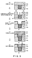
- FIGS. 1a and 1b a concrete structure of such a semiconductor device will be described below. These figures show a part of an example of a semiconductor device.
- FIG. 1a is a front-side sectional view of the semiconductor device
- FIG. 1b is a lateral-side sectional view of the semiconductor device.
- reference numbers 21 through 24 denote interlayer dielectric films of CF films having a thickness of, e.g., about 7000 angstroms.
- Reference numbers 25 and 26 denote wiring layers of Cu layers having a thickness of, e.g., about 7000 angstroms, and reference numbers 27 and 28 denote connection lines of W layers for connecting the Cu wiring layers 25 and 26 to each other.
- adhesion layers 29 having a thickness of, e.g., about 200 angstroms, are formed between the CF films 21 through 24 and the Cu wiring layers 25, 26 and W layers 27, 28, and between the W layers 27, 28 and the Cu wiring layers 25, 26.
- the adhesion layer 29 is expressed by a single thick line for convenience.
- This CF film 32a is formed by using, e.g., Ar (argon) gas, as a plasma gas, and, e.g., C 4 F 8 and C 2 H 4 gases, as deposition gases, to activate the deposition gases as plasmas in, e.g., an ECR plasma system (see FIG. 5 ) utilizing the ECR (electron cyclotron resonance) which will be described later.
- Ar argon
- C 4 F 8 and C 2 H 4 gases deposition gases
- a process for forming a wiring of W in the CF film 32 is carried out.
- a hole 33b for embedding W is first formed in a part of the surface of the CF film 32a, in which the wiring of W is intended to be formed, as shown in FIG. 2(b) .
- This hole 33a is formed by forming a predetermined pattern on the surface of the CF film 32a and by carrying out an etching process in an etching system (not shown).
- the surface of the CF film 32a is irradiated with the plasma of H 2 . That is, Ar gas and H 2 gas are introduced into, e.g., a plasma processing system (see FIG. 6 ), which will be described later, to activate H 2 gas as a plasma to irradiate with the plasma of H 2 for, e.g., about 5 seconds.
- the introduction of Ar gas is carried out in order to facilitate the production of the plasma of H 2 and in order to stabilize the plasma. If the irradiation with the plasma of H 2 is thus carried out, fluorine (F) in the surface layer portion of the CF film 32a reacts with H to fly away from the CF film 32a as HF. For that reason, although the amount of F decreases in the surface layer portion, carbon (C) remains, so that the concentration of C is high.
- a Ti (titanium) layer 34a having a thickness of, e.g., 200 angstroms, is formed on the whole surface of the CF film 32a as shown in FIG. 2(d) . That is, the Ti layer 34a is formed on the whole surface of the CF film 32a including the inner wall surface of the hole 33a by sputtering Ti of a target, e.g., by introducing Ar gas into, a sputtering system (see FIG. 7 ), which will be described later, while the interior of the system is heated at 300 °C or higher.
- Ti layer 34a is thus formed on the surface of the CF film 32a while heating the substrate 31, C in the surface layer portion of the CF film 32a reacts with Ti in the boundary between the CF film 32a and the Ti layer 34a to form a TiC (a compound containing Ti and C) film 34b having a thickness of, e.g., 50 angstroms, as shown in FIG. 4 .
- the Ti layer 34a and the TiC layer 34b constitute the adhesion layer 34.
- the Ti layer 34a is deposited while the interior of the sputtering system is heated at 300 °C or higher in the above described example.
- an annealing process may be carried out at a temperature of 400 °C or higher with respect to the substrate 31, on which the Ti layer 34a has been formed, after the Ti layer 34a has been deposited at a temperature of, e.g., about 300 °C.
- a process for forming a W layer 36 on the surface of the adhesion layer 34 to fill the hole 33a with W is carried out.
- a CMP process (polishing process) is carried out in a CMP system (not shown) to polish and remove an undesired portion of the Ti layer 34a on the surface of the CF film 32a, i.e., a portion of the Ti layer 34a other than the inner wall surface of the hole 33a, as shown in FIG. 2(f) .
- the hole 33a formed in the CF film 32a is filled with W via the Ti layer 34a to form a connection line of the W layer 36.
- a process for forming a Cu wiring layer on the surface of the CF film 32a, in which the connection line of W has been formed is carried out.
- a CF film 32b having a thickness of 7000 angstroms is first formed on the surface of the CF film 32a, in which the connection line of W has been formed, by the same method as that in FIG. 2(a) .
- a groove 33b is formed in the surface of the CF film, in which a wiring of Cu is intended to be formed, by the same method as that in FIG. 2(b) .
- this surface is irradiated with the plasma of H 2 .
- This process is carried out in, e.g., the same manner as that in FIG. 2(c) , to irradiate the surface with the plasma of H 2 for, e.g., about 5 seconds.
- an adhesion layer 37 comprising the Ti layer and the TiC layer is formed on the whole surface of the CF film 32b.
- This process is carried out in, e.g., the same manner as that in FIG. 2(d) , to form the adhesion layer 37 having a thickness of, e.g., 200 angstroms.
- a Cu layer (Cu wiring layer) 38 having a thickness of, e.g., about 7000 angstroms, is formed on the surface of the Ti layer 37.
- the surface is polished by a CMP system (not shown).
- an ECR plasma system for carrying out an ECR plasma process a plasma processing system for carrying out the irradiation with the plasma of H 2 , and a sputtering system for forming a Ti layer will be briefly described below.
- an ECR plasma system shown in FIG. 5 has a vacuum vessel 4 comprising a plasma chamber 4A and a deposition chamber 4B.
- a high frequency wave (microwave) M of, e.g., 2.45 GHz, is designed to be supplied into the vacuum vessel 4 from a high frequency power supply part 41 via a waveguide 42 and a transmission window 43.
- a magnetic field B extending from the plasma chamber 4A toward the deposition chamber 4B is formed by a main electromagnetic coil 44a and an auxiliary electromagnetic coil 44b, which are provided around the plasma chamber 4A and above and below the deposition chamber 4B, respectively.
- the intensity of the magnetic field B in the vicinity of an ECR point P is, e.g., 875 gausses. Then, by the interaction between the magnetic field B and the microwave M, an electron cyclotron resonance is caused at the ECR point P.
- a semiconductor wafer (which will be hereinafter referred to as a "wafer") 10 serving as a substrate is mounted on a supporting table 45 which is provided in the deposition chamber 4B, and a bias voltage is applied to the supporting table 45 by means of a high frequency power supply part 46.
- Ar gas serving as a plasma gas is introduced into the plasma chamber 4A via a plasma gas supply pipe 48, and a deposition gas is introduced into the deposition chamber 4B via a deposition gas supply part 49 to activate the deposition gas as a plasma by the electron cyclotron resonance.
- This system can carry out the irradiation with the plasma of H 2 .
- H 2 gas and Ar gas are introduced into the plasma chamber 4A to activate H 2 gas as a plasma by the electron cyclotron resonance.
- a system shown in FIG. 6 is a parallel plate plasma processing system for carrying out the irradiation with the plasma of H 2 .
- reference number 51 denotes a process chamber
- 52 denotes a supporting table which serves as a bottom electrode connected to a high frequency power supply part 53
- 54 denotes a grounded top electrode which is provided so as to face the supporting table 52.
- a wafer 10 is mounted on the supporting table 52, and a high frequency power is applied between the supporting table 52 and the top electrode 54 to produce plasma.
- H 2 gas and Ar gas are supplied into the process chamber 51 via a gas introducing pipe 56 at predetermined flow rates, respectively, to activate H 2 gas as a plasma to irradiate the surface of the CF film on the wafer 10 with the plasma of H 2 for, e.g., about 5 seconds.
- a system shown in FIG. 7 is a parallel plate plasma processing system for carrying out the deposition of the CF film.
- reference number 61 denotes a process chamber
- 62 denotes a supporting table which serves as a grounded bottom electrode
- 63 denotes a top electrode which is connected to a high frequency power supply part 64 and is provided so as to face the bottom electrode 62
- 65 denotes a target of Ti which is provided on the bottom surface of the top electrode 63.
- a high frequency power is applied between the supporting table 62 and the top electrode 63, while the interior of the process chamber 61 is heated at, e.g., 300 °C, to produce plasma.
- the CF films 32a and 32b which are insulating films, it is not required to provide any barrier layers for preventing Cu from diffusing into the insulating films, or it has only to provide a very thin barrier layer. Moreover, since the CF films 32a and 32b have a low relative dielectric constant of 2.5, it is possible to obtain a semiconductor device corresponding to the scale down and accelerating by using the CF films 32a and 32b as the insulating films.
- the adhesion layer is formed between the Cu wiring layer 38 and the CF films 32a, 32b in the semiconductor device according to the present invention, the adhesion between the CF films 32a, 32b and the Cu wiring layer 38 is enhanced, so that it is possible to inhibit the Cu wiring layer 38 from being peeled off from the CF films 32a and 32b. If a metal layer of Cu or the like is formed directly on the CF film, there is the possibility that F in the CF film reacts with the metal to form a metal fluoride in the boundary between the CF film and the metal layer.
- this metal fluoride generally has low sublimation and melting points, the metal fluoride is melted or sublimed if the substrate is heated to a temperature of the sublimation or melting point or higher in the subsequent process, so that there is the possibility that the metal fluoride is peeled off from the CF film.
- the TiC layer 34b is not peeled off from the CF films 32a and 32b. Because TiC is stable without being vaporized or melted even in a process, in which the substrate 31 is heated to a high temperature, since the TiC layer 34b formed between the Ti layer 34a and the CF films 32a, 32b has a high melting point of 3257 °C in an example of the adhesion layer 34 shown in FIG. 4 . The TiC layer 34b is not peeled off from the CF films 32a and 32b.
- the Ti layer 34a in the adhesion layer 34 is difficult to be peeled off from the Cu wiring layer 38 and the W layer 36 since these layers are metal layers. As a result, it is possible to inhibit the CF films 32a and 32b from being peeled off from the Cu wiring layer 38 and the W layer 36, so that it is possible to obtain a semiconductor device having high reliability.
- the Cu wiring layer 38 is electrically connected to the W layer 36 even if the TiC layer 34b exists between the CF film 32a, 32b and the Cu wiring layer 38. For that reason, when the Cu wiring layer 38 and the W layer 36 are formed, it is not required to peel off the TiC layer 34b.
- the metal of the adhesion layer may be W, Mo (molybdenum), Cr (chromium), Co (cobalt), Ta (tantalum), Nb (niobium) or Zr (zirconium) in place of Ti.
- fluorides of W or Mo have a melting point of 20 °C or less and fluorides of Cr and Co have a melting point of about 100°C or less, whereas carbon compounds of these metals have a melting point of about 2000 °C to about 4000 °C and carbon compounds of Ta, Nb and Zr have a very high melting point.
- this sample comprises a CF film having a thickness of 5000 angstroms, a Ti layer having a thickness of 500 angstroms, and a Cu layer having a thickness of 2000 angstroms which are deposited on a silicon substrate in that order (Example 1).
- the CF film and the Ti layer were produced as follows. First, Ar gas, C 4 F 8 gas and C 2 H 4 gas were introduced into the ECR plasma system shown in FIG. 5 , at flow rates of 150 sccm, 40 sccm and 30 sccm, respectively. Then, the CF film was deposited on the silicon substrate at a microwave power (the high frequency power supply part 41) of 2.7 kW at a bias power (the high frequency power supply part 46) of 1.5 kW at a substrate temperature of 400 °C.
- H 2 gas and Ar gas were introduced into the ECR plasma system at flow rates of 300 sccm and 30 sccm, respectively, to irradiate the surface of the CF film with the plasma of H 2 .
- the microwave power was 2700 W
- the bias power was 0 W.
- the sputtering system shown in FIG. 7 was used for introducing Ar gas at a flow rate of 50 sccm at a temperature of 300 °C to deposit the Ti layer on the surface of the CF film.
- the power of the high frequency power supply part 64 was 1200 W.
- Example 1 With respect to the sample (Example 1) thus obtained, the amounts of Cu, Ti, CF and Si were analyzed by the SIMS (secondary ion mass spectroscopy). The same analysis was carried out by the SIMS with respect to the sample after an annealing process was carried out at 425 °C for 1 hour. Moreover, as a comparative experiment, the same experiment was carried out with respect to a sample (Comparative Example 1) wherein the CF film of the sample in Example 1 was replaced with an SiO 2 film as shown in FIG. 9(a) .
- Example 1 and Comparative Example 1 are shown in FIGS. 8b and 8c and FIGS. 9b and 9c , respectively ( FIGS. 8b and 9b show the results of SIMS analysis after a thin-film deposition process, and FIGS. 8c and 9c show the results of SIMS analysis after an annealing process).
- the axis of abscissas denotes depths (unit: a.u.) in the sample, and the axis of ordinates denotes the number (counted number) of ions, such as Cu ions.
- Example 1 there were obtained the results of analysis that Cu and Ti exist at depths ( ⁇ about 3.8 a.u., ⁇ about 47 a.u.) corresponding to the Cu and Ti layers after the annealing process, whereas only C and F exist and Cu does not exist at depth (about 94 a.u. ⁇ ) corresponding to the CF film on the side of the Si substrate.
- depths ⁇ about 3.8 a.u., ⁇ about 47 a.u.
- this sample comprises a CF film having a thickness of 5000 angstroms, a Ti layer having a thickness of 50 angstroms, a Cu layer having a thickness of 2000 angstroms, and a TiN layer having a thickness of 200 angstroms, which are deposited on a silicon substrate in that order (Example 2).
- the silicon substrate was electrically connected to the TiN layer as shown in FIG. 10 . Then, a voltage of 1 MV/cm was applied to the sample while the silicon substrate was heated at 275 °C, and the time (which will be hereinafter referred to as MTTF") until the CF film was short-circuited (until 0.1 A/cm 2 ) was measured.
- reference number 71 denotes a power supply part
- 72 denotes an ampere meter. A portion between the silicon substrate and the power supply part 71 was grounded.
- Example 2 As a comparative experiment, the same experiment was carried out with respect to a sample (Comparative Example 2) wherein the CF film of the sample in Example 2 was replaced with an SiO 2 film having the same thickness as shown in FIG. 10 .
- the length of the MTTF depends on the degree of diffusion of Cu into the CF film and SiO 2 film which are insulating films. That is, if the MTTF is long, the amount of Cu diffusing into the insulating films is small, and the capacity for preventing the diffusion of Cu is high.
- the TiN layer was formed on the top face of the Cu layer in order to prevent the Cu layer from being oxidized.
- amorphous material means a microcrystal having a crystallite size of less than 50 to 100 angstroms.
- the CF film serving as the insulating film is amorphous and formed by a micro-crystal having a crystalline size of less than 50 to 100 angstroms, it is guessed that Cu is difficult to pass through the CF film so that the capacity for preventing the diffusion of Cu is high.
- the film density of the CF film serving as the insulating film is preferably 1.50 g/cm 3 or higher in order to further enhance the capacity for preventing the diffusion of Cu.
- the inventors have studied a process for increasing the density of a CF film by changing a bias power which is applied to the substrate 31 in the above described ECR plasma system. As a result, the relationship between the magnitude of the bias power and the density of the formed CF film is shown in FIG. 11a , so that it was confirmed that the denseness of the CF film increases as the bias power increases.
- the amount (concentration) of oxygen (O 2 ) in the CF film serving as the insulating film is preferably 3 atomic% or less in order to further improve the capacity for preventing the diffusion of Cu.
- the inventors have studied a process for adding O 2 to the CF film in order to improve the pressure resistance of the semiconductor device. As a result, it was observed that the amount of O 2 in the obtained CF film can be controlled by adding O 2 gas during a thin-film deposition process in the above described ECR plasma system, and that as shown in FIG. 12a , the amount of O 2 in the formed CF film increases as the amount of the added O 2 gas increases.
- the semiconductor device it is effective to add nitrogen (N 2 ) to the CF film from the point of view of the increase of hardness and heat resistance of the CF film serving as the insulating film, whereas the amount (concentration) of N 2 in the CF film is preferably 3 atomic% or less.
- the inventors have studied a process for adding N 2 to the CF film in order to improve the hardness and heat resistance of the CF film. As a result, it was observed that the amount of N 2 in the obtained CF film can be controlled by adding N 2 gas during a thin-film deposition process in the above described ECR plasma system, and that the amount of N 2 in the formed CF film increases as the amount of the added N 2 gas increases (see FIG. 13a ).
- the relative dielectric constant of the CN film is higher than that of the CF film, and the relative dielectric constant of the whole insulating film increases as the amount of the CN film increases, so that the amount of N 2 in the CF film is preferably 3 atomic% or less.
- the amount (concentration) of boron (B) in the CF film serving as the insulating film is preferably in the range of from 10 -3 atomic% to 1 atomic% in order to improve the capacity for preventing the diffusion of Cu.
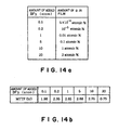
- the inventors have studied a process for adding B to the CF film in order to improve the pressure resistance of the semiconductor device. As a result, it was observed that the amount of B in the obtained CF film can be controlled by adding BF 3 gas during a thin-film deposition process in the above described ECR plasma system, and that as shown in FIG. 14a , the amount of B in the formed CF film increases as the amount of the added BF 3 gas increases.
- the MTTF was long when the amount of the added BF 3 gas was 10 sccm or less, particularly when the amount of the added BF 3 gas was in the range of from 0.2 sccm to 10 sccm.
- the amount of the added N 2 gas was 10 sccm
- the amount of B in the CF film was 1 atomic%
- the amount of the added N 2 gas was 0.2 sccm
- the amount of B was 10 -3 atomic%.
- the reason why the MTTF is long when the amount of B in the CF film is 1 atomic% or less is as follows. That is, if C having a dangling bond exists in the CF film, Cu is easy to be electrically attracted by the dangling bond, so that Cu is easy to diffuse into the CF film. Therefore, if B is added to the CF film, C having the dangling bond is bonded to B to increase the amount of the dangling bond. As a result, Cu is difficult to diffuse, and the MTTF increases. On the other hand, since the leak current decreases if the amount of B in the CF film is too large, it is guessed that the CF film is conductive, so that the MTTF is shortened.
- Example 3 The results in Example 3 are shown in FIG. 15a , and the results in Example 4 are shown in FIG. 15b .
- the axis of abscissas denotes depths (unit: a .u.) in the sample
- the axis of ordinates denotes the number (counted number) of ions, such as Cu ions. It can be seen from these results that the amounts of B in the CF film in Example 4 is greater than that in Example 3 to form a larger number of CB bonds, so that the MTTF in Example 4 is longer than that in Example 3.
- a semiconductor device may be formed as shown in FIG. 16 .
- reference numbers 81 through 84 denote interlayer dielectric films of CF films
- 85 and 86 denote Cu wiring layers.
- Connection lines for connecting the Cu wiring layers 85 and 86 to each other are formed of Cu layers 87 and 88.
- reference number 89 denotes adhesion layers which are formed between the CF films 81 through 84 and the Cu wiring layers 85 through 88.
- the above described irradiation with the plasma of H 2 may be carried out by, e.g., the ECR plasma system shown in FIG. 5 .
- the Ti layer may be deposited by the CVD (chemical vapor deposition) or the like.
- TiCl 4 gas and H 2 gas are used as deposition gases to form the Ti layer on the surface of the CF films by a chemical reaction TiCl 4 + H 2 ⁇ Ti + HCl.
Landscapes
- Engineering & Computer Science (AREA)
- Physics & Mathematics (AREA)
- Power Engineering (AREA)
- General Physics & Mathematics (AREA)
- Computer Hardware Design (AREA)
- Microelectronics & Electronic Packaging (AREA)
- Condensed Matter Physics & Semiconductors (AREA)
- Manufacturing & Machinery (AREA)
- Plasma & Fusion (AREA)
- Chemical & Material Sciences (AREA)
- Chemical Kinetics & Catalysis (AREA)
- Internal Circuitry In Semiconductor Integrated Circuit Devices (AREA)
- Formation Of Insulating Films (AREA)
Applications Claiming Priority (3)
| Application Number | Priority Date | Filing Date | Title |
|---|---|---|---|
| JP14058498A JP4355039B2 (ja) | 1998-05-07 | 1998-05-07 | 半導体装置及び半導体装置の製造方法 |
| JP14058498 | 1998-05-07 | ||
| PCT/JP1999/002363 WO1999057760A1 (fr) | 1998-05-07 | 1999-05-06 | Dispositif a semiconducteurs |
Publications (3)
| Publication Number | Publication Date |
|---|---|
| EP1077486A1 EP1077486A1 (en) | 2001-02-21 |
| EP1077486A4 EP1077486A4 (en) | 2003-08-13 |
| EP1077486B1 true EP1077486B1 (en) | 2011-08-03 |
Family
ID=15272098
Family Applications (1)
| Application Number | Title | Priority Date | Filing Date |
|---|---|---|---|
| EP99918319A Expired - Lifetime EP1077486B1 (en) | 1998-05-07 | 1999-05-06 | Semiconductor device |
Country Status (7)
| Country | Link |
|---|---|
| US (1) | US6720659B1 (ko) |
| EP (1) | EP1077486B1 (ko) |
| JP (1) | JP4355039B2 (ko) |
| KR (1) | KR100397314B1 (ko) |
| IL (1) | IL139532A0 (ko) |
| TW (1) | TW403942B (ko) |
| WO (1) | WO1999057760A1 (ko) |
Families Citing this family (26)
| Publication number | Priority date | Publication date | Assignee | Title |
|---|---|---|---|---|
| US8021976B2 (en) * | 2002-10-15 | 2011-09-20 | Megica Corporation | Method of wire bonding over active area of a semiconductor circuit |
| US6303423B1 (en) * | 1998-12-21 | 2001-10-16 | Megic Corporation | Method for forming high performance system-on-chip using post passivation process |
| US8178435B2 (en) * | 1998-12-21 | 2012-05-15 | Megica Corporation | High performance system-on-chip inductor using post passivation process |
| US6965165B2 (en) | 1998-12-21 | 2005-11-15 | Mou-Shiung Lin | Top layers of metal for high performance IC's |
| US7531417B2 (en) * | 1998-12-21 | 2009-05-12 | Megica Corporation | High performance system-on-chip passive device using post passivation process |
| JP2001044202A (ja) | 1999-07-30 | 2001-02-16 | Nec Corp | 半導体装置及びその製造方法 |
| US6759275B1 (en) | 2001-09-04 | 2004-07-06 | Megic Corporation | Method for making high-performance RF integrated circuits |
| DE10241154A1 (de) | 2002-09-05 | 2004-03-11 | Infineon Technologies Ag | Integrierte Schaltungsanordnung mit Zwischenmaterialien und zugehörige Komponenten |
| JP4413556B2 (ja) | 2003-08-15 | 2010-02-10 | 東京エレクトロン株式会社 | 成膜方法、半導体装置の製造方法 |
| US7776736B2 (en) | 2004-05-11 | 2010-08-17 | Tokyo Electron Limited | Substrate for electronic device capable of suppressing fluorine atoms exposed at the surface of insulating film from reacting with water and method for processing same |
| JP4555143B2 (ja) * | 2004-05-11 | 2010-09-29 | 東京エレクトロン株式会社 | 基板の処理方法 |
| JP2005347511A (ja) | 2004-06-03 | 2005-12-15 | Matsushita Electric Ind Co Ltd | 半導体装置及びその製造方法 |
| US8008775B2 (en) | 2004-09-09 | 2011-08-30 | Megica Corporation | Post passivation interconnection structures |
| US7355282B2 (en) | 2004-09-09 | 2008-04-08 | Megica Corporation | Post passivation interconnection process and structures |
| US8384189B2 (en) * | 2005-03-29 | 2013-02-26 | Megica Corporation | High performance system-on-chip using post passivation process |
| CN1901163B (zh) | 2005-07-22 | 2011-04-13 | 米辑电子股份有限公司 | 连续电镀制作线路组件的方法及线路组件结构 |
| JP5194393B2 (ja) * | 2006-06-23 | 2013-05-08 | 東京エレクトロン株式会社 | 半導体装置の製造方法 |
| JP4740071B2 (ja) * | 2006-08-31 | 2011-08-03 | 株式会社東芝 | 半導体装置 |
| US7585758B2 (en) * | 2006-11-06 | 2009-09-08 | International Business Machines Corporation | Interconnect layers without electromigration |
| JP5320570B2 (ja) * | 2006-11-09 | 2013-10-23 | 国立大学法人東北大学 | 層間絶縁膜、配線構造および電子装置と、それらの製造方法 |
| JP5261964B2 (ja) * | 2007-04-10 | 2013-08-14 | 東京エレクトロン株式会社 | 半導体装置の製造方法 |
| US7902641B2 (en) * | 2008-07-24 | 2011-03-08 | Tokyo Electron Limited | Semiconductor device and manufacturing method therefor |
| TWI510665B (zh) * | 2009-02-17 | 2015-12-01 | Tokyo Electron Ltd | 使用電漿反應製程來形成氟碳化物層的方法 |
| JP2009295992A (ja) * | 2009-07-29 | 2009-12-17 | Tokyo Electron Ltd | 半導体装置の製造方法、半導体装置 |
| JP2015195282A (ja) * | 2014-03-31 | 2015-11-05 | 東京エレクトロン株式会社 | 成膜方法、半導体製造方法及び半導体装置 |
| WO2022244095A1 (ja) * | 2021-05-18 | 2022-11-24 | キヤノンアネルバ株式会社 | 積層体及び積層体の製造方法 |
Family Cites Families (15)
| Publication number | Priority date | Publication date | Assignee | Title |
|---|---|---|---|---|
| JPS6373660A (ja) * | 1986-09-17 | 1988-04-04 | Fujitsu Ltd | 半導体装置 |
| US4960751A (en) * | 1987-04-01 | 1990-10-02 | Semiconductor Energy Laboratory Co., Ltd. | Electric circuit having superconducting multilayered structure and manufacturing method for same |
| JPH0574960A (ja) * | 1991-03-25 | 1993-03-26 | Fujitsu Ltd | 半導体装置の製造方法 |
| JPH05234987A (ja) * | 1992-02-24 | 1993-09-10 | Fujitsu Ltd | フッ素樹脂膜の形成方法 |
| US5559367A (en) * | 1994-07-12 | 1996-09-24 | International Business Machines Corporation | Diamond-like carbon for use in VLSI and ULSI interconnect systems |
| JP2748879B2 (ja) * | 1995-02-23 | 1998-05-13 | 日本電気株式会社 | フッ素化非晶質炭素膜材料の製造方法 |
| US5942328A (en) * | 1996-02-29 | 1999-08-24 | International Business Machines Corporation | Low dielectric constant amorphous fluorinated carbon and method of preparation |
| JP2956571B2 (ja) * | 1996-03-07 | 1999-10-04 | 日本電気株式会社 | 半導体装置 |
| JP3228183B2 (ja) * | 1996-12-02 | 2001-11-12 | 日本電気株式会社 | 絶縁膜ならびにその絶縁膜を有する半導体装置とその製造方法 |
| JPH10335461A (ja) * | 1997-04-02 | 1998-12-18 | Nec Corp | 半導体装置及び半導体装置の製造方法 |
| KR100295380B1 (ko) * | 1997-04-02 | 2001-08-07 | 가네꼬 히사시 | 층간절연물질로서저유전율의비정질탄소불화물막을가질수있는반도체장치및그제조방법 |
| JP3031301B2 (ja) * | 1997-06-25 | 2000-04-10 | 日本電気株式会社 | 銅配線構造およびその製造方法 |
| US6296780B1 (en) * | 1997-12-08 | 2001-10-02 | Applied Materials Inc. | System and method for etching organic anti-reflective coating from a substrate |
| US6159862A (en) * | 1997-12-27 | 2000-12-12 | Tokyo Electron Ltd. | Semiconductor processing method and system using C5 F8 |
| US6284657B1 (en) * | 2000-02-25 | 2001-09-04 | Chartered Semiconductor Manufacturing Ltd. | Non-metallic barrier formation for copper damascene type interconnects |
-
1998
- 1998-05-07 JP JP14058498A patent/JP4355039B2/ja not_active Expired - Fee Related
-
1999
- 1999-05-05 TW TW088107295A patent/TW403942B/zh not_active IP Right Cessation
- 1999-05-06 KR KR10-2000-7012346A patent/KR100397314B1/ko not_active IP Right Cessation
- 1999-05-06 IL IL13953299A patent/IL139532A0/xx not_active IP Right Cessation
- 1999-05-06 EP EP99918319A patent/EP1077486B1/en not_active Expired - Lifetime
- 1999-05-06 WO PCT/JP1999/002363 patent/WO1999057760A1/ja active IP Right Grant
-
2000
- 2000-09-12 US US09/660,884 patent/US6720659B1/en not_active Expired - Fee Related
Also Published As
| Publication number | Publication date |
|---|---|
| EP1077486A1 (en) | 2001-02-21 |
| TW403942B (en) | 2000-09-01 |
| JPH11330075A (ja) | 1999-11-30 |
| IL139532A0 (en) | 2001-11-25 |
| KR20010043347A (ko) | 2001-05-25 |
| KR100397314B1 (ko) | 2003-09-06 |
| WO1999057760A1 (fr) | 1999-11-11 |
| US6720659B1 (en) | 2004-04-13 |
| JP4355039B2 (ja) | 2009-10-28 |
| EP1077486A4 (en) | 2003-08-13 |
Similar Documents
| Publication | Publication Date | Title |
|---|---|---|
| EP1077486B1 (en) | Semiconductor device | |
| KR940010501B1 (ko) | 알킬 알루미늄 하이드라이드를 사용한 선택 퇴적을 이용한 퇴적막 형성 방법 | |
| US6436825B1 (en) | Method of copper barrier layer formation | |
| US5918149A (en) | Deposition of a conductor in a via hole or trench | |
| US6593660B2 (en) | Plasma treatment to enhance inorganic dielectric adhesion to copper | |
| JP3562628B2 (ja) | 拡散バリア膜、多層配線構造、およびそれらの製造方法 | |
| US6554914B1 (en) | Passivation of copper in dual damascene metalization | |
| US6150270A (en) | Method for forming barrier layer for copper metallization | |
| EP0425084A1 (en) | Process for forming deposited film by use of alkyl aluminum hydride | |
| US20070099417A1 (en) | Adhesion and minimizing oxidation on electroless CO alloy films for integration with low K inter-metal dielectric and etch stop | |
| US20040056366A1 (en) | A method of forming surface alteration of metal interconnect in integrated circuits for electromigration and adhesion improvement | |
| US6294458B1 (en) | Semiconductor device adhesive layer structure and process for forming structure | |
| US20050009320A1 (en) | Method of forming silicon carbide films | |
| US6713407B1 (en) | Method of forming a metal nitride layer over exposed copper | |
| US6391774B1 (en) | Fabrication process of semiconductor device | |
| EP0420597B1 (en) | Process for forming a deposited film by use of alkyl aluminum hydride and process for preparing semiconductor device | |
| KR100379308B1 (ko) | 불소 첨가 탄소막으로 이루어지는 절연막을 구비하는반도체 디바이스 및 그 제조 방법 | |
| US6424045B2 (en) | Semiconductor device with pure copper wirings and method of manufacturing a semiconductor device with pure copper wirings | |
| US20050277292A1 (en) | Method for fabricating low resistivity barrier for copper interconnect | |
| US7223692B2 (en) | Multi-level semiconductor device with capping layer for improved adhesion | |
| US6624062B2 (en) | Wiring structure in semiconductor device and method for forming the same | |
| JP3737366B2 (ja) | 半導体装置及びその製造方法 | |
| JP3266492B2 (ja) | 半導体装置の製造方法 | |
| KR100365061B1 (ko) | 반도체소자및반도체소자제조방법 | |
| JPH08325082A (ja) | 堆積膜形成法 |
Legal Events
| Date | Code | Title | Description |
|---|---|---|---|
| PUAI | Public reference made under article 153(3) epc to a published international application that has entered the european phase |
Free format text: ORIGINAL CODE: 0009012 |
|
| 17P | Request for examination filed |
Effective date: 20001121 |
|
| AK | Designated contracting states |
Kind code of ref document: A1 Designated state(s): BE DE FR IT |
|
| A4 | Supplementary search report drawn up and despatched |
Effective date: 20030701 |
|
| RIC1 | Information provided on ipc code assigned before grant |
Ipc: 7H 01L 23/532 B Ipc: 7H 01L 21/314 B Ipc: 7H 01L 21/768 A |
|
| 17Q | First examination report despatched |
Effective date: 20060825 |
|
| GRAP | Despatch of communication of intention to grant a patent |
Free format text: ORIGINAL CODE: EPIDOSNIGR1 |
|
| GRAS | Grant fee paid |
Free format text: ORIGINAL CODE: EPIDOSNIGR3 |
|
| GRAA | (expected) grant |
Free format text: ORIGINAL CODE: 0009210 |
|
| AK | Designated contracting states |
Kind code of ref document: B1 Designated state(s): BE DE FR IT |
|
| REG | Reference to a national code |
Ref country code: DE Ref legal event code: R096 Ref document number: 69943614 Country of ref document: DE Effective date: 20111006 |
|
| PG25 | Lapsed in a contracting state [announced via postgrant information from national office to epo] |
Ref country code: BE Free format text: LAPSE BECAUSE OF FAILURE TO SUBMIT A TRANSLATION OF THE DESCRIPTION OR TO PAY THE FEE WITHIN THE PRESCRIBED TIME-LIMIT Effective date: 20110803 |
|
| PG25 | Lapsed in a contracting state [announced via postgrant information from national office to epo] |
Ref country code: IT Free format text: LAPSE BECAUSE OF FAILURE TO SUBMIT A TRANSLATION OF THE DESCRIPTION OR TO PAY THE FEE WITHIN THE PRESCRIBED TIME-LIMIT Effective date: 20110803 |
|
| PLBE | No opposition filed within time limit |
Free format text: ORIGINAL CODE: 0009261 |
|
| STAA | Information on the status of an ep patent application or granted ep patent |
Free format text: STATUS: NO OPPOSITION FILED WITHIN TIME LIMIT |
|
| 26N | No opposition filed |
Effective date: 20120504 |
|
| REG | Reference to a national code |
Ref country code: DE Ref legal event code: R097 Ref document number: 69943614 Country of ref document: DE Effective date: 20120504 |
|
| REG | Reference to a national code |
Ref country code: FR Ref legal event code: ST Effective date: 20130131 |
|
| PG25 | Lapsed in a contracting state [announced via postgrant information from national office to epo] |
Ref country code: FR Free format text: LAPSE BECAUSE OF NON-PAYMENT OF DUE FEES Effective date: 20120531 |
|
| PGFP | Annual fee paid to national office [announced via postgrant information from national office to epo] |
Ref country code: DE Payment date: 20140430 Year of fee payment: 16 |
|
| REG | Reference to a national code |
Ref country code: DE Ref legal event code: R119 Ref document number: 69943614 Country of ref document: DE |
|
| PG25 | Lapsed in a contracting state [announced via postgrant information from national office to epo] |
Ref country code: DE Free format text: LAPSE BECAUSE OF NON-PAYMENT OF DUE FEES Effective date: 20151201 |