EP1061523B1 - Semiconductor memory device and electronic apparatus - Google Patents
Semiconductor memory device and electronic apparatus Download PDFInfo
- Publication number
- EP1061523B1 EP1061523B1 EP00302717A EP00302717A EP1061523B1 EP 1061523 B1 EP1061523 B1 EP 1061523B1 EP 00302717 A EP00302717 A EP 00302717A EP 00302717 A EP00302717 A EP 00302717A EP 1061523 B1 EP1061523 B1 EP 1061523B1
- Authority
- EP
- European Patent Office
- Prior art keywords
- signal
- refreshment
- circuit
- memory device
- semiconductor memory
- Prior art date
- Legal status (The legal status is an assumption and is not a legal conclusion. Google has not performed a legal analysis and makes no representation as to the accuracy of the status listed.)
- Expired - Lifetime
Links
Images


Classifications
-
- G—PHYSICS
- G11—INFORMATION STORAGE
- G11C—STATIC STORES
- G11C7/00—Arrangements for writing information into, or reading information out from, a digital store
- G11C7/10—Input/output [I/O] data interface arrangements, e.g. I/O data control circuits, I/O data buffers
- G11C7/1015—Read-write modes for single port memories, i.e. having either a random port or a serial port
- G11C7/1042—Read-write modes for single port memories, i.e. having either a random port or a serial port using interleaving techniques, i.e. read-write of one part of the memory while preparing another part
-
- G—PHYSICS
- G11—INFORMATION STORAGE
- G11C—STATIC STORES
- G11C11/00—Digital stores characterised by the use of particular electric or magnetic storage elements; Storage elements therefor
- G11C11/21—Digital stores characterised by the use of particular electric or magnetic storage elements; Storage elements therefor using electric elements
- G11C11/34—Digital stores characterised by the use of particular electric or magnetic storage elements; Storage elements therefor using electric elements using semiconductor devices
- G11C11/40—Digital stores characterised by the use of particular electric or magnetic storage elements; Storage elements therefor using electric elements using semiconductor devices using transistors
- G11C11/401—Digital stores characterised by the use of particular electric or magnetic storage elements; Storage elements therefor using electric elements using semiconductor devices using transistors forming cells needing refreshing or charge regeneration, i.e. dynamic cells
- G11C11/4063—Auxiliary circuits, e.g. for addressing, decoding, driving, writing, sensing or timing
- G11C11/407—Auxiliary circuits, e.g. for addressing, decoding, driving, writing, sensing or timing for memory cells of the field-effect type
- G11C11/409—Read-write [R-W] circuits
- G11C11/4096—Input/output [I/O] data management or control circuits, e.g. reading or writing circuits, I/O drivers or bit-line switches
-
- G—PHYSICS
- G11—INFORMATION STORAGE
- G11C—STATIC STORES
- G11C11/00—Digital stores characterised by the use of particular electric or magnetic storage elements; Storage elements therefor
- G11C11/21—Digital stores characterised by the use of particular electric or magnetic storage elements; Storage elements therefor using electric elements
- G11C11/34—Digital stores characterised by the use of particular electric or magnetic storage elements; Storage elements therefor using electric elements using semiconductor devices
- G11C11/40—Digital stores characterised by the use of particular electric or magnetic storage elements; Storage elements therefor using electric elements using semiconductor devices using transistors
- G11C11/401—Digital stores characterised by the use of particular electric or magnetic storage elements; Storage elements therefor using electric elements using semiconductor devices using transistors forming cells needing refreshing or charge regeneration, i.e. dynamic cells
- G11C11/406—Management or control of the refreshing or charge-regeneration cycles
- G11C11/40615—Internal triggering or timing of refresh, e.g. hidden refresh, self refresh, pseudo-SRAMs
-
- G—PHYSICS
- G11—INFORMATION STORAGE
- G11C—STATIC STORES
- G11C11/00—Digital stores characterised by the use of particular electric or magnetic storage elements; Storage elements therefor
- G11C11/21—Digital stores characterised by the use of particular electric or magnetic storage elements; Storage elements therefor using electric elements
- G11C11/34—Digital stores characterised by the use of particular electric or magnetic storage elements; Storage elements therefor using electric elements using semiconductor devices
- G11C11/40—Digital stores characterised by the use of particular electric or magnetic storage elements; Storage elements therefor using electric elements using semiconductor devices using transistors
- G11C11/401—Digital stores characterised by the use of particular electric or magnetic storage elements; Storage elements therefor using electric elements using semiconductor devices using transistors forming cells needing refreshing or charge regeneration, i.e. dynamic cells
- G11C11/406—Management or control of the refreshing or charge-regeneration cycles
- G11C11/40618—Refresh operations over multiple banks or interleaving
-
- G—PHYSICS
- G11—INFORMATION STORAGE
- G11C—STATIC STORES
- G11C11/00—Digital stores characterised by the use of particular electric or magnetic storage elements; Storage elements therefor
- G11C11/21—Digital stores characterised by the use of particular electric or magnetic storage elements; Storage elements therefor using electric elements
- G11C11/34—Digital stores characterised by the use of particular electric or magnetic storage elements; Storage elements therefor using electric elements using semiconductor devices
- G11C11/40—Digital stores characterised by the use of particular electric or magnetic storage elements; Storage elements therefor using electric elements using semiconductor devices using transistors
- G11C11/401—Digital stores characterised by the use of particular electric or magnetic storage elements; Storage elements therefor using electric elements using semiconductor devices using transistors forming cells needing refreshing or charge regeneration, i.e. dynamic cells
- G11C11/4063—Auxiliary circuits, e.g. for addressing, decoding, driving, writing, sensing or timing
- G11C11/407—Auxiliary circuits, e.g. for addressing, decoding, driving, writing, sensing or timing for memory cells of the field-effect type
- G11C11/4072—Circuits for initialization, powering up or down, clearing memory or presetting
-
- G—PHYSICS
- G11—INFORMATION STORAGE
- G11C—STATIC STORES
- G11C11/00—Digital stores characterised by the use of particular electric or magnetic storage elements; Storage elements therefor
- G11C11/21—Digital stores characterised by the use of particular electric or magnetic storage elements; Storage elements therefor using electric elements
- G11C11/34—Digital stores characterised by the use of particular electric or magnetic storage elements; Storage elements therefor using electric elements using semiconductor devices
- G11C11/40—Digital stores characterised by the use of particular electric or magnetic storage elements; Storage elements therefor using electric elements using semiconductor devices using transistors
- G11C11/401—Digital stores characterised by the use of particular electric or magnetic storage elements; Storage elements therefor using electric elements using semiconductor devices using transistors forming cells needing refreshing or charge regeneration, i.e. dynamic cells
- G11C11/4063—Auxiliary circuits, e.g. for addressing, decoding, driving, writing, sensing or timing
- G11C11/407—Auxiliary circuits, e.g. for addressing, decoding, driving, writing, sensing or timing for memory cells of the field-effect type
- G11C11/408—Address circuits
-
- G—PHYSICS
- G11—INFORMATION STORAGE
- G11C—STATIC STORES
- G11C7/00—Arrangements for writing information into, or reading information out from, a digital store
- G11C7/10—Input/output [I/O] data interface arrangements, e.g. I/O data control circuits, I/O data buffers
- G11C7/1051—Data output circuits, e.g. read-out amplifiers, data output buffers, data output registers, data output level conversion circuits
- G11C7/1063—Control signal output circuits, e.g. status or busy flags, feedback command signals
-
- G—PHYSICS
- G11—INFORMATION STORAGE
- G11C—STATIC STORES
- G11C7/00—Arrangements for writing information into, or reading information out from, a digital store
- G11C7/10—Input/output [I/O] data interface arrangements, e.g. I/O data control circuits, I/O data buffers
- G11C7/1078—Data input circuits, e.g. write amplifiers, data input buffers, data input registers, data input level conversion circuits
- G11C7/109—Control signal input circuits
-
- G—PHYSICS
- G11—INFORMATION STORAGE
- G11C—STATIC STORES
- G11C7/00—Arrangements for writing information into, or reading information out from, a digital store
- G11C7/20—Memory cell initialisation circuits, e.g. when powering up or down, memory clear, latent image memory
-
- G—PHYSICS
- G11—INFORMATION STORAGE
- G11C—STATIC STORES
- G11C8/00—Arrangements for selecting an address in a digital store
- G11C8/04—Arrangements for selecting an address in a digital store using a sequential addressing device, e.g. shift register, counter
-
- G—PHYSICS
- G11—INFORMATION STORAGE
- G11C—STATIC STORES
- G11C8/00—Arrangements for selecting an address in a digital store
- G11C8/18—Address timing or clocking circuits; Address control signal generation or management, e.g. for row address strobe [RAS] or column address strobe [CAS] signals
Definitions
- the present invention relates to a semiconductor memory device, such as a DRAM (Dynamic Random Access Memory), which needs to be refreshed for retaining data, an electronic apparatus which uses such a semiconductor memory device, and a semiconductor memory device which is suitable as a semiconductor memory device for saving data therein, for example, used in such an electronic apparatus.
- a semiconductor memory device such as a DRAM (Dynamic Random Access Memory)
- DRAM Dynamic Random Access Memory
- a DRAM has been used as a main storage memory of a personal computer, a server or the like until now, an era in which a large-capacity DRAM is used in a simple terminal such as a cellular phone is coming due to progress of Internet technology, mobile technology and so forth.
- a SRAM Static Random Access Memory
- a simple terminal such as a cellular phone.
- a DRAM Dynamic Random Access Memory
- a DRAM and a SRAM are used together, it is necessary to consider that the DRAM needs to be refreshed for retaining data, different from the SRAM.
- a DRAM mounted in a simple terminal such as a cellular phone be such that control of the DRAM by a controller can be easily performed
- a simple terminal such as a cellular phone is such that, when a main battery goes dead, or is removed, and, thereby, power supply by the main battery is stopped, power consumption of a backup battery due to refreshment of the DRAM can be reduced as much as possible.
- the present invention has been devised in consideration of the above-mentioned point, and a first aim of preferred embodiments is to provide a semiconductor memory device performing a refresh operation for retaining data, and control of which by a controller is easy.
- a second aim is to provide an electronic apparatus which is provided with a semiconductor memory device performing a refresh operation for retaining data and a controller, and, in which control of the semiconductor memory device by the controller is easy.
- a third aim is to provide a semiconductor memory device such that saving of data, from another semiconductor memory device, in the semiconductor memory device can be easily performed.
- a fourth aim is to provide a semiconductor memory device such that saving of data from the semiconductor memory device is easy.
- US 4,758,993 describes a dynamic random access memory (DRAM) device formed on a semiconductor substrate, the device having an array of memory cells which are divided in several sub-arrays.
- the device has memory blocks each containing one of the sub-arrays, a word decoder and a column decoder.
- Each of the memory blocks is selected independently to perform an access operation and refresh operation.
- a comparison circuit detects double selection and gives priority to one of the operations. The operation selected is thus preferentially performed.
- the refresh operations is then performed.
- the access operation is performed preferentially. Further, a complicated operation for priority selection may be performed according to a predetermined schedule memorized in a priority providing means.
- a common word bus line is proposed for accessing each of the memory blocks, namely, each sub-array, in order to reduce the number of common word lines for realizing a further high packing density of the DRAM device.
- US 5,675,770 discloses a memory controller having means for comparing a designated address with addresses setting an area in a memory. It is desired to utilize two (or more) non-contiguous areas in memory as though they are formed as a single continuous area. An end address of a first memory area and a start address of a second memory area are set in a setting means. When the address in an address counter reaches the end address of the first of the two (or more) memory areas, the address counter is controlled to jump directly to the start address of the second area. By virtue of this structure, it has become possible to access the first and second areas successively, as one continuous area, even though the two areas are separated from each other in the memory space.
- a semiconductor memory device performing a refresh operation for retaining data, comprises:
- the semiconductor memory device according to the first aspect of the present invention is applied to a semiconductor memory device, which performs a refresh operation for retaining data, of an electronic apparatus including the semiconductor memory device and a controller which controls the semiconductor memory device, because the controller can recognize whether or not it is the time for the refresh operation, control of the semiconductor memory device by the controller can be easily performed.
- the controller can recognize whether or not it is the time for the refresh operation of the semiconductor memory device, control of the semiconductor memory device by the controller can be easily performed.
- the automatic writing portion which, when automatic writing is externally instructed to be performed, automatically writes data to the device in internally generated addresses is provided with, saving of the data of a first semiconductor memory device can be easily performed when an electronic apparatus including the first semiconductor memory device and a controller for controlling the first semiconductor memory device is provided with a second semiconductor memory device for saving therein the data stored in the first semiconductor memory device and the third aspect of the present invention is used as the second semiconductor memory device, for example.
- a semiconductor memory device comprises an automatic reading portion which comprises:
- the automatic reading portion which automatically reads data from the device when automatic reading is externally instructed to be performed and the access-accepting allowing/rejecting signal indicates that the data transfer destination agrees to accept access is provided with, it is possible to easily transfer data to (save data in) the data transfer destination (data saving destination), which outputs the access-accepting allowing/rejecting signal, when it is necessary to transfer the data (it is necessary to save the data, for example).
- FIGS.1 through 45 examples and embodiments according to the present invention of a semiconductor memory device and examples and embodiments according to the present invention of an electronic apparatus will now be described. now be described.
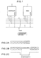
- FIG. 1 is a circuit diagram showing an essential portion of a first example of an electronic apparatus.
- this electronic apparatus includes a DRAM 1, a controller 2 which controls the DRAM 1, and buses such a command bus, an address bus, a data bus and so forth.
- the DRAM 1 is configured to self-manage refreshment of itself, and, when the time for refreshing itself comes, outputs a busy signal BUSY1 to a BUSY1 signal line 4, generates a refreshment address through an internal circuit thereof, performs the refreshment thereof, and, when finishing the refreshment, negates the busy signal BUSY1.
- the controller 2 is configured to be able to receive the busy signal BUSY1 output to the BUSY1 signal line 4 by the DRAM 1, and, when receiving the busy signal BUSY1, stop accessing the DRAM 1 until the busy signal BUSY1 is negated, for example.
- to output the busy signal BUSY1 means to cause the busy signal BUSY1 to have an L level
- to negate the busy signal BUSY1 means to cause the busy signal BUSY1 to have an H level
- FIGS. 2A, 2B and 2C are time charts showing an example of operations of the DRAM 1 and controller 2.
- FIG. 2A shows commands planned to be output from the controller 2
- FIG. 2B shows commands actually output from the controller 2
- FIG. 2C shows the busy signal BUSY1 output from the DRAM 1.
- this example shows a case where, in a case where the controller 2 plans to output commands C1 through C7 successively, the commands C1 through C4 are actually output, and the busy signal BUSY1 is output from the DRAM 1 when the command C4 is being output.
- the DRAM 1 because the DRAM 1 has already input the command C4 thereto when outputting the busy signal BUSY1, the DRAM 1 operates so as to perform refreshment thereof after executing the command C4, and negate the busy signal BUSY1 when finishing the refreshment.
- the controller 2 when receiving the busy signal BUSY1, the controller 2 stops outputting the commands C5 and the subsequent ones, stops accessing the DRAM 1, and, when the busy signal BUSY1 is negated, the controller 2 outputs the commands C5 and the subsequent ones successively, and restarts accessing the DRAM 1.
- the DRAM 1 is configured to self-manage refreshment of itself, outputs the busy signal BUSY1 to the BUSY1 signal line 4 when the time for refreshing itself comes, and, also, to generate a refreshment address through the internal circuit thereof and performs the refreshment thereof. Accordingly, the controller 2 does not need to manage refreshment of the DRAM 1.
- controller 2 it is possible for the controller 2 to recognize that the time for the refreshment of the DRAM 1 is occurring, as a result of receiving the busy signal BUSY1, and to stop accessing the DRAM 1. Accordingly, control of accessing the DRAM 1 by the controller 2 is easy.
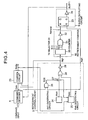
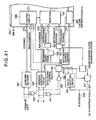
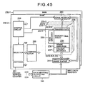
- FIG. 3 is circuit diagram of an essential portion of a first example of a semiconductor memory device.
- the first embodiment of the semiconductor memory device according to the present invention can be used as the DRAM 1 shown in FIG. 1 .
- the semiconductor memory device includes a command decoder 5 which inputs command signals from a controller thereto and decodes them, an address inputting circuit 6 which inputs address signals A0 through An thereto, holds and outputs them, and a data inputting/outputting circuit 7 performing inputting/outputting of write data/read data DQO through DQn.
- the semiconductor memory device further includes a refreshment control circuit 8 which controls the refreshment of the semiconductor memory device, a BUSY1 outputting circuit 9 which is controlled by the refreshment control circuit 8 and outputs the busy signal BUSY1. a refreshment counter 10 which is controlled by the refreshment control circuit 8 and outputs the refreshment address.
- the semiconductor memory device further includes memory areas 11-0 and 11-1 called banks to be selected by a bank address signal.
- the circuit arrangement of the bank 11-0 is the same as that of the bank 11-1.
- the bank 11-0 includes memory areas 12-0 through 12-3 called blocks.
- the blocks 12-0 through 12-3 each has the same circuit arrangement.
- the block 12-0 includes a memory cell array 13 in which memory cells are arranged, a row decoder 14 which decodes row address signals and selects a word line, a sense amplifier 15 which amplifies data read from the memory cell array 13, and a column decoder 16 which decodes column address signals and selects a column.
- the bank 11-0 further includes a data bus 17 which is used by the blocks 12-0 through 12-3 in common, write amplifier/sense buffer 18 which is provided for the blocks 12-0 through 12-3 in common, and a control circuit 19 which controls the bank 11-0.
- the bank 11-0 further includes a selector 20 which is controlled by the control circuit 19 and selects the row address signals output from the address inputting circuit 6 at the time of reading/writing of data, and selects the refreshment address output from the refreshment counter 10 at the time of the refreshment of the semiconductor memory device, and an address latch circuit 21 which holds and outputs the address signals output from the selector 20.
- a selector 20 which is controlled by the control circuit 19 and selects the row address signals output from the address inputting circuit 6 at the time of reading/writing of data, and selects the refreshment address output from the refreshment counter 10 at the time of the refreshment of the semiconductor memory device, and an address latch circuit 21 which holds and outputs the address signals output from the selector 20.
- FIG. 4 is a circuit diagram showing arrangements of the refreshment control circuit 8, BUSY1 outputting circuit 9 and refreshment counter 10.
- An internal command signal Com is obtained as a result of external command signals being decoded.
- a control circuit 23 is included in the bank 11-1.
- An RAS activating signal activates a circuit for RAS.
- the refreshment is performed for each row address in the order of the banks 11-0, 11-1 alternately.
- the refreshment control circuit 8 includes a Ref1 generating circuit which generates a refreshment control signal Ref1 which informs of the time for the refreshment of the semiconductor memory device periodically.
- management of the time for the refreshment of the semiconductor memory device may be performed as a result of an oscillator being mounted in the first example of the semiconductor memory device and the time being measured using the output of the oscillator.
- management of the time for the refreshment of the semiconductor memory device may be performed as a result of the time being measured using a clock signal from a crystal oscillator or the like provided in an electronic apparatus which uses the first example of the semiconductor memory device
- the refreshment control circuit 8 further includes a Refz generating circuit 25 which generates a refreshment control signal Refz for delaying commencement of the operation of the refreshment counter 10 until a command is executed, for giving priority to execution of the command, when outputting of the busy signal BUSY1 and outputting of the command from the controller are performed simultaneously.
- a Refz generating circuit 25 which generates a refreshment control signal Refz for delaying commencement of the operation of the refreshment counter 10 until a command is executed, for giving priority to execution of the command, when outputting of the busy signal BUSY1 and outputting of the command from the controller are performed simultaneously.
- the refreshment control circuit 8 further includes a NAND circuit 26 which processes, in accordance with the NAND manner, the internal command signal Com output from the command decoder 5 and the refreshment control signal Ref1, and a NMOS transistor 27, turning on, off of which is controlled by the output S26 of the NAND circuit 26.
- the refreshment control circuit 8 further includes a NOR circuit 28 which processes, in accordance with the NOR manner, the refreshment control signal Ref1 provided via the NMOS transistor 27 and the refreshment control signal Refz, and an inverter 29 which inverts the output of the NOR circuit 28 and outputs a refreshment control signal REF.
- the refreshment counter 10 includes a counter 30 which starts a counting operation using the refreshment control signal REF as a trigger signal and outputs the refreshment address, and a NAND circuit 31 which processes, in accordance with the NAND manner, the outputs of the counter 30, and an inverter 32 which inverts the output of the NAND circuit 31 and outputs a refreshment ending signal Ref-end which informs of the end of the refreshment.
- the BUSY1 outputting circuit 9 includes a RS flip-flop circuit 33 inputs thereto the refreshment control signal Ref1 as a setting signal and the refreshment ending signal Ref-end as a resetting signal, and an inverter 34 which inverts the positive-phase output Q of RS flip-flop circuit 33 and outputs the busy signal BUSY1.
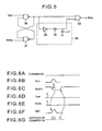
- FIG. 5 is a circuit diagram showing an arrangement of the Refz generating circuit 25.
- the Refz generating circuit 25 includes NAND circuits 36 and 37 which form a flip-flop circuit, and an inverting and delaying circuit 38 which inverts and delays the output of the NAND circuit 36.
- the inverting and delaying circuit 38 includes an inverter 39, a resistor 40 and a capacitor 41.
- the Refz generating circuit 25 further includes a NOR circuit 42 which processes, in accordance with the NOR manner, the output of the NAND circuit 36 and the output of the inverting and delaying circuit 38, and outputs the refreshment control signal Refz.
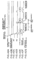
- FIGS. 6A through 6G show waveforms illustrating a first example of operations of the refreshment control circuit 8, BUSY1 outputting circuit 9 and refreshment counter 10.
- FIG. 6A shows commands output from the controller
- FIG. 6B shows the refreshment control signal Ref1
- FIG. 6C shows the busy signal BUSY1
- FIG. 6D shows the internal command signal Com
- FIG. 6E shows the RAS activating signal RASz
- FIG. 6F shows the refreshment control signal REF
- FIG. 6G shows the outputs of the counter 30.
- FIGS. 6A through 6G show a case where the refreshment control signal Ref1 is output from the Ref1 generating circuit 24 (the refreshment control signal Ref1 is caused to have the H level) when no commands are output from the controller.
- the reset RS flip-flop circuit 33 is set by the refreshment control signal Ref1, the positive-phase output Q of the RS flip-flop circuit 33 comes to have the H level, and the busy signal BUSY1 is output (the busy signal BUSY1 comes to have the L level).
- the internal command signal Com has the L level
- the output S26 of the NAND circuit 26 has the H level
- the NMOS transistor 27 is turned on
- the RAS activating signal RASz has the L level
- the output of the NAND circuit 37 has the H level
- the output of the NAND circuit 36 has the L level
- the output of the inverting and delaying circuit 38 has the H level
- the refreshment control signal Refz has the L level.
- the refreshment control signal Ref1 output from the Ref1 generating circuit 24 is provided to the NOR circuit 28 via the NMOS transistor 27.
- the NOR circuit 28 functions as an inverter for the refreshment control signal Ref1 the refreshment control signal Ref1 is output as the refreshment control signal REF, and the counter 30 is started.
- the refreshment address is output from the counter 30 immediately after the busy signal BUSY1 is caused to have the L level, and the refreshment of the semiconductor memory device is performed.
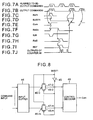
- FIGS. 7A through 7J show waveforms illustrating a second example of operations of the refreshment control circuit 8, BUSY1 outputting circuit 9 and refreshment counter 10.
- FIG. 7A shows commands planned to be output from the controller
- FIG. 7B shows the commands actually output from the controller
- FIG. 7C shows the refreshment control signal Ref1
- FIG. 7D shows the busy signal BUSY1
- FIG. 7E shows the internal command signal Com
- FIG. 7F shows the RAS activating signal RASz
- FIG. 7G shows the output S26 of the NAND circuit 26
- FIG. 7H shows the refreshment control signal Refz
- FIG. 7I shows the refreshment control signal REF
- FIG. 7J shows the outputs of the counter 30.
- FIGS. 7A through 7J show a case where inputting of the command from the controller and outputting of the refreshment control signal Ref1 are performed simultaneously. Specifically, in the case where the commands C1, C2 and C3 are planned to be output successively from the controller, inputting of the command C1 and outputting of the refreshment control signal Ref1 are performed simultaneously.
- the reset RS flip-flop circuit 33 is set by the refreshment control signal Ref1, the positive-phase output Q of the RS flip-flop circuit 33 comes to have the H level, and the busy signal BUSY1 is output (the busy signal BUSY1 comes to have the L level).
- the internal command signal Com comes to have the H level
- the output of the NAND circuit 26 comes to have the L level
- the NMOS transistor 27 is turned off.
- the refreshment control signal Ref1 is not provided to the NOR circuit 28.
- the refreshment control signal Ref1 comes to have the L level
- the output of the NAND circuit 26 come to have the H level
- the NMOS transistor 27 is turned on
- the NOR circuit 28 functions as an inverter for the refreshment control signal Refz.
- the refreshment control signal Refz is output as the refreshment control signal REF.
- the output of the NAND circuit 36 comes to have the H level
- the refreshment control signal Refz come to have the L level
- the output of the inverting and delaying circuit 38 comes to have the H level
- the L level of the refreshment control signal Refz is maintained, in the Refz generating circuit 25.
- the RAS activating signal RASz comes to have the H level.
- the RAS activating signal RASz come to have the L level.
- the output of the NAND circuit 37 comes to have the H level
- the output of the NAND circuit 36 comes to have the L level
- the refreshment control signal Refz come to have the H level
- the output of the inverting and delaying circuit 38 comes to have the H level
- the refreshment control signal Refz comes to have the L level, in the Refz generating circuit 25.
- the busy signal BUSY1 comes to have the L level.
- the refreshment addresses are output from the counter 30 after execution of the command C1 is finished, and the refreshment is performed.
- the output of the NAND circuit 31 comes to have the L level
- the refreshment ending signal Ref-end comes to have the H level
- the RS flip-flop circuit 33 is reset by the refreshment ending signal Ref-end
- the positive-phase output Q of the RS flip-flop circuit 33 comes to have the L level
- the busy signal BUSY1 comes to have the H level
- the busy signal BUSY1 is negated.
- FIG. 8 is a circuit diagram showing an arrangement of the command decoder 5.
- the command decoder 5 includes an input buffer 44 which causes the command signals from the controller to undergo buffering, and an inverter 45 which inverts the busy signal BUSY1.
- the command decoder 5 further includes transmission gates 46-0, ⁇ ⁇ ⁇ , 46-m which control transmission of a command output from the input buffer 44.
- the transmission gates 46-0, ⁇ ⁇ ⁇ , 46-m include NMOS transistors 47-0, ⁇ ⁇ ⁇ , 47-m, turning on, off thereof being controlled by the busy signal BUSY1, and PMOS transistors 48-0, ⁇ ⁇ ⁇ , 48-m, turning on, off thereof being controlled by the output of the inverter 45.
- the transmission gates 46-1, ⁇ ⁇ ⁇ , 46-(m - 1) provided between the transmission gates 46-0 and 46-m are not shown in the figure.
- the transmission gates 46-0, ⁇ ⁇ ⁇ , 46-m are turned on when the busy signal BUSY1 has the H level, and are turned off when the busy signal BUSY1 has the L level. Thereby, when a command is output from the controller during the time for the refreshment of the semiconductor memory device, the command signals are not brought in.
- the command decoder 5 further includes a control decoder 49 which decodes the command signals provided via the transmission gates 46-0, ⁇ ⁇ ⁇ , 46-m from the input buffer 44, and outputs the internal command signal Com.
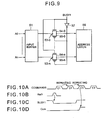
- FIG. 9 is a circuit diagram showing an arrangement of the address inputting circuit 6.
- the address inputting circuit 6 includes an input buffer 51 which causes the address signals A0 through An from the controller to undergo buffering, and an inverter 52 which inverts the busy signal BUSY1.
- the address inputting circuit 6 further includes transmission gates 53-0, ⁇ ⁇ ⁇ , 53-n which control transmission of the address signals A0 through An output from the input buffer 51.
- the transmission gates 53-0, ⁇ ⁇ ⁇ , 53-n include NMOS transistors 54-0, ⁇ ⁇ ⁇ , 54-n, turning on, off thereof being controlled by the busy signal BUSY1, and PMOS transistors 55-0, ⁇ ⁇ ⁇ , 55-n, turning on, off thereof being controlled by the output of the inverter 52.
- the transmission gates 53-1, ⁇ ⁇ ⁇ , 53-(n - 1) provided between the transmission gates 53-0 and 53-n are not shown in the figure.
- the transmission gate 53-0, ⁇ ⁇ ⁇ , 53-n are turned on when the busy signal BUSY1 has the H level, and are turned off when the busy signal BUSY1 has the L level. Thereby, when the address signals A0 through An are output from the controller during the time for the refreshment of the semiconductor memory device, the address signals A0 through An are not brought in.
- the address inputting circuit 6 further includes an address latch circuit 56 which holds and outputs the address signals A0 through An provided via the transmission gates 53-0, ⁇ ⁇ ⁇ , 53-n from the input buffer 51.
- the refreshment of the semiconductor memory device is managed by the refreshment control circuit 8. Then, when the time for the refreshment of the semiconductor memory device comes and there is no command which is being processed, the refreshment of the semiconductor memory device can be performed based on the refreshment address output from the refreshment counter 10 immediately. When the time for the refreshment of the semiconductor memory device comes but there is a command which is being processed, the refreshment of the semiconductor memory device can be performed based on the refreshment address output from the - refreshment counter 10 after the command is executed. Accordingly, the controller does not need to manage the refreshment of the semiconductor memory device.
- the busy signal BUSY1 is output from the BUSY1 outputting circuit 9 when the time for the refreshment of the semiconductor memory device comes. Therefore, the controller can recognize that the time for the refreshment of the semiconductor memory device comes, as a result of receiving the busy signal BUSY1. Accordingly, control of access to the semiconductor memory device by the controller is easy.
- the command decoder 5 is controlled so as not to bring any command in, and the address inputting circuit 6 is controlled so as not to bring any address signals in, while the busy signal BUSY1 is being output. Therefore, the controller may output the same command repeatedly which is not brought in by the semiconductor memory device, while the busy signal BUSY1 is being output, as shown in FIGS. 10A through 10D.
- FIG. 10A shows a command output from the controller
- FIG. 10B shows the refreshment control signal Ref1
- FIG. 10C shows the busy signal BUSY1
- FIG. 10D shows the internal command signal Com.
- FIG. 11 is a circuit diagram showing an essential portion of a first embodiment of a semiconductor memory device according to the present invention.
- the first embodiment of the semiconductor memory device according to the present invention can also be used as the DRAM 1 shown in FIG. 1 .
- the first embodiment of the semiconductor memory device according to the present invention includes a BUSY1a generating circuit 58 and a BUSY1b generating circuit 59 shown in FIG. 11 , which are not included in the first embodiment of the semiconductor memory device according to the present invention shown in FIG. 3 , and includes a command decoder 60 and an address inputting circuit 61, the circuit arrangements of which are different from those of the command decoder 5 and address inputting circuit 6 included in the first example of the semiconductor memory device shown in FIG. 3 . Except for those points, The first embodiment of the semiconductor memory device according to the present invention has the same arrangement as that of the first example of the semiconductor memory device shown in FIG. 3 .
- the BUSY1b generating circuit 59 inputs the busy signal BUSY1 thereto, and outputs a busy signal BUSY1b. As shown in FIG. 14E , the level of the busy signal BUSY1b changed from the H level to the L level when the level of the busy signal BUSY1 changes from the L level to the H level, and, after a fixed time period elapses, the level of the busy signal BUSY1b changes to the H level.
- the BUSY1a generating circuit 58 inputs the busy signals BUSY1 and BUSY1b thereto, and outputs a busy signal BUSY1a. As shown in FIG. 14D , when the level of the busy signal BUSY1 changes from the H level to the L level, the level of the busy signal BUSY1a changes from the H level to the L level, and, then, when the level of the busy signal BUSY1b changes from the L level to the H level, the level of the busy signal BUSY1a changes from the L level to the H level.
- FIG. 12 is a circuit diagram showing an arrangement of the command decoder 60.
- the command decoder 60 includes an input buffer 63 which causes command signals from the controller to undergo buffering, control decoder 64 which decodes the command signals output from the input buffer 63 and outputs the internal command signal Com, and a register 65 which temporarily stores the command.
- the command decoder 60 further includes a changeover switch circuit 66, the operation of which is controlled by the busy signal BUSY1a.
- the changeover switch circuit 66 transmits the command signals output from the input buffer 63 to the control decoder 64.
- the changeover switch circuit 66 transmits the command signals output from the input buffer 63 to the register 65.
- the command decoder 60 further includes a connecting switch circuit 67, the operation of which is controlled by the busy signal BUSY1b.
- the connecting switch circuit 67 When the busy signal BUSY1b has the L level, the connecting switch circuit 67 is turned on and provides the command signals temporarily stored in the register 65 to the control decoder 64. When the busy signal BUSY1b has the H level, the connecting switch circuit 67 is turned off.
- FIG. 13 is a circuit diagram showing an arrangement of the address inputting circuit 61.
- the address inputting circuit 61 includes an input buffer 69 which causes the address signals A0 through An from the controller to undergo buffering, an address latch circuit 70 which holds and outputs the address signals A0 through An, and a register 71 which temporarily stores the address signals A0 through An.
- the address inputting circuit 61 further includes a changeover switch circuit 72, the operation of which is controlled by the busy signal BUSY1a.
- the changeover switch circuit 72 transmits the address signals A0 through An output from the input buffer 69 to the address latch circuit 70.
- the changeover switch circuit 72 transmits the address signals A0 through An output from the input buffer 69 to the register 71.
- the address inputting circuit 61 further includes a connecting switch circuit 73, the operation of which is controlled by the busy signal BUSY1b.
- the connecting switch circuit 73 When the busy signal BUSY1b has the L level, the connecting switch circuit 73 is turned on and provides the address signals A0 through An temporarily stored in the register 71 to the address latch circuit 70.
- the connecting switch circuit 73 When the busy signal BUSY1b has the H level, the connecting switch circuit 73 is turned off.
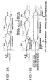
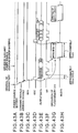
- FIGS. 14A through 14H show waveforms illustrating operations of the first embodiment of the semiconductor memory device according to the present invention.
- FIG. 14A shows commands output from the controller
- FIG. 14B shows the refreshment control signal Ref1
- FIG. 14C shows the busy signal BUSY1
- FIG. 14D shows the busy signal BUSY1a
- FIG. 14E shows the busy signal BUSY1b
- FIG. 14F shows the output of the input buffer 63 of the command decoder 60
- FIG. 14G shows the output of the register 65 of the command decoder 60
- FIG. 14H shows the RAS activating signal RASz.
- FIGS. 14A through 14H show a case where the refreshment control signal Ref1 is output from the Ref1 generating circuit 24 of the refreshment (otherwise known as a refresh) control circuit 8 after a command C1 is output from the controller, and, in response thereto, the busy signal BUSY1 is output from the BUSY1 outputting circuit 9, and, then, however, a command C2 is output from the controller after the command C1.
- the refreshment control signal Ref1 is output from the Ref1 generating circuit 24 of the refreshment (otherwise known as a refresh) control circuit 8 after a command C1 is output from the controller, and, in response thereto, the busy signal BUSY1 is output from the BUSY1 outputting circuit 9, and, then, however, a command C2 is output from the controller after the command C1.
- the command C1 is transmitted to the control decoder 64 via the input buffer 63 and changeover switch circuit 66 in the command decoder 60, and the command C1 is executed.
- the refreshment control signal Ref1 being output from the Ref1 generating circuit 24 of the refreshment control circuit 8
- the busy signal BUSY1 is output from the BUSY1 outputting circuit 9 (the BUSY1 signal is caused to have the L level) as shown in FIG. 14C , and the refreshment of the semiconductor memory device is performed after the command C1 is executed.
- the level of the busy signal BUSY1a changes from the H level to the L level, and the command C2 output from the controller is temporarily stored in the register 65 via the input buffer 63 and changeover switch circuit 66, in the command decoder 60.
- the level of the busy signal BUSY1 changes from the L level to the H level (the busy signal BUSY1 is negated), in response thereto, the level of the busy signal BUSY1b changes from the H level to the L level, the command C2 temporarily stored in the register 65 is provided to the control decoder 64 via the connecting switch circuit 67, and the command C2 is executed.
- the refreshment of the semiconductor memory device is managed by the refreshment control circuit 8. Then, when the time for the refreshment of the semiconductor memory device comes and there is no command which is being processed, the refreshment of the semiconductor memory device can be performed based on the refreshment address output from the refreshment (otherwise known as a refresh) canter 10 immediately. When the time for the refreshment of the semiconductor memory device comes but there is a command which is being processed, the refreshment of the semiconductor memory device can be performed based on the refreshment address output from the refreshment counter 10 after the command is executed. Accordingly, the controller does not need to manage the refreshment of the semiconductor memory device.
- the busy signal BUSY1 is output from the BUSY1 outputting circuit 9 when the time for the refreshment of the semiconductor memory device comes.
- the semiconductor memory device can accept command signals and address signals while the refreshment of the semiconductor memory device being performed. Accordingly, the controller can access the semiconductor memory device even while the refreshment of the semiconductor memory device is being performed, and, thus, efficient operations can be performed.
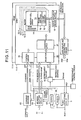
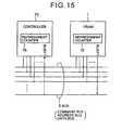
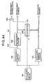
- FIG. 15 is a circuit diagram showing an essential portion of a first embodiment of an electronic apparatus according to the present invention.
- This electronic apparatus includes a controller 75, the circuit arrangement of which is different from that of the controller 2 of the first example of the electronic apparatus shown in FIG. 1 . Except for this point, the first embodiment of the electronic apparatus according to the present invention has the same arrangement as that of the first example of the electronic apparatus.
- the controller 75 includes a refreshment (otherwise known as a refresh) counter 76 which is the same as the refreshment counter 10 included in the DRAM 1 (the first example the semiconductor memory device shown in FIG. 3 , the first embodiment of the semiconductor memory device according to the present invention shown in FIG. 11 or the like).
- the controller 75 starts the refreshment counter 76 each time when receiving the busy signal BUSY1 from the DRAM 1, and can recognize an address for which the DRAM 1 is refreshed.
- the controller 75 can avoid accessing a bank which is being refreshed and instead access the other bank.
- the controller 75 can access the bank other than the bank which is being refreshed. As a result, efficient operations can be performed.
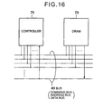
- FIG. 16 is a circuit diagram showing an essential portion of a second example of an electronic apparatus.
- this electronic apparatus includes a DRAM 78, a controller 79 which controls the DRAM 78, and buses 80 such a command bus, an address bus, a data bus and so forth.
- the DRAM 78 is configured to self-manage the refreshment of itself, and, when the time for the refreshment of itself comes, generate the refreshment address internally and start the refreshment of itself, and, when a command is output from the controller 79 while the refreshment of itself being performed, input this command thereto, save the data output from the memory cells to the bit lines during the refreshment of itself in a predetermined internal circuit and interrupt the refreshment of itself, execute the input command, and, then, restart the refreshment of itself after returning the saved data to the bit lines.
- the DRAM 78 is configured to self-manage the refreshment of itself, and, when the time for the refreshment of itself comes, generate the refreshment address internally and perform the refreshment of itself. Therefore, the controller 79 does not need to manage the refreshment of the DRAM 78.
- the DRAM 78 is configured to, when a command is output from the controller 79 during the refreshment of itself, interrupt the refreshment of itself, execute the command output from the controller 79, and, then, restart the refreshment of itself. Accordingly, the controller 78 can access the DRAM 78 without determining whether or not the DRAM 78 is being refreshed.
- FIG. 17 is a circuit diagram showing an essential portion of a second example of a semiconductor memory device.
- This semiconductor memory device can be used as the DRAM 78 shown in FIG. 16 .
- the semiconductor memory device includes a command decoder 82 which decodes command signals from a controller, an address inputting circuit 83 which inputs address signals A0 through An from the controller thereto, and a data inputting/outputting circuit 84 performing inputting/outputting of write data/read data DQ0 through DQn.
- the semiconductor memory device further includes a refreshment control circuit 85 which controls the refreshment of the semiconductor memory device and outputs a refreshment control signal REF periodically, a refreshment counter 86 which uses the refreshment control signal REF as a trigger signal and outputs a refreshment address, and a comparator 87 which compares a row address output from the address inputting circuit 83 with the refreshment address output from the refreshment counter 86.
- a refreshment control circuit 85 which controls the refreshment of the semiconductor memory device and outputs a refreshment control signal REF periodically
- a refreshment counter 86 which uses the refreshment control signal REF as a trigger signal and outputs a refreshment address
- a comparator 87 which compares a row address output from the address inputting circuit 83 with the refreshment address output from the refreshment counter 86.
- the semiconductor memory device further includes banks 88-0 and 88-1 to be selected by a bank address signal.
- the circuit arrangement of the bank 88-0 is the same as that of the bank 88-1.
- the bank 88-0 includes blocks 89-0 through 89-3.
- the blocks 89-0 through 89-3 have the same circuit arrangement.
- the block 89-0 includes a memory cell array 90, a row decoder 91, a sense amplifier 92, and a column decoder 93.
- the block 89-0 further includes a data register 94 for temporarily storing therein data which is being read to the bit lines during the refreshment of the semiconductor memory device, a transfer gate 95 for connecting between the bit lines and the data register 94, and a transfer gate signal generating circuit 96 which controls turning on, off of the transfer gate 95.
- the bank 88-0 further includes a data bus 97 which is used by the block 89-0 through 89-3 in common, write amplifier/sense buffer 98 which is provided for the blocks 89-0 through 89-3 in common, and a control circuit 99 which controls the bank 88-0.
- the bank 88-0 further includes a selector 100 which selects the row address signals output from the address inputting circuit 83 at the time of reading/writing of data, and selects the refreshment address output from the refreshment counter 86 at the time of the refreshment of the semiconductor memory device, and an address latch circuit 101 which holds and outputs the address signals output from the selector 100.
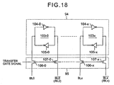
- FIG. 18 is a circuit diagram showing an arrangement of the data register 94 and transfer gate 95.
- bit lines BL0, /BL0, ⁇ ⁇ ⁇ , BLx and /BLx are connected to the transfer gate 95.
- the data register 94 includes flip-flop circuits 103-0, ..., 103-x, which include inverters 104-0, 105-0, ⁇ ⁇ ⁇ , and 104-x and 105-x, respectively.
- the transfer gate 95 includes NMOS transistors 106-0, 107-0, ⁇ ⁇ ⁇ , 106-x and 107-x, turning on, off of each of which is controlled by the transfer gate signal.
- FIGS. 19 and 20 show waveforms for comparing first and second examples of operations of the second example of the semiconductor memory device with an example of operations of a DRAM in the related art.
- FIGS. 19A and 20A show the example of the DRAM in the related art
- FIG. 19B shows the first example of operations of the second example of the semiconductor memory device
- FIG. 20B shows the second example of operations of the second example of the semiconductor memory device.
- the transfer gate signal is caused to have the H level during increase in the voltage between the bit lines BL and /BL by means of the sense amplifier, the transfer gate 95 is turned on, data D0 of the memory cells output to the bit lines BL and /BL is saved in the data register 94, the word line WL0 comes to be non-selected, and, also, the transfer gate signal comes to have the L level, as shown in FIG. 19B .
- the word line WL1 is selected, and read/write operation is performed. Then, when the word line WL1 comes to be non-selected and the read/write operation is finished, the transfer gate signal comes to have the H level, the transfer gate 95 is turned on, the data stored in the data register 94 is transferred to the bit lines BL and /BL, and, also, the word line WL0 is again selected, and the refreshment of the memory cells selected by the word line WL0 is restarted.
- the transfer gate signal is caused to have the H level before the voltage between the bit lines BL and /BL is increased by means of the sense amplifier, that is, at a stage at which the voltage between the bit lines BL and /BL appears by means of the memory cells, the transfer gate 95 is turned on, data D0 of the memory cell output to the bit lines BL and /BL is saved in the data register 94, the transfer gate signal comes to have the L level, and the word line WL0 comes to be non-selected, as shown in FIG. 20B .
- the word line WL1 is selected, and read/write operation is performed. Then, when the word line WL1 comes to be non-selected and the read/write operation is finished, the transfer gate signal comes to have the H level, the transfer gate 95 is turned on, the data stored in the data register 94 is transferred to the bit lines BL and /BL, and, also, the word line WL0 is again selected, the refreshment of the memory cells selected by the word line WL0 is restarted.
- the read/write operation through the word line WL1 is performed at high speed.
- the refreshment of the semiconductor memory device is performed in two steps, that is, a refreshment step 1 and a refreshment step 2.
- the refreshment step 1 the data on the bit lines BL and /BL during the refreshment is saved in the data register 94.
- the refreshment step 2 after execution of a command based on the external access is finished, the data stored in the data register 94 is transferred to the bit lines BL and /BL, and the refreshment is restarted.
- FIG. 21 is a time chart showing a third example of operations of the second example of the semiconductor memory device.
- a plurality of word lines are selected in sequence, and read or write operations are performed on the memory cells selected by these plurality of word lines.
- FIG. 22 shows waveforms illustrating a fourth example of operations of the second example of the semiconductor memory device , and shows a case where no external access occurs during the refreshment of the memory cells through the word line WLO.
- the refreshment is performed wherein the refreshment step 1 and the refreshment step 2 are performed successively. In this case, it is advantageous not to perform turning on of the transfer gate in the refreshment step 2.
- FIGS. 23A and 23B are time charts showing a fifth example of operations and a sixth example of operations of the second example of the semiconductor memory device.
- FIG. 23A shows the fifth example of operations and FIG. 23B shows the sixth example of operations.
- the fifth example of operations of the second example of the semiconductor memory device is an example of operations in a case where access to the word line WL0 is performed by the controller when the word line WL0 is selected for the refreshment of the corresponding memory cells.
- the refreshment step 1 and the refreshment step 2 are performed continuously, and, the second refreshment step 2 is followed by read or write operation on the memory cells selected by the word line WLO.
- the sixth example of operations of the second example of the semiconductor memory device is an example of operations in a case where access to the word line WL1 and access to the word line WL0 are performed by the controller successively when the word line WL0 is selected for the refreshment of the corresponding memory cells.
- read or write operation on the memory cells selected by the word line WL1 is performed after the refreshment step 1 is performed, and, then, continuously, the refreshment step 2 is performed, and, the second refreshment step 2 is followed by read or write operation on the memory cells selected by the word line WLO.
- FIG. 24 shows waveforms illustrating a seventh example of operations of the second example of the semiconductor memory device .
- the time period required for completing data transfer to the data register 94 is determined as a refreshment interruption prohibited period, and the subsequent time period is determined as a refreshment interruption allowed period. Then, a time period for pre-charging required for performing read or write operation after interrupting the refreshment is adjusted depending on the time at which the refreshment has been interrupted.
- the refreshment interruption prohibited period it is possible to interrupt the refreshment at any time (for example, P1, P2, P3) until pre-charging is started after the refreshment interruption prohibited period.
- the time period required for pre-charging after interruption of the refreshment is different depending on the opening width between the bit lines, that is, the time at which the refreshment has been interrupted.
- the time period required for pre-charging becomes longer in the order of the case where the refreshment has been interrupted at P1, the case where the refreshment has been interrupted at P2, the case where the refreshment has been interrupted at P3, and the case where the refreshment has not been interrupted.
- the earlier the refreshment is interrupted the shorter the time period required for pre-charging, by which the refreshment interruption is followed, and the earlier subsequent read or write operation can be started. It is preferable to provide a pre-charging signal generating circuit which enables achievement thereof.
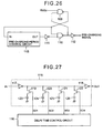
- FIG. 26 is a circuit diagram showing an arrangement of the pre-charging signal generating circuit.
- the pre-charging signal generating circuit includes NAND circuits 109 and 110 which form a flip-flop circuit, inverters 111 and 112, and a pre-charging period control circuit 113 which controls the length of a pre-charging signal, that is, the time period for pre-charging.
- FIG. 27 is a circuit diagram showing an arrangement of the pre-charging period control circuit 113.
- the pre-charging period control circuit 113 includes a variable delaying circuit 115, and a delay time control circuit 116 which outputs delay time control signals SD1 through SD4 for controlling the delay time of the variable delaying circuit 115.
- the delaying circuit 115 includes inverters 117 and 118, NMOS transistors 119 through 122, turning on, off of which is controlled by the delay time control signals SD1 through SD4, and capacitors 123 through 126.
- FIG. 28 is a circuit diagram showing an arrangement of the delay time control circuit 116.
- the delay time control circuit 116 includes a reset signal generating circuit 128 which inputs the RAS activating signal RASz thereto and outputs a reset signal S1, and a refreshment time measuring signal generating circuit 129 which inputs a refreshment interruption prohibiting signal K1 having the H level during the refreshment interruption prohibited period and the internal command signal Com thereto, and generates a refreshment time measuring signal S3.
- the delay time control circuit 116 further includes delaying circuits 130 through 133, which include inverters 134 through 141, and capacitors 142 through 145, respectively.
- the respective delay times of the delaying circuits 130 through 133 are set so that the total of the respective delay times of the delaying circuits 130 through 133 be equal to the refreshment interruption allowed period.
- an inverter 146 inverts the refreshment time measuring signal S3.
- Transfer gates 147 through 150 consist of PMOS transistors and NMOS transistors, respectively. These transfer gates are turned on when the refreshment time measuring signal S3 has the H level and the output of the inverter 146 has the L level. These transfer gates are turned off when the refreshment time measuring signal S3 has the L level and the output of the inverter 146 has the H level.
- latch circuits 151 through 154 hold and output the outputs SD11 through SD14 of the delaying circuits 130 through 133, respectively.
- Inverters 155 through 158 invert the outputs of the latch circuits 151 through 154 and output the delay time control signals SD1 through SD4, respectively.
- PMOS transistors 159 through 162 reset the latch circuits 151 through 154, turning on, off of the transistors 159 through 162 is controlled by the reset signal S1, and the transistors 159 through 162 are turned on when the reset signal S1 has the L level, but are turned off when the reset signal S1 has the H level.
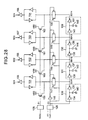
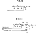
- FIG. 29 is a circuit diagram showing an arrangement of the reset signal generating circuit 128.
- inverters 164 through 166 form a inverting and delaying circuit which inverts and delays the RAS activating signal RASz.
- a NAND circuit 167 processes, in accordance with the NAND manner, the RAS activating signal RASz and the output of the inverter 166, and outputs the reset signal S1.
- FIG. 30 is a circuit diagram showing an arrangement of the refreshment time measuring signal generating circuit 129.
- inverters 170 through 172 form an inverting and delaying circuit which inverts and delays the refreshment interruption prohibiting signal K1.
- a NOR circuit 173 processes, in accordance with the NOR manner, the refreshment interruption prohibiting signal K1 and the output of the inverter 172.
- NOR circuits 174 and 175 form a flip-flop circuit which inputs the output of the NOR circuit 173 and the internal command signal Com thereto.
- An inverter 176 inverts the output of the NOR circuit 174 and outputs the refreshment time measuring signal S3.
- FIGS. 31A through 31J show waveforms illustrating operations of the delay time control circuit 116.
- FIG. 31A shows the RAS activating signal RASz
- FIG. 31B shows the reset signal S1
- FIG. 31C shows the refreshment interruption prohibiting signal K1
- FIG. 31D shows the output S2 of the NOR circuit 173 of the refreshment time measuring signal generating circuit 129
- FIG. 31E shows the internal command signal Com
- FIG. 31F shows the refreshment time measuring signal S3
- FIG. 31G shows the output SD11 of the delaying circuit 130
- FIG. 31H shows the output SD12 of the delaying circuit 131
- FIG. 31I shows the output SD13 of the delaying circuit 132
- FIG. 31J shows the output SD14 of the delaying circuit 133.
- the reset signal S1 having the L level is output from the reset signal generating circuit 128, the PMOS transistors 159 through 162 are turned on, the outputs of the latch circuits 151 through 154 are caused to have the L level, and the delay time control signal SD1 through SD4 are caused to have the H level.
- the refreshment interruption prohibiting signal K1 having the H level is output, the output S2 of the NOR circuit 173 of the refreshment time measuring signal generating circuit 129 comes to have the H level temporarily, and, as a result, the refreshment time measuring signal S3 comes to have the H level. This is delayed by the delaying circuit 130 through 133, and, also, the transfer gates 147 through 150 are turned on.
- the transfer gates 147 through 150 are turned off, and the latch circuits 151 through 154 hold and output the outputs SD11 through SD14 of the delay circuits 130 through 133.
- the outputs of the latch circuits 151 and 152 have the L level
- the outputs of the latch circuits 152 and 153 have the H level
- the delay time control signals SD1 and SD2 have the H level
- the delay time control signals SD3 and SD4 have the L level.
- the thus obtained delay time is such as that obtained only by means of the capacitors 123 and 124. That is, in the second example of the semiconductor memory device, the time for pre-charging is set depending on the length of the refreshment time measuring signal S3, that is, the time period during which the refreshment time measuring signal S3 has the H level.
- the pre-charging signal is generated for a time period depending on a time period of the refreshment.
- the pre-charging signal is generated for the time period equal to the delay time obtained by means of the capacitor 123.
- the pre-charging signal is generated for the time period equal to the delay time obtained by means of the capacitors 123 and 124.
- the pre-charging signal is generated for the time period equal to the delay time obtained by means of the capacitors 123 through 125.
- the pre-charging signal is generated for the time period equal to the delay time obtained by means of the capacitors 123 through 126.
- FIGS. 32A through 32K show waveforms illustrating an example operations of the second example of the semiconductor memory device .
- FIG. 32A shows the RAS activating signal RASz
- FIG. 32B shows a refreshment timing signal
- FIG. 32C shows the transfer gate signal
- FIG. 32D shows the refreshment interruption prohibiting signal K1
- FIG. 32E shows the internal command signal Com
- FIG. 32F shows the refreshment time measuring signal S3
- FIG. 32G shows a write back flag signal
- FIG. 32H shows the pre-charging signal
- FIG. 32I shows a write back start signal
- FIG. 32J shows a write back end measuring signal
- FIG. 32K shows a write back end signal.
- a refreshment timing signal is generated.
- the RAS activating signal RASz is generated.
- the transfer gate signal for transferring the data on the bit lines during the refreshment to the data register 94 and the refreshment interruption prohibiting signal K1 for setting the refreshment interruption prohibited period are generated.
- the refreshment interruption prohibiting signal K1 is negated. Then, after that, when a command is input, in response thereto, the refreshment is interrupted. When a command is input during the refreshment interruption prohibited period, the refreshment is interrupted immediately after the refreshment interruption prohibiting signal K1 is negated.
- the refreshment time measuring signal S3 for measuring the time period from the time the refreshment interruption prohibiting signal K1 is negated to the time the command is input is generated, and, depending on the length of the refreshment time measuring signal S3 (time period during which the refreshment time measuring signal S3 has the H level), the pre-charging time is set.
- the write back flag signal when the refreshment is interrupted and a command is executed, the write back flag signal is generated in response to the interruption of the refreshment.
- the write back flag signal expresses necessity of writing back of the data from the data register 94 to the bit lines, which should be performed in the refreshment step 2 after the command is executed.
- the write back flag signal is output, and, also, execution of the command is finished (the internal command signal Com come to have the L level)
- a write back start signal is caused to have the H level.
- the write back start signal is caused to have the L level.
- the RAS activating signal is caused to have the H level for the writing back operation, and, also, a write back end measuring signal is caused to have the H level.
- the level of the write back end measuring signal returns from the H level to the L level when the time required for the writing back operation has elapsed.
- the write back end signal is a signal having a pulse of the H level when the RAS activating signal RASz comes to have the L level after the write back end measuring signal comes to have the L level, and indicating that the writing back operation has been finished, but maintaining to have the L level when the RAS activating signal RASz comes to have the L level before the write back end measuring signal comes to have the L level (when a command is input during the writing back operation), and indicating that the writing back operation has not been finished. Accordingly, when a command is input during the writing back operation, the writing back operation is interrupted, and, after execution of the command is performed, the writing back operation is performed.
- the refreshment control circuit 85 manages the refreshment of the semiconductor memory device, and, when the time for the refreshment of the semiconductor memory device comes and there is no command which is being processed, the refreshment of the semiconductor memory device can be performed based on the refreshment address output from the refreshment counter 86 immediately.
- the refreshment of the semiconductor memory device can be performed based on the refreshment address output from the refreshment counter 86 after the command is executed. Accordingly, the controller does not need to manage the refreshment of the semiconductor memory device.
- command signals can be accepted by the second example of the semiconductor memory device even during refreshment of the semiconductor memory device.
- the refreshment is interrupted and the command is executed. Then, the refreshment can be restarted. Accordingly, the controller can access the second example of the semiconductor memory device without monitoring whether or not this semiconductor memory device is being refreshed. As a result, it is possible to perform efficient operations.
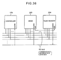
- FIG. 33 is a circuit diagram showing an essential portion of a third example of an electronic apparatus.
- a controller 179 controls a DRAM 178, and a flash memory 180 is used for saving therein data stored in the DRAM 178.
- This electronic apparatus further includes buses 181 such as a command bus, an address bus, a data bus and so forth.
- the flash memory 180 is configured to output a busy signal BUSY2 during read/write/erase operation, that it, when not able to accept access thereto.
- the controller 179 is configured to cause all command signals and address signals to have the L level when a main battery goes dead, or is removed, and, thereby, power supply by the main battery is stopped.
- the DRAM 178 is configured to automatically output the data to the data bus in accordance with the addresses generated by an internal address counter for saving the data, when the busy signal BUSY2 is not output from the flash memory 180 in a case where all the command signals and address signals output from the controller 179 have the L level.
- the flash memory 180 is configured to automatically write thereto the data output from the DRAM 178 based on the addresses generated by an internal address counter in a case where all the command signals and address signals output from the controller 179 have the L level.
- the data stored in the DRAM 178 is saved in the flash memory 180 which does not need to be refreshed, when the main battery goes dead, or is removed, and, thereby, power supply by the main battery is stopped.
- the third example of the electronic apparatus when the third example of the electronic apparatus is applied to a simple terminal such as a cellular phone in which a DRAM is mounted, power consumption of a backup battery due to the refreshment of the DRAM 178 can be reduced as much as possible, when a main battery goes dead, or is removed, and, thereby, power supply by the main battery is stopped.
- the flash memory 180 is configured to output the busy signal BUSY2 during read/write/erase operation
- the DRAM 178 is configured to perform the refreshment thereof using a time during which the busy signal BUSY2 is output, the refreshment of the DRAM 178 can be performed while the data is being saved in the flash memory 180 and necessary data can be retained by the DRAM 178.
- the flash memory 180 which is a nonvolatile semiconductor memory device is provided for saving therein the data stored in the DRAM 178.
- various semiconductor memory devices which do not need to be refreshed can be used.
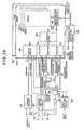
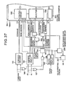
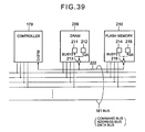
- FIG. 34 is a circuit diagram showing an essential portion of a third example of a semiconductor memory device .
- This semiconductor memory device can be used as the DRAM 178 included in the third example of the electronic apparatus shown in FIG. 33 .
- a command decoder 183 decodes command signals from the controller 179, an address inputting circuit 184 inputs thereto address signals A0 through An, and a data inputting/outputting circuit 185 performs inputting/outputting of read/write data DQO through DQn.
- NOR circuit 186 processes, in accordance with the NOR manner, the command signals from the controller 179
- NOR circuit 187 processes, in accordance with the NOR manner, the address signals A0 through An
- NAND circuit 188 processes, in accordance with the NAND manner, the respective outputs of the NOR circuits 186 and 187.
- the output of the NOR circuit 186 has the H level only when all the command signals have the L level, and the output of the NOR circuit 187 has the H level only when all the address signals A0 through An have the L level. Therefore, the output of the NAND circuit 188 has the L level only when all the command signals and address signals A0 through An have the L level. In this case, this semiconductor memory device automatically enters a data saving mode.
- a BUSY2 inputting buffer 189 is used for receiving the busy signal BUSY2 from the flash memory 180, a data saving control circuit 190 controls saving of data.
- the data saving control circuit 190 outputs a busy enable signal BEN for activating the BUSY2 inputting buffer 189, and, also, outputs a data saving control signal ESC, when the output of the NAND circuit 188 has the L level, that is, when all the command signals and address signals A0 through An from the controller 179 have the L level. Then, the data saving control circuit 190 outputs the data saving control signal ESC each time the BUSY2 inputting buffer 189 inputs the busy signal BUSY2 thereto.
- a data saving address counter 191 receives the data saving control signal ESC and outputs the addresses from which the data to be saved is read
- a refreshment control circuit 192 receives the data saving control signal ESC and outputs a refreshment control signal REF
- a refreshment counter 193 uses the refreshment control signal REF as a trigger signal and outputs the refreshment addresses.
- banks 194-0 and 194-1 are selected by a bank address signal.
- the banks 194-0 and 194-1 have the same circuit arrangement.
- blocks 195-0 through 195-3 have the arrangements same as those of the blocks 12-0 through 12-3 shown in FIG. 3 .
- a bus 196 is provided for the blocks 195-0 through 195-3 in common
- a write amplifier/sense buffer 197 is provided for the blocks 195-0 through 195-3 in common
- a control circuit 198 controls the operation of the bank 194-0.
- a selector 199 is controlled by the control circuit 198 and selects the row address output from the address inputting circuit 184 when read/write operation is performed in the semiconductor memory device, selects the refreshment address output from the refreshment counter 193 when the refreshment of the semiconductor memory device is performed, selects the data saving address output from the data saving address counter 191 when the data is saved in the flash memory 180.
- An address latch circuit 200 holds and outputs the address signals output from the selector 199.
- a column address counter 201 is also provided.
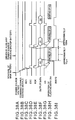
- FIGS. 35A through 35G show waveforms illustrating an example of operations in a case where the third example of the semiconductor memory device is applied to the DRAM 178 of the electronic apparatus shown in FIG. 33 .
- FIG. 35A shows a power supply voltage supplied by the main battery
- FIG. 35B shows command signals and address signals output from the controller
- FIG. 35C shows the busy enable signal BEN
- FIG. 35D shows the data saving signal ESC
- FIG. 35E shows output data
- FIG. 35F shows the operation state of the flash memory 180
- FIG. 35G shows the busy signal BUSY2.
- the busy signal BUSY2 comes to have the H level and is provided to the data saving control circuit 190 via the BUSY inputting circuit 189. Then, the second data saving control signal ESC is output. In response thereto, the second data D1 to be saved is output, and is written to the flash memory 180. During this time, the busy signal BUSY2 comes to have the L level, and indicates that the data is being written to the flash memory 180. During the time during which the busy signal BUSY2 has the L level, the data saving control signal ESC is stopped, and the refreshment of this semiconductor memory device is restarted.
- the busy signal BUSY2 comes to have the H level and is provided to the data saving control circuit 190 via the BUSY inputting circuit 189. Then, the third data saving control signal ESC is output. In response thereto, the third data D2 to be saved is output, and is written to the flash memory 180. During this time, the busy signal BUSY2 comes to have the L level, and indicates that the data is being written to the flash memory 180. Then, the same operations are repeated until all the data to be saved is output and written to the flash memory 180.
- the third example of the semiconductor memory device when the third example of the semiconductor memory device is applied to a simple terminal such as a cellular phone in which a DRAM is mounted, power consumption of a backup battery due to the refreshment of the DRAM 178 can be reduced as much as possible, when a main battery goes dead, or is removed, and, thereby, power supply by the main battery is stopped.
- FIG. 36 is a circuit diagram showing an essential portion of a fourth example of an electronic apparatus .
- the fourth example of the electronic apparatus is provide with a DRAM 203 and a flash memory 204 having circuit arrangements different from the DRAM 178 and flash memory 180 which the third example of the electronic apparatus shown in FIG. 33 is provided with. Except therefor, the fourth example of the electronic apparatus has the same arrangement as that of the third example of the electronic apparatus shown in FIG. 33 .
- the DRAM-203 is configured to output data and also a data strobe signal QS which indicates timing in which the output data is to be brought in.
- the flash memory204 is configured to receives the data strobe signal QS from the DRAM 203, and can bring therein the output data from the DRAM 203 in the timing indicated by the data strobe signal QS.
- FIG. 37 is a circuit diagram showing an essential portion of a fourth example of a semiconductor memory device .
- the fourth example of the semiconductor memory device can be used as the DRAM 203 which the fourth example of the electronic apparatus shown in FIG. 36 is provided with.
- the fourth example of the semiconductor memory device is provided with a data saving clock signal generating circuit 206 which generates a data saving clock signal (clock signal for the data saving operation) and a QS outputting circuit 207 which generates the data strobe signal QS.
- the data saving clock signal is output from the data saving clock signal generating circuit 206, then, the data saving address counter 191, QS outputting circuit 207 and so forth are operated in synchronization with the data saving clock signal, so that the output timing of the data strobe signal QS and the output data becomes the proper one.
- the fourth example of the semiconductor memory device has the same arrangement as that of the third example of the semiconductor memory device shown in FIG. 34 .
- the data saving clock signal generating circuit 206 may have an oscillator built therein for generating the data saving clock signal.
- the data saving clock signal generating circuit 206 may use a clock signal from a crystal oscillator or the like which an electronic apparatus using the fourth example- of the semiconductor memory device provided with for generating the data saving clock signal.
- FIGS. 38A through 38I show waveforms illustrating an example of operations in a case where the fourth example of the semiconductor memory device is applied to the DRAM 203 of the electronic apparatus shown in FIG. 36 .
- FIG. 38A shows a power supply voltage supplied by the main battery
- FIG. 38B shows command signals and address signals output from the controller
- FIG. 38C shows the busy enable signal BEN
- FIG. 38D shows the data saving signal ESC
- FIG. 38E shows the data saving clock signal ECK output from the data saving clock signal generating circuit 206
- FIG. 35F shows output data
- FIG. 35G shows the data strobe signal QS
- FIG. 35H shows the operation state of the flash memory 204
- FIG. 35I shows the busy signal BUSY2.
- the busy signal BUSY2 comes to have the L level, and indicates that data is being written to the flash memory 204.
- the data saving control signal ESC is stopped, and the refreshment of this semiconductor memory device is restarted.
- the busy signal BUSY2 comes to have the H level and is provided to the data saving control circuit 190 via the BUSY inputting circuit 189. Then, the second data saving control signal ESC is output. In response thereto, the second data D1 to be saved is output, and, also the data strobe signal QS is output. Then, the data D1 is written to the flash memory 204.
- the busy signal BUSY2 comes to have the L level, and indicates that the data is being written to the flash memory 204.
- the data saving control signal ESC is stopped, and the refreshment of this semiconductor memory device is restarted.
- the busy signal BUSY2 comes to have the H level and is provided to the data saving control circuit 190 via the BUSY inputting circuit 189. Then, the third data saving control signal ESC is output. In response thereto, the third data D2 to be saved is output, and, also the data strobe signal QS is output. Then, the data D2, and is written to the flash memory 204. During this time, the busy signal BUSY2 comes to have the L level, and indicates that the data is being written to the flash memory 204. Then, the same operations are repeated until all the data to be saved is output and written to the flash memory 204.
- FIG. 39 is a circuit diagram showing an essential portion of a fifth example of an electronic apparatus
- the fifth example of the electronic apparatus is provided with a DRAM 209 and a flash memory 210 having circuit arrangements different from the DRAM 178 and flash memory 180 which the third example of the electronic apparatus shown in FIG. 33 is provided with. Except therefor, the fifth example of the electronic apparatus has the same arrangement as that of the third example of the electronic apparatus shown in FIG. 33 .
- the DRAM 209 has a BUSY2 inputting circuit 211 for inputting the busy signal BUSY2 and a QS outputting circuit 212 for outputting the data strobe signal QS built therein, and is provided with an external terminal 213 which is used both as a busy signal inputting terminal and as a data strobe signal outputting terminal.
- the flash memory 210 has a BUSY2 outputting circuit 214 for outputting the busy signal BUSY2 and a QS inputting circuit 215 for inputting the data strobe signal QS built therein, and is provided with an external terminal 216 which is used both as a busy signal outputting terminal and as a data strobe signal inputting terminal.
- FIG. 40 is a circuit diagram showing an example of arrangements of the BUSY2 inputting circuit 211, QS outputting circuit 212, BUSY2 outputting circuit 214 and QS inputting circuit 215.
- an inverter 218 is used for inputting the busy signal BUSY2
- an NMOS transistor 219 is used for outputting the data strobe signal QS.
- an NMOS transistor 220 is used for outputting the busy signal BUSY2, and, in the QS inputting circuit 215, an inverter 221 is used for inputting the data strobe signal QS.
- a high-resistance resistor 223 is needed to be provided between the BUSY2/QS common line 222 and the power-source voltage line VDD, in order to keep the signal levels of the busy signal BUSY2 and data strobe signal QS in the proper levels, respectively.
- FIG. 41 is a circuit diagram showing an essential portion of a fifth example of a semiconductor memory device .
- the fifth example of the semiconductor memory device can be used as the DRAM 209 which the fifth example of the electronic apparatus shown in FIG. 39 is provided with.
- the fifth example of the semiconductor memory device is provided with an external terminal 225 which is used both as a busy signal inputting terminal and as a data strobe signal outputting terminal.
- the external terminal 225 is connected with the input terminal 226 of the BUSY2 inputting circuit 189 and with the output terminal of the QS outputting circuit 207. Except therefor, the fifth example of the semiconductor memory device has the same arrangement as that of the fourth example - of the semiconductor memory device shown in FIG 37 .
- FIGS. 42A through 42G show waveforms illustrating an example of operations in a case where the fifth example - of the semiconductor memory device is applied to the DRAM 209 of the electronic apparatus shown in FIG. 39 .
- FIG. 42A shows a power supply voltage supplied by a main battery
- FIG. 42B shows the state of command signals and address signals output from the controller
- FIG. 42C shows the busy enable signal BEN
- FIG. 42D shows the data saving signal ESC
- FIG. 42E shows output data
- FIG. 42F shows the electric potential of the BUSY2/QS common line
- FIG. 42G shows the state of the flash memory 210.
- the first data D0 to be saved is output from the semiconductor memory device, also the data strobe signal QS having the L level is output to the BUSY2/QS common line, the data D0 to be saved is brought in by the flash memory 210 in synchronization with the data strobe signal QS and is written to the flash memory 210.
- the busy signal BUSY2 having the L level is output to the BUSY2/QS common line, and, thus, it is indicated that data is being written to the flash memory 210.
- the signal on the BUSY2/QS common line comes to have the H level, and is provided to the data saving control circuit 190 via the BUSY inputting circuit 189.
- the second data saving control signal ESC is output.
- the second data D1 to be saved is output from the semiconductor memory device, also the data strobe signal QS having the L level is output to the BUSY2/QS common line, the data D1 to be saved is brought in by the flash memory 210 in synchronization with the data strobe signal QS and is written to the flash memory 210.
- the busy signal BUSY2 having the L level is output to the BUSY2/QS common line, and, thus, it is indicated that data is being written to the flash memory 210.
- the signal on the BUSY2/QS common line comes to have the H level, and is provided to the data saving control circuit 190 via the BUSY inputting circuit 189.
- the third data saving control signal ESC is output.
- the third data D2 to be saved is output from the semiconductor memory device, also the data strobe signal QS having the L level is output to the BUSY2/QS common line, the data D2 to be saved is brought in by the flash memory 210 in synchronization with the data strobe signal QS and is written to the flash memory 210.
- the busy signal BUSY2 having the L level is output to the BUSY2/QS common line, and, thus, it is indicated that data is being written to the flash memory 210.
- FIGS. 43A through 43H data to be saved consisting of a plurality of bytes may be output all together in a burst mode.
- FIG. 43A shows the power supply voltage supplied by the main battery
- FIG. 43B shows the state of command signals and address signals output from the controller
- FIG. 43C shows the busy enable signal BEN
- FIG. 43D shows the data saving signal ESC
- FIG. 43E shows output data
- FIG. 43F shows the data strobe signal QS
- FIG. 43G shows the state of the flash memory 210
- FIG. 43H shows the busy signal BUSY2.
- FIG. 44 is a circuit diagram showing an essential portion of a sixth example of a semiconductor memory device .
- This semiconductor memory device can be used as the DRAM 203 shown in FIG. 36 .
- the sixth example of the semiconductor memory device is provided with a comparator 229 which compares the data saving address output from the data saving address counter 191 with the refreshment address output from the refreshment counter 193, and an AND circuit 230 which uses the output N2 of the comparator 229 as a gate signal therefor and controls transmission of the refreshment control signal REF output from the refreshment control circuit 192. Except therefor, this semiconductor memory device has the same arrangement as that of the fourth example of the semiconductor memory device shown in FIG. 37 .
- the comparator 229 is controlled by a control signal N1 output from the data saving control circuit 190 and performs the comparison operation when the control signal N1 has the H level.
- the control signal N1 has the H level in the data saving mode, but has the L level in all the other cases.
- the output N2 of the comparator 229 has -the H level only when the refreshment address is larger than the data saving address, but has the L level in all the other cases.
- the refreshment control signal REF is output. Thereby, the refreshment is performed for the output refreshment address.
- the refreshment control signal REF is not output from the AND circuit 230. Thereby, the refreshment is not performed for the output refreshment address.
- the same advantages as those obtained from the fourth example of the semiconductor memory device shown in FIG. 37 can be obtained. Also, for the addresses, the data at which have been already saved, the refreshment is not performed. As a result, it is possible to reduce power consumption of a backup battery to an amount smaller than that in the case of the fourth example of the semiconductor memory device shown in FIG. 37 .
- FIG. 45 is a circuit diagram showing an essential portion of a seventh example of a semiconductor memory device .
- This semiconductor memory device is provided with banks 232-0 and 232-1 having circuit arrangements different from those of the banks 194-0 and 194-1 which the third example of the semiconductor memory device shown in FIG. 34 is provided with. Except therefor, the seventh example - of the semiconductor memory device has the same arrangement as that of the third example of the semiconductor memory device according to the present invention shown in FIG. 34 .
- the banks 232-0 and 232-1 have the same circuit arrangement.
- blocks 233-0 through 233-3 are provided.
- the blocks 233-0 through 233-3 have the same circuit arrangement.
- a memory cell array 234, a row decoder 235, a sense amplifier 236, a column decoder 237, and a transfer gate 238 are provided.
- the transfer gate 238 is connected with a control circuit 239 and is used for transferring data read from the memory cell array 234 to a serial register which will be described later when the data stored in this semiconductor memory device is saved in a flash memory or the like.
- serial register 240 is provided for the blocks 233-0 through 233-3 in common, and a write amplifier/sense buffer 241 is provided for the blocks 233-0 through 233-3 in common.
- the sense buffer operates so as to provide data output from the serial register 240 to the data inputting/outputting circuit 185 when the data stored in this semiconductor memory device is saved in the flash memory or the like.
- the other portions of the banks 232-0 and 232-1 have the same arrangements as those of the banks 194-0 and 194-1 shown in FIG. 34 .
- data to be saved is stored in the serial register 240 for each row, and the data to be saved thus stored in the serial register is output from this semiconductor memory device via the sense buffer and data inputting/outputting circuit 185.
- the refreshment operation can be performed while data is being output to be saved. Accordingly, it is possible to achieve high-efficiency operations.
Landscapes
- Engineering & Computer Science (AREA)
- Microelectronics & Electronic Packaging (AREA)
- Computer Hardware Design (AREA)
- Databases & Information Systems (AREA)
- Dram (AREA)
- Memory System (AREA)
Applications Claiming Priority (2)
| Application Number | Priority Date | Filing Date | Title |
|---|---|---|---|
| JP16346199 | 1999-06-10 | ||
| JP16346199A JP4106811B2 (ja) | 1999-06-10 | 1999-06-10 | 半導体記憶装置及び電子装置 |
Publications (2)
| Publication Number | Publication Date |
|---|---|
| EP1061523A1 EP1061523A1 (en) | 2000-12-20 |
| EP1061523B1 true EP1061523B1 (en) | 2009-11-18 |
Family
ID=15774329
Family Applications (1)
| Application Number | Title | Priority Date | Filing Date |
|---|---|---|---|
| EP00302717A Expired - Lifetime EP1061523B1 (en) | 1999-06-10 | 2000-03-31 | Semiconductor memory device and electronic apparatus |
Country Status (6)
| Country | Link |
|---|---|
| US (2) | US6535950B1 (ja) |
| EP (1) | EP1061523B1 (ja) |
| JP (1) | JP4106811B2 (ja) |
| KR (2) | KR100607918B1 (ja) |
| DE (1) | DE60043326D1 (ja) |
| TW (1) | TW468184B (ja) |
Families Citing this family (56)
| Publication number | Priority date | Publication date | Assignee | Title |
|---|---|---|---|---|
| JP3624849B2 (ja) | 2001-04-02 | 2005-03-02 | セイコーエプソン株式会社 | 半導体装置、そのリフレッシュ方法、メモリシステムおよび電子機器 |
| JP4712214B2 (ja) * | 2001-04-09 | 2011-06-29 | 富士通セミコンダクター株式会社 | 半導体メモリの動作制御方法および半導体メモリ |
| JP2003228511A (ja) * | 2002-02-04 | 2003-08-15 | Elpida Memory Inc | データ書込方法及びメモリシステム |
| US7043599B1 (en) | 2002-06-20 | 2006-05-09 | Rambus Inc. | Dynamic memory supporting simultaneous refresh and data-access transactions |
| KR100455393B1 (ko) * | 2002-08-12 | 2004-11-06 | 삼성전자주식회사 | 리프레시 플래그를 발생시키는 반도체 메모리 장치 및반도체 메모리 시스템. |
| EP1542237A4 (en) * | 2002-09-20 | 2008-08-06 | Fujitsu Ltd | SEMICONDUCTOR MEMORY |
| JP4996094B2 (ja) * | 2003-10-24 | 2012-08-08 | インターナショナル・ビジネス・マシーンズ・コーポレーション | 半導体記憶装置及びそのリフレッシュ方法 |
| KR20060009446A (ko) * | 2004-07-22 | 2006-02-01 | 삼성전자주식회사 | 프로세서의 오동작을 방지할 수 있는 정보 처리 장치 |
| JP4562468B2 (ja) * | 2004-09-13 | 2010-10-13 | ルネサスエレクトロニクス株式会社 | 半導体記憶装置 |
| KR100574989B1 (ko) * | 2004-11-04 | 2006-05-02 | 삼성전자주식회사 | 데이터 스트로브 버스라인의 효율을 향상시키는메모리장치 및 이를 구비하는 메모리 시스템, 및 데이터스트로브 신호 제어방법 |
| WO2006080065A1 (ja) | 2005-01-27 | 2006-08-03 | Spansion Llc | 記憶装置、およびその制御方法 |
| JP4756581B2 (ja) * | 2005-07-21 | 2011-08-24 | ルネサスエレクトロニクス株式会社 | 半導体記憶装置 |
| WO2007032996A2 (en) * | 2005-09-07 | 2007-03-22 | Ace*Comm Corporation | Consumer configurable mobile communication solution |
| JP2007115087A (ja) * | 2005-10-21 | 2007-05-10 | Oki Electric Ind Co Ltd | 半導体装置 |
| CN101689130A (zh) | 2006-12-06 | 2010-03-31 | 弗森多系统公司(dba弗森-艾奥) | 采用渐进raid存储数据的装置、系统和方法 |
| US7797511B2 (en) * | 2007-01-05 | 2010-09-14 | Qimonda North America Corp. | Memory refresh system and method |
| US8767450B2 (en) * | 2007-08-21 | 2014-07-01 | Samsung Electronics Co., Ltd. | Memory controllers to refresh memory sectors in response to writing signals and memory systems including the same |
| KR20100134375A (ko) * | 2009-06-15 | 2010-12-23 | 삼성전자주식회사 | 리프레쉬 동작을 수행하는 메모리 시스템 |
| US7836226B2 (en) | 2007-12-06 | 2010-11-16 | Fusion-Io, Inc. | Apparatus, system, and method for coordinating storage requests in a multi-processor/multi-thread environment |
| US8064250B2 (en) * | 2008-12-16 | 2011-11-22 | Micron Technology, Inc. | Providing a ready-busy signal from a non-volatile memory device to a memory controller |
| DE112008000968T5 (de) * | 2008-12-30 | 2012-01-12 | Numonyx B.V. | Nicht-flüchtiger Speicher mit erweitertem Betriebstemperaturbereich |
| US9021158B2 (en) | 2009-09-09 | 2015-04-28 | SanDisk Technologies, Inc. | Program suspend/resume for memory |
| US9223514B2 (en) | 2009-09-09 | 2015-12-29 | SanDisk Technologies, Inc. | Erase suspend/resume for memory |
| US8972627B2 (en) * | 2009-09-09 | 2015-03-03 | Fusion-Io, Inc. | Apparatus, system, and method for managing operations for data storage media |
| CN102597910B (zh) | 2009-09-09 | 2015-03-25 | 弗森-艾奥公司 | 存储设备中用于功率减小管理的装置、系统及方法 |
| US8984216B2 (en) | 2010-09-09 | 2015-03-17 | Fusion-Io, Llc | Apparatus, system, and method for managing lifetime of a storage device |
| US10817502B2 (en) | 2010-12-13 | 2020-10-27 | Sandisk Technologies Llc | Persistent memory management |
| US9208071B2 (en) | 2010-12-13 | 2015-12-08 | SanDisk Technologies, Inc. | Apparatus, system, and method for accessing memory |
| US9218278B2 (en) | 2010-12-13 | 2015-12-22 | SanDisk Technologies, Inc. | Auto-commit memory |
| US10817421B2 (en) | 2010-12-13 | 2020-10-27 | Sandisk Technologies Llc | Persistent data structures |
| US9911485B2 (en) * | 2013-11-11 | 2018-03-06 | Qualcomm Incorporated | Method and apparatus for refreshing a memory cell |
| US9666244B2 (en) | 2014-03-01 | 2017-05-30 | Fusion-Io, Inc. | Dividing a storage procedure |
| KR20160063726A (ko) * | 2014-11-27 | 2016-06-07 | 에스케이하이닉스 주식회사 | 메모리 장치 및 이를 포함하는 메모리 시스템 |
| US9933950B2 (en) | 2015-01-16 | 2018-04-03 | Sandisk Technologies Llc | Storage operation interrupt |
| KR102384962B1 (ko) * | 2015-11-27 | 2022-04-11 | 에스케이하이닉스 주식회사 | 반도체 메모리 장치 |
| DE102017106713A1 (de) * | 2016-04-20 | 2017-10-26 | Samsung Electronics Co., Ltd. | Rechensystem, nichtflüchtiges Speichermodul und Verfahren zum Betreiben einer Speichervorrichtung |
| US10490251B2 (en) | 2017-01-30 | 2019-11-26 | Micron Technology, Inc. | Apparatuses and methods for distributing row hammer refresh events across a memory device |
| WO2019222960A1 (en) | 2018-05-24 | 2019-11-28 | Micron Technology, Inc. | Apparatuses and methods for pure-time, self adopt sampling for row hammer refresh sampling |
| US10685696B2 (en) | 2018-10-31 | 2020-06-16 | Micron Technology, Inc. | Apparatuses and methods for access based refresh timing |
| WO2020117686A1 (en) | 2018-12-03 | 2020-06-11 | Micron Technology, Inc. | Semiconductor device performing row hammer refresh operation |
| CN111354393B (zh) | 2018-12-21 | 2023-10-20 | 美光科技公司 | 用于目标刷新操作的时序交错的设备和方法 |
| JP6894459B2 (ja) * | 2019-02-25 | 2021-06-30 | 華邦電子股▲ふん▼有限公司Winbond Electronics Corp. | 疑似スタティックランダムアクセスメモリとその動作方法 |
| US11615831B2 (en) | 2019-02-26 | 2023-03-28 | Micron Technology, Inc. | Apparatuses and methods for memory mat refresh sequencing |
| US11227649B2 (en) | 2019-04-04 | 2022-01-18 | Micron Technology, Inc. | Apparatuses and methods for staggered timing of targeted refresh operations |
| US11069393B2 (en) | 2019-06-04 | 2021-07-20 | Micron Technology, Inc. | Apparatuses and methods for controlling steal rates |
| US10978132B2 (en) | 2019-06-05 | 2021-04-13 | Micron Technology, Inc. | Apparatuses and methods for staggered timing of skipped refresh operations |
| US11302374B2 (en) | 2019-08-23 | 2022-04-12 | Micron Technology, Inc. | Apparatuses and methods for dynamic refresh allocation |
| US11302377B2 (en) | 2019-10-16 | 2022-04-12 | Micron Technology, Inc. | Apparatuses and methods for dynamic targeted refresh steals |
| US11309010B2 (en) * | 2020-08-14 | 2022-04-19 | Micron Technology, Inc. | Apparatuses, systems, and methods for memory directed access pause |
| US11380382B2 (en) | 2020-08-19 | 2022-07-05 | Micron Technology, Inc. | Refresh logic circuit layout having aggressor detector circuit sampling circuit and row hammer refresh control circuit |
| US11348631B2 (en) | 2020-08-19 | 2022-05-31 | Micron Technology, Inc. | Apparatuses, systems, and methods for identifying victim rows in a memory device which cannot be simultaneously refreshed |
| US11430504B2 (en) * | 2020-08-27 | 2022-08-30 | Micron Technology, Inc. | Row clear features for memory devices and associated methods and systems |
| US11557331B2 (en) | 2020-09-23 | 2023-01-17 | Micron Technology, Inc. | Apparatuses and methods for controlling refresh operations |
| US11222686B1 (en) | 2020-11-12 | 2022-01-11 | Micron Technology, Inc. | Apparatuses and methods for controlling refresh timing |
| US11264079B1 (en) | 2020-12-18 | 2022-03-01 | Micron Technology, Inc. | Apparatuses and methods for row hammer based cache lockdown |
| US11972788B2 (en) * | 2021-03-11 | 2024-04-30 | Micron Technology, Inc. | Apparatuses, systems, and methods for controller directed targeted refresh operations based on sampling command |
Family Cites Families (23)
| Publication number | Priority date | Publication date | Assignee | Title |
|---|---|---|---|---|
| US4145739A (en) * | 1977-06-20 | 1979-03-20 | Wang Laboratories, Inc. | Distributed data processing system |
| JPS6079593A (ja) | 1983-10-07 | 1985-05-07 | Hitachi Ltd | 半導体集積回路システム |
| US4639890A (en) * | 1983-12-30 | 1987-01-27 | Texas Instruments Incorporated | Video display system using memory with parallel and serial access employing selectable cascaded serial shift registers |
| US4758993A (en) | 1984-11-19 | 1988-07-19 | Fujitsu Limited | Random access memory device formed on a semiconductor substrate having an array of memory cells divided into sub-arrays |
| US4829467A (en) | 1984-12-21 | 1989-05-09 | Canon Kabushiki Kaisha | Memory controller including a priority order determination circuit |
| US4691303A (en) | 1985-10-31 | 1987-09-01 | Sperry Corporation | Refresh system for multi-bank semiconductor memory |
| JPH07107793B2 (ja) | 1987-11-10 | 1995-11-15 | 株式会社東芝 | 仮想型スタティック半導体記憶装置及びこの記憶装置を用いたシステム |
| FR2644260B1 (fr) | 1989-03-08 | 1993-10-29 | Nec Corp | Dispositif de commande d'acces en memoire pouvant proceder a une commande simple |
| JP2827361B2 (ja) | 1989-12-04 | 1998-11-25 | 日本電気株式会社 | 半導体メモリ装置 |
| DE4118804C2 (de) * | 1990-06-08 | 1996-01-04 | Toshiba Kawasaki Kk | Serienzugriff-Speicheranordnung |
| EP0552667B1 (en) * | 1992-01-22 | 1999-04-21 | Enhanced Memory Systems, Inc. | Enhanced dram with embedded registers |
| GB2265035B (en) | 1992-03-12 | 1995-11-22 | Apple Computer | Method and apparatus for improved dram refresh operations |
| US5519839A (en) | 1992-10-02 | 1996-05-21 | Compaq Computer Corp. | Double buffering operations between the memory bus and the expansion bus of a computer system |
| US5617367A (en) * | 1993-09-01 | 1997-04-01 | Micron Technology, Inc. | Controlling synchronous serial access to a multiport memory |
| KR970008412B1 (ko) * | 1993-10-15 | 1997-05-23 | 엘지반도체 주식회사 | 디지탈 영상신호 처리용 메모리 시스템 |
| KR0171930B1 (ko) * | 1993-12-15 | 1999-03-30 | 모리시다 요이치 | 반도체 메모리, 동화기억 메모리, 동화기억장치, 동화표시장치, 정지화기억 메모리 및 전자노트 |
| US5634073A (en) | 1994-10-14 | 1997-05-27 | Compaq Computer Corporation | System having a plurality of posting queues associated with different types of write operations for selectively checking one queue based upon type of read operation |
| JPH08129882A (ja) | 1994-10-31 | 1996-05-21 | Mitsubishi Electric Corp | 半導体記憶装置 |
| US5796671A (en) * | 1996-03-01 | 1998-08-18 | Wahlstrom; Sven E. | Dynamic random access memory |
| FR2749681B1 (fr) | 1996-06-10 | 1998-07-10 | Bull Sa | Circuit pour transborder des donnees entre memoires distantes et calculateur comprenant un tel circuit |
| JPH10247384A (ja) | 1997-03-03 | 1998-09-14 | Mitsubishi Electric Corp | 同期型半導体記憶装置 |
| US6396744B1 (en) * | 2000-04-25 | 2002-05-28 | Multi Level Memory Technology | Flash memory with dynamic refresh |
| US6515914B2 (en) * | 2001-03-21 | 2003-02-04 | Micron Technology, Inc. | Memory device and method having data path with multiple prefetch I/O configurations |
-
1999
- 1999-06-10 JP JP16346199A patent/JP4106811B2/ja not_active Expired - Fee Related
-
2000
- 2000-03-29 US US09/536,988 patent/US6535950B1/en not_active Expired - Lifetime
- 2000-03-31 DE DE60043326T patent/DE60043326D1/de not_active Expired - Lifetime
- 2000-03-31 EP EP00302717A patent/EP1061523B1/en not_active Expired - Lifetime
- 2000-04-20 KR KR1020000020942A patent/KR100607918B1/ko not_active IP Right Cessation
- 2000-04-20 TW TW089107437A patent/TW468184B/zh not_active IP Right Cessation
-
2003
- 2003-01-29 US US10/352,985 patent/US6724675B2/en not_active Expired - Lifetime
-
2006
- 2006-04-26 KR KR1020060037623A patent/KR100609677B1/ko active IP Right Grant
Also Published As
| Publication number | Publication date |
|---|---|
| KR20060080559A (ko) | 2006-07-10 |
| KR100609677B1 (ko) | 2006-08-08 |
| JP4106811B2 (ja) | 2008-06-25 |
| US6724675B2 (en) | 2004-04-20 |
| KR100607918B1 (ko) | 2006-08-04 |
| TW468184B (en) | 2001-12-11 |
| US6535950B1 (en) | 2003-03-18 |
| DE60043326D1 (de) | 2009-12-31 |
| EP1061523A1 (en) | 2000-12-20 |
| US20030115405A1 (en) | 2003-06-19 |
| KR20010006998A (ko) | 2001-01-26 |
| JP2000353382A (ja) | 2000-12-19 |
Similar Documents
| Publication | Publication Date | Title |
|---|---|---|
| EP1061523B1 (en) | Semiconductor memory device and electronic apparatus | |
| US6741515B2 (en) | DRAM with total self refresh and control circuit | |
| KR100618070B1 (ko) | 리프레시를 자동으로 행하는 동적 메모리 회로 | |
| EP0830682B1 (en) | Auto-activate on synchronous dynamic random access memory | |
| KR100768729B1 (ko) | 클록 동기형 다이나믹 메모리 및 클록 동기형 집적 회로 | |
| KR100810040B1 (ko) | 향상된 리프레시 메커니즘을 갖는 동기식 동적 메모리 회로 및 그 메모리 회로의 동작 방법 | |
| JP4249412B2 (ja) | 半導体記憶装置 | |
| US5751655A (en) | Synchronous type semiconductor memory device having internal operation timings determined by count values of an internal counter | |
| US9361967B2 (en) | Semiconductor memory device | |
| JP4734580B2 (ja) | エンハンスド・バス・ターンアラウンド集積回路ダイナミック・ランダム・アクセス・メモリ装置 | |
| JPS63155494A (ja) | 擬似スタテイツクメモリ装置 | |
| TW584857B (en) | Semiconductor memory | |
| US5943681A (en) | Semiconductor memory device having cache function | |
| JPH10312684A (ja) | 半導体集積回路 | |
| US7254090B2 (en) | Semiconductor memory device | |
| US6026041A (en) | Semiconductor memory device | |
| US7180822B2 (en) | Semiconductor memory device without decreasing performance thereof even if refresh operation or word line changing operation occur during burst operation | |
| US6349072B1 (en) | Random access memory device | |
| JP2000187982A (ja) | 半導体記憶装置 | |
| JPH10208468A (ja) | 半導体記憶装置並びに同期型半導体記憶装置 | |
| US20070002637A1 (en) | Semiconductor memory device | |
| US20060056263A1 (en) | Semiconductor memory device and electronic apparatus | |
| KR100408719B1 (ko) | 클럭을 이용한 tRAS 딜레이 제어 장치 | |
| US7061819B2 (en) | Memory device | |
| JP2000222879A (ja) | 半導体記憶装置 |
Legal Events
| Date | Code | Title | Description |
|---|---|---|---|
| PUAI | Public reference made under article 153(3) epc to a published international application that has entered the european phase |
Free format text: ORIGINAL CODE: 0009012 |
|
| AK | Designated contracting states |
Kind code of ref document: A1 Designated state(s): DE FR GB |
|
| AX | Request for extension of the european patent |
Free format text: AL;LT;LV;MK;RO;SI |
|
| 17P | Request for examination filed |
Effective date: 20010305 |
|
| AKX | Designation fees paid |
Free format text: DE FR GB |
|
| 17Q | First examination report despatched |
Effective date: 20040730 |
|
| 17Q | First examination report despatched |
Effective date: 20040730 |
|
| RAP1 | Party data changed (applicant data changed or rights of an application transferred) |
Owner name: FUJITSU MICROELECTRONICS LIMITED |
|
| GRAP | Despatch of communication of intention to grant a patent |
Free format text: ORIGINAL CODE: EPIDOSNIGR1 |
|
| GRAS | Grant fee paid |
Free format text: ORIGINAL CODE: EPIDOSNIGR3 |
|
| GRAA | (expected) grant |
Free format text: ORIGINAL CODE: 0009210 |
|
| RBV | Designated contracting states (corrected) |
Designated state(s): DE |
|
| RIN1 | Information on inventor provided before grant (corrected) |
Inventor name: FUNYU, AKIHIRO,FUJITSU LIMITED Inventor name: FUJIOKA, SHINYA,FUJITSU LIMITED Inventor name: MATSUZAKI, YASUROU,FUJITSU LIMITED Inventor name: SATO, KOTOKU,FUJITSU LIMITED Inventor name: SATOH, KIMIAKI,FUJITSU LIMITED Inventor name: TAGUCHI, MASAO,FUJITSU LIMITED Inventor name: SUZUKI, TAKAAKI,FUJITSU LIMITED Inventor name: IKEDA, HITOSHI,FUJITSU LIMITED |
|
| AK | Designated contracting states |
Kind code of ref document: B1 Designated state(s): DE |
|
| REF | Corresponds to: |
Ref document number: 60043326 Country of ref document: DE Date of ref document: 20091231 Kind code of ref document: P |
|
| PLBE | No opposition filed within time limit |
Free format text: ORIGINAL CODE: 0009261 |
|
| STAA | Information on the status of an ep patent application or granted ep patent |
Free format text: STATUS: NO OPPOSITION FILED WITHIN TIME LIMIT |
|
| 26N | No opposition filed |
Effective date: 20100819 |
|
| REG | Reference to a national code |
Ref country code: DE Ref legal event code: R082 Ref document number: 60043326 Country of ref document: DE Representative=s name: REICHERT & LINDNER PARTNERSCHAFT PATENTANWAELT, DE |
|
| REG | Reference to a national code |
Ref country code: DE Ref legal event code: R081 Ref document number: 60043326 Country of ref document: DE Owner name: SOCIONEXT INC., YOKOHAMA-SHI, JP Free format text: FORMER OWNER: FUJITSU SEMICONDUCTOR LTD., YOKOHAMA, KANAGAWA, JP Effective date: 20150512 Ref country code: DE Ref legal event code: R082 Ref document number: 60043326 Country of ref document: DE Representative=s name: REICHERT & LINDNER PARTNERSCHAFT PATENTANWAELT, DE Effective date: 20150512 |
|
| PGFP | Annual fee paid to national office [announced via postgrant information from national office to epo] |
Ref country code: DE Payment date: 20170329 Year of fee payment: 18 |
|
| REG | Reference to a national code |
Ref country code: DE Ref legal event code: R119 Ref document number: 60043326 Country of ref document: DE |
|
| PG25 | Lapsed in a contracting state [announced via postgrant information from national office to epo] |
Ref country code: DE Free format text: LAPSE BECAUSE OF NON-PAYMENT OF DUE FEES Effective date: 20181002 |