EP1046993A1 - Halbleiterspeicheranordnung mit BIST - Google Patents
Halbleiterspeicheranordnung mit BIST Download PDFInfo
- Publication number
- EP1046993A1 EP1046993A1 EP00107305A EP00107305A EP1046993A1 EP 1046993 A1 EP1046993 A1 EP 1046993A1 EP 00107305 A EP00107305 A EP 00107305A EP 00107305 A EP00107305 A EP 00107305A EP 1046993 A1 EP1046993 A1 EP 1046993A1
- Authority
- EP
- European Patent Office
- Prior art keywords
- memory cells
- memory
- failed
- register
- spare
- Prior art date
- Legal status (The legal status is an assumption and is not a legal conclusion. Google has not performed a legal analysis and makes no representation as to the accuracy of the status listed.)
- Granted
Links
- 239000004065 semiconductor Substances 0.000 title claims abstract description 23
- 238000012360 testing method Methods 0.000 title claims description 39
- 238000004364 calculation method Methods 0.000 description 7
- 238000004519 manufacturing process Methods 0.000 description 4
- 238000000034 method Methods 0.000 description 4
- 230000002950 deficient Effects 0.000 description 3
- 238000005516 engineering process Methods 0.000 description 3
- 238000010586 diagram Methods 0.000 description 2
- 230000008439 repair process Effects 0.000 description 2
- 230000006399 behavior Effects 0.000 description 1
- 230000010485 coping Effects 0.000 description 1
- 238000001514 detection method Methods 0.000 description 1
- 238000011156 evaluation Methods 0.000 description 1
- 238000004377 microelectronic Methods 0.000 description 1
- 239000002245 particle Substances 0.000 description 1
Images

Classifications
-
- G—PHYSICS
- G11—INFORMATION STORAGE
- G11C—STATIC STORES
- G11C11/00—Digital stores characterised by the use of particular electric or magnetic storage elements; Storage elements therefor
- G11C11/21—Digital stores characterised by the use of particular electric or magnetic storage elements; Storage elements therefor using electric elements
- G11C11/34—Digital stores characterised by the use of particular electric or magnetic storage elements; Storage elements therefor using electric elements using semiconductor devices
- G11C11/40—Digital stores characterised by the use of particular electric or magnetic storage elements; Storage elements therefor using electric elements using semiconductor devices using transistors
- G11C11/401—Digital stores characterised by the use of particular electric or magnetic storage elements; Storage elements therefor using electric elements using semiconductor devices using transistors forming cells needing refreshing or charge regeneration, i.e. dynamic cells
- G11C11/406—Management or control of the refreshing or charge-regeneration cycles
-
- G—PHYSICS
- G11—INFORMATION STORAGE
- G11C—STATIC STORES
- G11C29/00—Checking stores for correct operation ; Subsequent repair; Testing stores during standby or offline operation
- G11C29/70—Masking faults in memories by using spares or by reconfiguring
- G11C29/72—Masking faults in memories by using spares or by reconfiguring with optimized replacement algorithms
-
- G—PHYSICS
- G11—INFORMATION STORAGE
- G11C—STATIC STORES
- G11C29/00—Checking stores for correct operation ; Subsequent repair; Testing stores during standby or offline operation
- G11C29/04—Detection or location of defective memory elements, e.g. cell constructio details, timing of test signals
- G11C29/08—Functional testing, e.g. testing during refresh, power-on self testing [POST] or distributed testing
- G11C29/12—Built-in arrangements for testing, e.g. built-in self testing [BIST] or interconnection details
- G11C29/44—Indication or identification of errors, e.g. for repair
Definitions
- the present invention relates to a semiconductor memory device with one controlled via word lines and bit lines Memory cell array made up of a large number of memory cells and with redundant memory cells in the event of a failure of memory cells of the memory cell array as Replace spare memory cells, the memory cells of the Memory cell array and the spare memory cells on one Semiconductor chip are provided.
- DRAMs dynamic Read / write memory
- DRAMs dynamic Read / write memory
- coping with related problems is becoming general redundant memory cells with redundant bit lines and word lines used, the so failed memory cells can replace.
- the procedure is such that after production a DRAM is still being tested at the wafer level, with which all failed memory cells of the DRAM are located should be.
- failed memory cells can be individual memory cells, groups of Memory cells or even complete bit lines and Trade word lines with the corresponding memory cells.
- “memory cells” are of course also groups of Memory cells and, if necessary, entire word lines and Understand bit lines with corresponding memory cells.
- This calculation determines how in an optimal way the failed memory cells by spare memory cells are to be replaced. This calculation is extremely expensive, what not least because it is possible that one high yield is sought. That is, the fancy ones Memory cells are said to be through the redundant memory cells replaced, that as few as possible of these are needed, i.e. the number of spare memory cells should be small being held.
- This task is accomplished with a semiconductor memory device a memory cell array controlled via word lines and bit lines from a variety of memory cells and with redundant memory cells in the event of memory cell failure of the memory cell array these as spare memory cells replace, the memory cells of the memory cell array and the spare memory cells on a semiconductor chip are provided, according to the invention solved in that in the semiconductor chip a BIST computing unit is provided which failed memory cells assigns spare memory cells.
- a special algorithm is used for this assignment where, for example, the number for each address of the failed memory cells is saved as a hit value becomes. If this hit value reaches a certain limit, then the entire word line belonging to that address (X direction) or bit line (Y direction) replaced. Otherwise, individual errors can alternatively be caused by a word line or a bit line can be replaced.
- the BIST computing unit has, in particular, a register in which for the individual word lines and bit lines Addresses of the failed memory cells can be stored.
- This register can be implemented as a stack register, for example be and act as an associative memory.
- the memory cell arrangement according to the invention is thus used the address information for failed memory cells not in an external memory but on the Semiconductor chip itself stored in registers. With help of a special algorithm, the number of required Registers are kept low. The BIST computing unit then specifies the redundant memory cells that act as spare memory cells repair the failed memory cells.
- the semiconductor memory device thus requires no external computer and comes with a manageable number from register entries, so that only a small chip area is necessary to realize them. Because the address information the failed memory cells are stored in real time is processing at high speed possible, in particular, no interruption in a Test run required. It is also possible information about failed memory cells in the registers accumulate for multiple individual test runs.
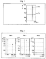
- FIG. 1 shows a memory cell array of a DRAM from 1024 Word lines in the X direction and 1024 bit lines in the Y direction. At every intersection of a word line with a Bit line is a memory cell, not shown intended.
- the memory cell array thus present has 1024 x 1024 memory cells and thus forms a 1 Mb memory array. 1 are to simplify the illustration a bit line BL and a word line WL in full lines shown.
- a complete test sequence at the wafer level for identification failed memory cells consist of one large number of individual tests. To simplify, let's assume that only three tests A, B and C in a complete Test sequence can be carried out as shown in FIG. 2 is illustrated.
- Fig. 2 gives an example in which after implementation respective tests A, B and C different memory cells or Bits are determined to be incorrect.
- a first two failed or faulty bits determined while in a second test B two individual failed Bits and a failed bit line detected while in the last test C a full word line is found to be defective.
- the addresses of the respective defective bits or bit lines and word lines are kept in a register while performing the Tests stored in real time. From Fig. 3 the content is one such registers can be seen after performing the first test.
- test A a first failed bit in a position 803/250 determined. Since no similar entry at 803 or 250, this failure is under the Y address 803 with hit value 1 and at X address 250 saved with hit value 1. The same applies to the Failure at location 630/799: under the Y address 630 the hit value 1 is stored, while under the X address 799 Hit value 1 is also recorded.
- Test B then follows. A single fancy Memory cell should be found here at 803/730. In the event that the same address pair is already in the respective hit values should be stored in the register be increased by 1 each. In the present case it is now only the row address 803 already exists. Therefore 803/730 entered in the register, and the hit value for the Y address 803 is increased to 2 because 803 for this Y address now there are two hits.
- Test B Another faulty memory cell is similar in Test B. to positions 803/250 and 630/799 from Test A at the position 402/128 determined.
- a special case occurs in Test B for a faulty one Bit line at X / 512 on. With a usual evaluation such a faulty bit line to an excessively large one Maintain registers, which in this case comprise 1024 stacks would. However, this can be the case with the semiconductor memory arrangement according to the invention through the application of a special Algorithm to be avoided: whenever the hit value one exceeds a certain threshold value, for example 3 , it is assumed that a complete spare column or spare line is to be used. In other words, if, for example, 3 or more hits for a Y address and 3 or more hits occur for an X address, so the entire column or row is "automatically" by a Bit line or word line replaced.
- a certain threshold value for example 3
- the information obtained after tests A, B and C. failed memory cell or bit lines and word lines can then be evaluated to determine the best possible assignment of spare memory cells or spare columns and spare rows to identify all failed memory cells or bit lines and word lines through redundant memory cells or to replace bit lines and word lines. This calculation can easily be done in the BIST computing unit be carried out on the semiconductor chip or also externally.
- Hit 3 for the X address means that a spare bit line must be used.
- the register can advantageously be used as an associative memory be carried out. Every hit value is by at least two bits are shown, and require approximately thirteen bits per address about twenty bits for a single entry in the register. Such an associative behavior can be found in on the order of 20 NAND gates and 20 XOR gates two inputs per register entry can be realized.
- the register needs a capacity that is sufficient the entire information of failed memory cells, that is at most the total number of redundant bit lines and the redundant word lines.
- Fig. 6 shows a block diagram for realizing the Semiconductor memory arrangement according to the invention: this exists from a large number of memory cell fields 1, 2, ..., n. Each of these memory cell fields 1, 2, ..., n is in the Set up way, as shown for example in Fig. 1 is. It is possible in each of the memory cell fields 1, 2, ..., n redundant bit lines and word lines with to provide corresponding memory cells. But it is the same also possible these redundant bit lines and word lines with the corresponding memory cells in a separate To accommodate memory cell array 10.
- the individual memory cell fields are tested in a test Control of their word lines and bit lines checked, around defective memory cells or word lines and Determine bit lines as explained above.
- the Results of this test are stored in a register 12. But it is also possible to see the results in error Save DRAM yourself. For example, when testing of memory field 1 the results in the still untested Storage field 10 are stored. However, this sets one highly redundant storage of information in advance.
Landscapes
- Engineering & Computer Science (AREA)
- Microelectronics & Electronic Packaging (AREA)
- Computer Hardware Design (AREA)
- For Increasing The Reliability Of Semiconductor Memories (AREA)
- Dram (AREA)
- Techniques For Improving Reliability Of Storages (AREA)
Abstract
Description
- Fig. 1
- eine Prinzipdarstellung eines Speicherzellenfeldes bei der erfindungsgemäßen Halbleiterspeicheranordnung,
- Fig. 2
- eine Darstellung für den Ablauf von drei Tests,
- Fig. 3 bis 5
- Hit-Werte, die bei den anhand der Fig. 2 durchgeführten Tests erhalten sind, und
- Fig. 6
- ein Blockschaltbild für den Aufbau der erfindungsgemäßen Halbleiterspeicheranordnung.
Claims (4)
- Halbleiterspeicheranordnung mit einem über Wortleitungen (WL) und Bitleitungen (BL) angesteuerten Speicherzellenfeld (1, 2, ..., n) aus einer Vielzahl von Speicherzellen und mit redundanten Speicherzellen, die bei einem Ausfall von Speicherzellen des Speicherzellenfeldes diese als Spare-Speicherzellen ersetzen, wobei die Speicherzellen des Speicherzellenfeldes und die Spare-Speicherzellen auf einem Halbleiterchip vorgesehen sind, in welchem zusätzlich eine BIST-Recheneinheit (14) vorgesehen ist, die den ausgefallenen Speicherzellen die Spare-Speicherzellen zuordnet und mit Registern (12) vorgesehen ist, in denen für die einzelnen Wortleitungen und Bitleitungen die Adressen der ausgefallenen Speicherzellen abspeicherbar sind,
gekennzeichnet durch
eine in der BIST-Recheneinheit (14) vorgesehene Zählereinheit (15), die für jede Adresse die Anzahl der ausgefallenen Speicherzellen als einen Hit-Wert bis zu einer oberen Grenze hochzählt, bei dessen Überschreitung die entsprechende Wortleitung bzw. Bitleitung ersetzt wird. - Halbleiterspeicheranordnung nach Anspruch 1,
dadurch gekennzeichnet,
daß das Register als Stapelregister ausgeführt ist. - Halbleiterspeicheranordnung nach Anspruch 2,
dadurch gekennzeichnet,
daß das Stapelregister als Assoziativspeicher aufgebaut ist. - Halbleiterspeicheranordnung nach einem der Ansprüche 1 bis 3,
dadurch gekennzeichnet,
daß dem Register (12) ein fehlerbehafteter Teil eines DRAMs zugeordnet ist, in welchem Teilergebnisse von Tests abspeicherbar sind.
Applications Claiming Priority (2)
| Application Number | Priority Date | Filing Date | Title |
|---|---|---|---|
| DE19917588 | 1999-04-19 | ||
| DE19917588A DE19917588A1 (de) | 1999-04-19 | 1999-04-19 | Halbleiterspeicheranordnung mit BIST |
Publications (2)
| Publication Number | Publication Date |
|---|---|
| EP1046993A1 true EP1046993A1 (de) | 2000-10-25 |
| EP1046993B1 EP1046993B1 (de) | 2003-02-19 |
Family
ID=7905049
Family Applications (1)
| Application Number | Title | Priority Date | Filing Date |
|---|---|---|---|
| EP00107305A Expired - Lifetime EP1046993B1 (de) | 1999-04-19 | 2000-04-04 | Halbleiterspeicheranordnung mit BIST |
Country Status (6)
| Country | Link |
|---|---|
| US (1) | US6295237B1 (de) |
| EP (1) | EP1046993B1 (de) |
| JP (1) | JP2000311497A (de) |
| KR (1) | KR100349989B1 (de) |
| DE (2) | DE19917588A1 (de) |
| TW (1) | TW466498B (de) |
Families Citing this family (20)
| Publication number | Priority date | Publication date | Assignee | Title |
|---|---|---|---|---|
| KR100375998B1 (ko) * | 2000-11-17 | 2003-03-15 | (주)실리콘세븐 | 자동 테스트 및 리페어 기능을 내장하는 반도체 메모리장치 및 그 방법 |
| JP2002319296A (ja) * | 2001-04-19 | 2002-10-31 | Nec Corp | 半導体装置及びシステム及び方法 |
| DE10120255C2 (de) * | 2001-04-25 | 2003-03-20 | Infineon Technologies Ag | Integrierter Halbleiterspeicher mit Selbsttest sowie Test-Anordnung mit Test-System und integriertem Halbleiterspeicher |
| JP4137474B2 (ja) | 2002-03-18 | 2008-08-20 | 富士通株式会社 | 自己テスト回路及び半導体記憶装置 |
| KR100472460B1 (ko) * | 2002-07-04 | 2005-03-10 | 삼성전자주식회사 | 메모리의 결함 복구 방법 및 그에 적합한 장치 |
| DE60208376T2 (de) * | 2002-10-07 | 2006-08-03 | Infineon Technologies Ag | Verfahren zum Speichern von Fehlern einer Speichervorrichtung in einem Diagnosefeld mit minimaler Speicherkapazität |
| EP1408516B1 (de) * | 2002-10-07 | 2006-06-21 | Infineon Technologies AG | Interface zum Durchbrennen von Schmelzsicherungen für ein Speicherchip |
| US7054206B2 (en) * | 2003-05-28 | 2006-05-30 | Infineon Technologies Ag | Sub-column-repair-circuit |
| US7225375B2 (en) * | 2004-03-31 | 2007-05-29 | International Business Machines Corporation | Method and apparatus for detecting array degradation and logic degradation |
| DE102004022327B4 (de) * | 2004-05-06 | 2006-04-27 | Infineon Technologies Ag | Integrierter Halbleiterspeicher |
| WO2006090440A1 (ja) * | 2005-02-23 | 2006-08-31 | Spansion Llc | 記憶装置の試験方法、および記憶装置 |
| WO2006090443A1 (ja) * | 2005-02-23 | 2006-08-31 | Spansion Llc | 記憶装置の冗長設定方法、および記憶装置 |
| US7130534B1 (en) * | 2005-04-21 | 2006-10-31 | Agilent Technologies, Inc. | Gas chromatograph having a radiant oven for analytical devices |
| KR20090002636A (ko) * | 2007-07-02 | 2009-01-09 | 삼성전자주식회사 | 비휘발성 메모리 장치 및 그것의 소거 방법 |
| KR101108133B1 (ko) | 2007-07-26 | 2012-01-31 | 가부시키가이샤 어드밴티스트 | 예비 라인 할당 장치, 메모리 구제 장치, 예비 라인 할당 방법, 메모리 제조 방법, 및 프로그램 |
| JP4877396B2 (ja) * | 2010-01-20 | 2012-02-15 | 日本電気株式会社 | メモリ障害処理システム、および、メモリ障害処理方法 |
| KR101932664B1 (ko) * | 2012-08-27 | 2018-12-26 | 삼성전자 주식회사 | 리던던시 셀을 포함하는 반도체 메모리 장치 및 시스템 |
| US20130117615A1 (en) * | 2011-11-07 | 2013-05-09 | Su-a Kim | Semiconductor memory device and system having redundancy cells |
| US9135100B2 (en) | 2013-03-14 | 2015-09-15 | Micron Technology, Inc. | Cooperative memory error detection and repair |
| CN112837736A (zh) * | 2021-03-16 | 2021-05-25 | 江苏时代全芯存储科技股份有限公司 | 记忆体装置以及其修补方法 |
Citations (1)
| Publication number | Priority date | Publication date | Assignee | Title |
|---|---|---|---|---|
| US6032264A (en) * | 1997-04-22 | 2000-02-29 | Micron Technology, Inc. | Apparatus and method implementing repairs on a memory device |
Family Cites Families (3)
| Publication number | Priority date | Publication date | Assignee | Title |
|---|---|---|---|---|
| JPH09306198A (ja) * | 1996-02-07 | 1997-11-28 | Lsi Logic Corp | 冗長列及び入/出力線を備えたasicメモリを修復するための方法 |
| US5987632A (en) * | 1997-05-07 | 1999-11-16 | Lsi Logic Corporation | Method of testing memory operations employing self-repair circuitry and permanently disabling memory locations |
| US6085334A (en) * | 1998-04-17 | 2000-07-04 | Motorola, Inc. | Method and apparatus for testing an integrated memory device |
-
1999
- 1999-04-19 DE DE19917588A patent/DE19917588A1/de not_active Withdrawn
-
2000
- 2000-04-04 EP EP00107305A patent/EP1046993B1/de not_active Expired - Lifetime
- 2000-04-04 DE DE50001262T patent/DE50001262D1/de not_active Expired - Lifetime
- 2000-04-11 TW TW089106695A patent/TW466498B/zh not_active IP Right Cessation
- 2000-04-17 JP JP2000115372A patent/JP2000311497A/ja active Pending
- 2000-04-19 US US09/553,127 patent/US6295237B1/en not_active Expired - Lifetime
- 2000-04-19 KR KR1020000020611A patent/KR100349989B1/ko not_active Expired - Fee Related
Patent Citations (1)
| Publication number | Priority date | Publication date | Assignee | Title |
|---|---|---|---|---|
| US6032264A (en) * | 1997-04-22 | 2000-02-29 | Micron Technology, Inc. | Apparatus and method implementing repairs on a memory device |
Non-Patent Citations (3)
| Title |
|---|
| BHAVSAR D K ET AL: "TESTABILITY STRATEGY OF THE ALPHA AXP 21164 MICROPROCESSOR", PROCEEDINGS OF THE INTERNATIONAL TEST CONFERENCE,US,NEW YORK, IEEE, 1994, pages 50 - 59, XP000519963, ISBN: 0-7803-2103-0 * |
| KOWARIK O: "SELF-REPAIRING SEMICONDUCTOR MEMORY CHIP WITH IMPROVED AVAILABILITY / RELIABILITY", PROCEEDINGS OF THE CUSTOM INTEGRATED CIRCUITS CONFERENCE,US,NEW YORK, IEEE, vol. CONF. 9, 1987, pages 598 - 601, XP000757371 * |
| RITTER J C ET AL: "BUILT-IN TEST PROCESSOR FOR SELF-TESTING REPAIRABLE RANDOM ACCESS MEMORIES", PROCEEDINGS OF THE INTERNATIONAL TEST CONFERENCE,US,WASHINGTON, IEEE COMP. SOC. PRESS, vol. CONF. 18, 1988, pages 1078 - 1084, XP000745843 * |
Also Published As
| Publication number | Publication date |
|---|---|
| KR100349989B1 (ko) | 2002-08-23 |
| TW466498B (en) | 2001-12-01 |
| DE50001262D1 (de) | 2003-03-27 |
| KR20010020761A (ko) | 2001-03-15 |
| JP2000311497A (ja) | 2000-11-07 |
| US6295237B1 (en) | 2001-09-25 |
| EP1046993B1 (de) | 2003-02-19 |
| DE19917588A1 (de) | 2000-11-02 |
Similar Documents
| Publication | Publication Date | Title |
|---|---|---|
| EP1046993B1 (de) | Halbleiterspeicheranordnung mit BIST | |
| EP1444699B1 (de) | Verfahren zur rekonfiguration eines speichers | |
| EP0378538B1 (de) | Anordnung und verfahren zur feststellung und lokalisierung von fehlerhaften schaltkreisen eines speicherbausteins | |
| DE3032630C2 (de) | Halbleiterspeicher aus Speicherbausteinen mit redundanten Speicherbereichen und Verfahren zu dessen Betrieb | |
| DE69411532T2 (de) | Verfahren zur Programmierung von Redundanzregistern in einer Zeilenredundanzschaltung für einen Halbleiterspeicherbaustein | |
| DE10225381A1 (de) | Verfahren und Vorrichtung zum Speichern von Speichertestinformantion | |
| EP1113362B1 (de) | Integrierter Halbleiterspeicher mit einer Speichereinheit zum Speichern von Adressen fehlerhafter Speicherzellen | |
| EP0843317B1 (de) | Verfahren zum Testen eines in Zellenfelder unterteilten Speicherchips im laufenden Betrieb eines Rechners unter Einhaltung von Echtzeitbedingungen | |
| DE10131388A1 (de) | Integrierter dynamischer Speicher und Verfahren zum Betrieb desselben | |
| DE19922786B4 (de) | Halbleiterspeicher mit Testeinrichtung | |
| DE69324020T2 (de) | Halbleiterspeicher mit redundanter Schaltung | |
| DE19830362A1 (de) | Halbleiterspeichervorrichtung | |
| DE10035705A1 (de) | Verfahren zum Analysieren des Ersatzes fehlerhafter Zellen in einem Speicher und Speichertestvorrichtung mit einem Fehleranalysator, der von dem Verfahren Gebrauch macht | |
| DE10331068A1 (de) | Verfahren zum Auslesen von Fehlerinformationen aus einem integrierten Baustein und integrierter Speicherbaustein | |
| DE102021117062A1 (de) | Speicherreparatur unter verwendung optimierter redundanznutzung | |
| DE19924153B4 (de) | Schaltungsanordnung zur Reparatur eines Halbleiterspeichers | |
| EP1071994B1 (de) | Speicheranordnung mit redundanten speicherzellen und verfahren zum zugriff auf redundante speicherzellen | |
| DE10229164A1 (de) | Speicherbaustein mit einem Datengenerator und einer Testlogik und Verfahren zum Testen von Speicherzellen eines Speicherbausteins | |
| DE10307027A1 (de) | Verfahren und Testeinrichtung zum Ermitteln einer Reparaturlösung für einen Speicherbaustein | |
| DE10016719A1 (de) | Integrierter Speicher und Verfahren zur Funktionsprüfung von Speicherzellen eines integrierten Speichers | |
| EP1100016B1 (de) | Speichereinrichtung mit Ersatz-Speicherzellen | |
| DE69319886T2 (de) | Halbleiterspeicher mit Speichermatrix, der mit einem einzigen Sektor assoziierte Redundantezellenspalte enthält | |
| DE10110272B4 (de) | Halbleiterspeicher | |
| DE10341555B4 (de) | Topographiekorrektur zum Testen redundanter Arrayelemente | |
| EP1141835B1 (de) | Integrierter speicher mit redundanz |
Legal Events
| Date | Code | Title | Description |
|---|---|---|---|
| PUAI | Public reference made under article 153(3) epc to a published international application that has entered the european phase |
Free format text: ORIGINAL CODE: 0009012 |
|
| AK | Designated contracting states |
Kind code of ref document: A1 Designated state(s): DE FR GB IE IT |
|
| AX | Request for extension of the european patent |
Free format text: AL;LT;LV;MK;RO;SI |
|
| 17P | Request for examination filed |
Effective date: 20001120 |
|
| AKX | Designation fees paid |
Free format text: DE FR GB IE IT |
|
| GRAH | Despatch of communication of intention to grant a patent |
Free format text: ORIGINAL CODE: EPIDOS IGRA |
|
| GRAH | Despatch of communication of intention to grant a patent |
Free format text: ORIGINAL CODE: EPIDOS IGRA |
|
| GRAA | (expected) grant |
Free format text: ORIGINAL CODE: 0009210 |
|
| AK | Designated contracting states |
Designated state(s): DE FR GB IE IT |
|
| PG25 | Lapsed in a contracting state [announced via postgrant information from national office to epo] |
Ref country code: IT Free format text: LAPSE BECAUSE OF FAILURE TO SUBMIT A TRANSLATION OF THE DESCRIPTION OR TO PAY THE FEE WITHIN THE PRESCRIBED TIME-LIMIT;WARNING: LAPSES OF ITALIAN PATENTS WITH EFFECTIVE DATE BEFORE 2007 MAY HAVE OCCURRED AT ANY TIME BEFORE 2007. THE CORRECT EFFECTIVE DATE MAY BE DIFFERENT FROM THE ONE RECORDED. Effective date: 20030219 Ref country code: FR Free format text: LAPSE BECAUSE OF FAILURE TO SUBMIT A TRANSLATION OF THE DESCRIPTION OR TO PAY THE FEE WITHIN THE PRESCRIBED TIME-LIMIT Effective date: 20030219 |
|
| REG | Reference to a national code |
Ref country code: GB Ref legal event code: FG4D Free format text: NOT ENGLISH |
|
| REG | Reference to a national code |
Ref country code: IE Ref legal event code: FG4D Free format text: GERMAN |
|
| REF | Corresponds to: |
Ref document number: 50001262 Country of ref document: DE Date of ref document: 20030327 Kind code of ref document: P |
|
| GBT | Gb: translation of ep patent filed (gb section 77(6)(a)/1977) | ||
| PLBE | No opposition filed within time limit |
Free format text: ORIGINAL CODE: 0009261 |
|
| STAA | Information on the status of an ep patent application or granted ep patent |
Free format text: STATUS: NO OPPOSITION FILED WITHIN TIME LIMIT |
|
| EN | Fr: translation not filed | ||
| 26N | No opposition filed |
Effective date: 20031120 |
|
| PGFP | Annual fee paid to national office [announced via postgrant information from national office to epo] |
Ref country code: GB Payment date: 20060420 Year of fee payment: 7 |
|
| GBPC | Gb: european patent ceased through non-payment of renewal fee |
Effective date: 20070404 |
|
| PG25 | Lapsed in a contracting state [announced via postgrant information from national office to epo] |
Ref country code: GB Free format text: LAPSE BECAUSE OF NON-PAYMENT OF DUE FEES Effective date: 20070404 |
|
| REG | Reference to a national code |
Ref country code: DE Ref legal event code: R081 Ref document number: 50001262 Country of ref document: DE Owner name: INFINEON TECHNOLOGIES AG, DE Free format text: FORMER OWNER: QIMONDA AG, 81739 MUENCHEN, DE Ref country code: DE Ref legal event code: R081 Ref document number: 50001262 Country of ref document: DE Owner name: POLARIS INNOVATIONS LTD., IE Free format text: FORMER OWNER: QIMONDA AG, 81739 MUENCHEN, DE |
|
| PGFP | Annual fee paid to national office [announced via postgrant information from national office to epo] |
Ref country code: DE Payment date: 20150616 Year of fee payment: 16 |
|
| PGFP | Annual fee paid to national office [announced via postgrant information from national office to epo] |
Ref country code: IE Payment date: 20150424 Year of fee payment: 16 |
|
| REG | Reference to a national code |
Ref country code: DE Ref legal event code: R081 Ref document number: 50001262 Country of ref document: DE Owner name: POLARIS INNOVATIONS LTD., IE Free format text: FORMER OWNER: INFINEON TECHNOLOGIES AG, 85579 NEUBIBERG, DE |
|
| REG | Reference to a national code |
Ref country code: DE Ref legal event code: R119 Ref document number: 50001262 Country of ref document: DE |
|
| REG | Reference to a national code |
Ref country code: IE Ref legal event code: MM4A |
|
| PG25 | Lapsed in a contracting state [announced via postgrant information from national office to epo] |
Ref country code: DE Free format text: LAPSE BECAUSE OF NON-PAYMENT OF DUE FEES Effective date: 20161101 |
|
| PG25 | Lapsed in a contracting state [announced via postgrant information from national office to epo] |
Ref country code: IE Free format text: LAPSE BECAUSE OF NON-PAYMENT OF DUE FEES Effective date: 20160404 |