EP1031055B1 - Optische anordnung im strahlengang eines konfokalen fluoreszenzmikroskops - Google Patents
Optische anordnung im strahlengang eines konfokalen fluoreszenzmikroskops Download PDFInfo
- Publication number
- EP1031055B1 EP1031055B1 EP99955690A EP99955690A EP1031055B1 EP 1031055 B1 EP1031055 B1 EP 1031055B1 EP 99955690 A EP99955690 A EP 99955690A EP 99955690 A EP99955690 A EP 99955690A EP 1031055 B1 EP1031055 B1 EP 1031055B1
- Authority
- EP
- European Patent Office
- Prior art keywords
- mirror
- confocal fluorescence
- beam path
- light
- scanning microscope
- Prior art date
- Legal status (The legal status is an assumption and is not a legal conclusion. Google has not performed a legal analysis and makes no representation as to the accuracy of the status listed.)
- Revoked
Links
- 230000003287 optical effect Effects 0.000 title claims description 16
- 238000001514 detection method Methods 0.000 claims description 26
- 238000005286 illumination Methods 0.000 claims description 25
- 230000005540 biological transmission Effects 0.000 claims description 3
- 230000005284 excitation Effects 0.000 description 32
- 238000001218 confocal laser scanning microscopy Methods 0.000 description 3
- 238000005259 measurement Methods 0.000 description 2
- 238000000926 separation method Methods 0.000 description 2
- 230000004888 barrier function Effects 0.000 description 1
- 230000000903 blocking effect Effects 0.000 description 1
- 239000011248 coating agent Substances 0.000 description 1
- 238000000576 coating method Methods 0.000 description 1
- 230000000052 comparative effect Effects 0.000 description 1
- 238000010276 construction Methods 0.000 description 1
- 230000001419 dependent effect Effects 0.000 description 1
- 238000011161 development Methods 0.000 description 1
- 230000018109 developmental process Effects 0.000 description 1
- 238000006073 displacement reaction Methods 0.000 description 1
- 230000002349 favourable effect Effects 0.000 description 1
- 238000000034 method Methods 0.000 description 1
- 230000011514 reflex Effects 0.000 description 1
- 238000004441 surface measurement Methods 0.000 description 1
Images

Classifications
-
- G—PHYSICS
- G01—MEASURING; TESTING
- G01N—INVESTIGATING OR ANALYSING MATERIALS BY DETERMINING THEIR CHEMICAL OR PHYSICAL PROPERTIES
- G01N21/00—Investigating or analysing materials by the use of optical means, i.e. using sub-millimetre waves, infrared, visible or ultraviolet light
- G01N21/62—Systems in which the material investigated is excited whereby it emits light or causes a change in wavelength of the incident light
- G01N21/63—Systems in which the material investigated is excited whereby it emits light or causes a change in wavelength of the incident light optically excited
- G01N21/64—Fluorescence; Phosphorescence
- G01N21/645—Specially adapted constructive features of fluorimeters
- G01N21/6456—Spatial resolved fluorescence measurements; Imaging
- G01N21/6458—Fluorescence microscopy
-
- G—PHYSICS
- G02—OPTICS
- G02B—OPTICAL ELEMENTS, SYSTEMS OR APPARATUS
- G02B21/00—Microscopes
- G02B21/0004—Microscopes specially adapted for specific applications
- G02B21/002—Scanning microscopes
- G02B21/0024—Confocal scanning microscopes (CSOMs) or confocal "macroscopes"; Accessories which are not restricted to use with CSOMs, e.g. sample holders
- G02B21/0052—Optical details of the image generation
- G02B21/0076—Optical details of the image generation arrangements using fluorescence or luminescence
-
- G—PHYSICS
- G02—OPTICS
- G02B—OPTICAL ELEMENTS, SYSTEMS OR APPARATUS
- G02B21/00—Microscopes
- G02B21/0004—Microscopes specially adapted for specific applications
- G02B21/002—Scanning microscopes
- G02B21/0024—Confocal scanning microscopes (CSOMs) or confocal "macroscopes"; Accessories which are not restricted to use with CSOMs, e.g. sample holders
- G02B21/008—Details of detection or image processing, including general computer control
Definitions
- the invention relates to an optical arrangement in the beam path of a confocal fluorescence microscope, comprising at least one laser light source, a device arranged in the illumination / detection beam path for separating the excitation light reflected from the object from the fluorescence light emitted by the object, an objective arranged between the device and the object the device downstream in the detection beam path detector.
- dichroic beam splitters to separate the excitation light reflected from the object from the fluorescent light emitted by the object.
- multiple dichroic beam splitters are used accordingly.
- the beam splitters used in practice are generally expensive.
- these beam splitters for quantitative comparative measurements of high precision and high dynamic range only a little, especially since these beam splitters u.a. are also temperature dependent.
- dichroic beam splitters have transmission losses of about 10% for detection.
- the entire numerical aperture is used for illumination or scanning. This leads to a focus of illumination that is very small in the lateral direction, so that longer recording times are required. For applications in which the resolution plays a minor role, this procedure is disadvantageous because of the longer recording times.
- the present invention is based on the object of designing and further developing an optical arrangement in the beam path of a confocal fluorescence microscope in such a way that it is possible to increase the fluorescence yield with a simple construction compared to the generic arrangement with conventional dichroic beam splitter.
- the inventive optical arrangement in the beam path of a confocal fluorescence microscope solves the above problem by the features of claim 1.
- the aforementioned optical arrangement is characterized in that the device comprises a mirror and that the mirror in the illumination / detection beam path is arranged and dimensioned in that, for the dark field illumination of the object, it does not expand the one coming from the laser light source Reflected excitation beam into the lens and the coming of the object fluorescent light with full numerical aperture - reduced by the effective in the detection beam path cross-section of the mirror - pass in the direction of the detector.
- the device comprises a mirror and that the mirror in the illumination / detection beam path is arranged and dimensioned such that it reflects the dark field illumination of the object coming from the laser light source, not expanded excitation beam into the lens and the From the object coming fluorescent light with full numerical aperture - reduced by the effective in the detection beam path cross-section of the mirror - can pass in the direction of the detector.
- the device for separating the excitation light reflected by the object from the fluorescent light emitted by the object - instead of a conventional dichroic beam splitter - can be a mirror which is arranged in the illumination / detection beam path.
- This mirror is so - sufficiently small - to be dimensioned so that it for dark field illumination of the object from the laser light source, not expanded excitation beam reflected into the lens and the coming of the object fluorescent light with full numerical aperture can pass in the direction of the detector, the Fluorescence light is reduced by the effective in the detection beam path cross-section of the mirror.
- the main reflection of the excitation light reflected by the object is reflected out of the detection beam path in an advantageous manner at the mirror.
- the mirror is dimensioned or made small such that it causes a loss of about 1% for the fluorescent light to be detected in the detection beam path. This enables efficient detection with a particularly high dynamic range.
- the mirror used here could be embodied as part of a particularly simple embodiment as an independent component, wherein the mirror is in turn carried by a holder.
- the use of a conventional beam splitter eliminates completely, since only the small mirror is arranged in the beam path at the appropriate point.
- the mirror could be embodied as a preferably integral mirrored region of a-otherwise conventional-beam splitter, the mirror or the mirrored region being arranged or formed at least substantially in the middle of the beam splitter.
- This small - integral - mirror could be approximately round or elliptical or oval.
- this is a mirrored area in the middle of a beam splitter which, like an isolated mirror, reflects the non-expanded excitation beam into the lens. Again, illumination takes place with a very small numerical aperture to promote dynamics.
- the non-reflecting region of the beam splitter could have approximately 10% reflection and 90% transmission in the direction of the detector. Specifically, this could be an anti-reflection (AR) coating on the side of the beam splitter facing the detector.
- This beam splitter allows the fluorescent light to pass in the direction of the detector in accordance with the customary-infinite-beam path with the full numerical aperture-reduced by the fluorescent light striking the mirrored region. Due to the mirrored area, an extremely low loss arises for the fluorescent light to be detected, namely as a function of the size of the mirror. Here, losses of only 1% can be realized, which leads to the already mentioned high dynamics.
- the non-reflecting region of the beam splitter could be designed and optionally coated such that the optical properties of the non-reflecting region of the beam splitter are at least largely independent of temperature. The reproducibility of the measurement is favored thereby.
- the object could be arranged obliquely. This means that the object itself is not arranged orthogonal to the optical axis, so that there is a separate beam path for the back-reflected excitation light, which is at least slightly - spatially - offset from the illumination beam path.
- Conventional light traps can be readily arranged in this special beam path in order to effectively block out the back-reflected excitation light.
- the object is movable in its plane so that the illuminated object area always the has the same distance to the lens.
- the light reflected and / or scattered on the object does not pass back into the laser light source but via the special beam path into a light trap.
- the mirror could-in the context of an embodiment as an insulated component-have an absorbing region for absorbing the excitation light scattered and / or reflected by the object.
- the provision of special light traps is no longer necessary, resulting in a spatial reduction of the arrangement.
- the mirror could-in the context of a round or elliptical or oval configuration-have a reflective or reflecting area and an absorbing area.
- the beam splitter prefferably has, in addition to the mirrored region, an absorbing region for absorbing the excitation light scattered and / or reflected by the object. Even in the context of such an embodiment, the provision of a special light trap can be omitted, so that this embodiment also has the advantage of being able to build the arrangement with minimal space requirements.
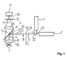
- Fig. 1 shows a schematic representation of an embodiment of an optical arrangement in the beam path of a confocal fluorescence microscope, said arrangement - in the embodiment chosen here - two laser light sources 1, 2, arranged in the illumination / detection beam path 3, 4, 5 means 6 for Separation of the excitation light 8 reflected by the object 7 from the fluorescent light 9 emitted by the object 7, an objective 10 arranged between the device 6 and the object 7 and a detector 11 arranged downstream of the device 6 in the detection beam path 5.
- Fig. 1 shows schematically that the excitation light 8 passes through a beam combiner 12 to the device 6, is reflected by this in the lens 10 and from there to the object 7 passes.
- the fluorescent light 9 in turn passes through the objective 10 to the device 6, passes it with the exception of the reflective region formed in the manner according to the invention as a mirror 13 and passes to the detector 11 via a tube lens 14, a blocking filter wheel 15 and a detection pinhole 16.
- the device 6 comprises a mirror 13, wherein the mirror 13 in the illumination / detection beam path 3, 4, 5 is arranged and dimensioned such that it for the dark field illumination of the object 7 from the laser light sources 1, 2, not expanded excitation beam or the excitation light 8 is reflected in the lens 10 and the coming of the object 7 fluorescent light 9 with full numerical aperture - reduced by the effective in the detection beam 4, 5 cross section of the mirror 13 in the direction of the detector 11 passes.
- the device 6 is designed as a beam splitter, wherein the mirror 13 is integrated there in the middle.
- Fig. 3 shows an alternative embodiment of the device 6 in that it is simply designed as a single mirror 13, wherein the mirror 13 is an independent component.
- the mirror 13 could have an overall mirrored surface as shown in FIG.
- the mirror 13 is likewise embodied as a separate component, the surface of the mirror 13 being subdivided into a reflecting mirror surface 17 and into an absorbing surface 18.
- the back reflections or the back-reflected excitation light 19 can be rendered "harmless", that the sample or the object 7 is skewed, that is not arranged orthogonal to the optical axis 23.
- the back-reflected excitation light 19 is slightly offset from the illumination beam path 20 or the beam path of the excitation light 8, so that the back-reflected excitation light 19 is reflected back along its own beam path 21.
- a light trap 22 is arranged at a suitable location, which is due to the orientation of the beam path 21 away from the illumination beam path 20 and the excitation light 8.
Landscapes
- Physics & Mathematics (AREA)
- Chemical & Material Sciences (AREA)
- Analytical Chemistry (AREA)
- General Physics & Mathematics (AREA)
- Optics & Photonics (AREA)
- Health & Medical Sciences (AREA)
- Computer Vision & Pattern Recognition (AREA)
- General Engineering & Computer Science (AREA)
- Engineering & Computer Science (AREA)
- Nuclear Medicine, Radiotherapy & Molecular Imaging (AREA)
- Life Sciences & Earth Sciences (AREA)
- Biochemistry (AREA)
- General Health & Medical Sciences (AREA)
- Immunology (AREA)
- Pathology (AREA)
- Microscoopes, Condenser (AREA)
- Investigating, Analyzing Materials By Fluorescence Or Luminescence (AREA)
Applications Claiming Priority (3)
| Application Number | Priority Date | Filing Date | Title |
|---|---|---|---|
| DE19842153A DE19842153C2 (de) | 1998-09-15 | 1998-09-15 | Fluoreszenzmikroskop |
| DE19842153 | 1998-09-15 | ||
| PCT/DE1999/002910 WO2000016149A1 (de) | 1998-09-15 | 1999-09-13 | Optische anordnung im strahlengang eines konfokalen fluoreszenzmikroskops |
Publications (2)
| Publication Number | Publication Date |
|---|---|
| EP1031055A1 EP1031055A1 (de) | 2000-08-30 |
| EP1031055B1 true EP1031055B1 (de) | 2006-01-25 |
Family
ID=7880995
Family Applications (1)
| Application Number | Title | Priority Date | Filing Date |
|---|---|---|---|
| EP99955690A Revoked EP1031055B1 (de) | 1998-09-15 | 1999-09-13 | Optische anordnung im strahlengang eines konfokalen fluoreszenzmikroskops |
Country Status (5)
| Country | Link |
|---|---|
| US (1) | US6785302B1 (enExample) |
| EP (1) | EP1031055B1 (enExample) |
| JP (1) | JP4197395B2 (enExample) |
| DE (2) | DE19842153C2 (enExample) |
| WO (1) | WO2000016149A1 (enExample) |
Families Citing this family (21)
| Publication number | Priority date | Publication date | Assignee | Title |
|---|---|---|---|---|
| EP1157268B1 (en) * | 1999-02-26 | 2007-11-21 | Perkinelmer Life Sciences, Inc. | Imaging system for an optical scanner |
| US6355934B1 (en) | 1999-02-26 | 2002-03-12 | Packard Biochip Technologies | Imaging system for an optical scanner |
| DE19923822A1 (de) † | 1999-05-19 | 2000-11-23 | Zeiss Carl Jena Gmbh | Scannende Anordnung, vorzugsweise zur Erfassung von Fluoreszenzlicht |
| US6795189B2 (en) * | 2000-06-15 | 2004-09-21 | Packard Instrument Company | Universal microplate analyzer |
| EP1164402B1 (de) * | 2000-06-17 | 2010-04-28 | Leica Microsystems CMS GmbH | Scanmikroskop mit mehrbandiger Beleuchtung und optisches Bauelement für ein Scanmikroskop mit mehrbandiger Beleuchtung |
| FR2813121A1 (fr) * | 2000-08-21 | 2002-02-22 | Claude Weisbuch | Dispositif perfectionne de support d'elements chromophores |
| US6826424B1 (en) * | 2000-12-19 | 2004-11-30 | Haishan Zeng | Methods and apparatus for fluorescence and reflectance imaging and spectroscopy and for contemporaneous measurements of electromagnetic radiation with multiple measuring devices |
| US6750457B2 (en) * | 2001-08-29 | 2004-06-15 | Becton Dickinson And Company | System for high throughput analysis |
| DE10143481A1 (de) * | 2001-09-05 | 2003-03-20 | Europ Lab Molekularbiolog | Mikroskop |
| DE10144062B4 (de) * | 2001-09-07 | 2010-05-27 | Leica Microsystems Ag | Mikroskop mit einer Beleuchtungseinspiegelung |
| US6888148B2 (en) * | 2001-12-10 | 2005-05-03 | Carl Zeiss Jena Gmbh | Arrangement for the optical capture of excited and /or back scattered light beam in a sample |
| DE10327987A1 (de) * | 2003-06-21 | 2005-01-20 | MAX-PLANCK-Gesellschaft zur Förderung der Wissenschaften e.V. | Konfokales optisches System |
| DE10332073A1 (de) * | 2003-07-11 | 2005-02-10 | Carl Zeiss Jena Gmbh | Anordnung zur optischen Erfassung von in einer Probe angeregter und / oder rückgestreuter Lichtstrahlung mit Doppelobjektivanordnung |
| FR2860606B1 (fr) * | 2003-10-07 | 2006-01-21 | Thales Sa | Convertisseur multimode-monomode, en particulier pour source laser a fibre amplificatrice multimode |
| DE102004038321B4 (de) | 2003-11-21 | 2022-05-25 | Leica Microsystems Cms Gmbh | Lichtfalle |
| FR2869686B1 (fr) * | 2003-12-11 | 2009-06-05 | Flowgene Sa | Detecteur de lumiere a chambre elliptique |
| DE102006056429B3 (de) * | 2006-11-28 | 2008-02-14 | Leica Microsystems Cms Gmbh | Lasermikroskop mit räumlich trennendem Strahlteiler |
| DE102007024074B4 (de) | 2007-05-22 | 2022-09-15 | Leica Microsystems Cms Gmbh | Mikroskop |
| JP6058977B2 (ja) * | 2012-11-15 | 2017-01-11 | シャープ株式会社 | 蛍光検出装置 |
| WO2015005073A1 (ja) * | 2013-07-11 | 2015-01-15 | 株式会社島津製作所 | ラマン分光分析装置 |
| EP3542710A1 (de) * | 2018-03-23 | 2019-09-25 | JenLab GmbH | Multimodales bildgebungssystem und verfahren zur nicht-invasiven untersuchung eines untersuchungsobjekts |
Citations (1)
| Publication number | Priority date | Publication date | Assignee | Title |
|---|---|---|---|---|
| US5192980A (en) * | 1990-06-27 | 1993-03-09 | A. E. Dixon | Apparatus and method for method for spatially- and spectrally-resolved measurements |
Family Cites Families (19)
| Publication number | Priority date | Publication date | Assignee | Title |
|---|---|---|---|---|
| US4744663A (en) * | 1984-12-14 | 1988-05-17 | Nippon Kogaku K.K. | Pattern position detection apparatus using laser beam |
| DE3742806A1 (de) * | 1987-12-17 | 1989-07-13 | Zeiss Carl Fa | Verfahren und vorrichtung zur erzeugung von fluoreszenzbildern |
| JPH03269405A (ja) | 1990-03-19 | 1991-12-02 | Fujitsu Ltd | 蛍光顕微鏡 |
| US5127730A (en) * | 1990-08-10 | 1992-07-07 | Regents Of The University Of Minnesota | Multi-color laser scanning confocal imaging system |
| USH1344H (en) * | 1990-10-09 | 1994-08-02 | The United States Of America As Represented By The Secretary Of The Army | Portable automatic sensor for toxic gases |
| GB2254444B (en) | 1991-03-25 | 1994-06-15 | Birkbeck College | Laser microscopy |
| CH685650A5 (de) * | 1991-07-20 | 1995-08-31 | Tencor Instruments | Einrichtung für Oberflächeninspektionen. |
| JP3102938B2 (ja) * | 1991-12-30 | 2000-10-23 | シスメックス株式会社 | 粒子画像分析装置 |
| DE4243144B4 (de) * | 1992-12-19 | 2008-08-21 | BRUKER OPTICS, Inc., Billerica | Objektiv für ein FT-Raman-Mikroskop |
| JP3144513B2 (ja) * | 1993-06-17 | 2001-03-12 | 富士写真フイルム株式会社 | 蛍光顕微鏡 |
| DE4343076C2 (de) * | 1993-12-16 | 1997-04-03 | Phototherm Dr Petry Gmbh | Vorrichtung zum photothermischen Prüfen einer Oberfläche eines insbesondere bewegten Gegenstandes |
| US5734498A (en) * | 1994-05-09 | 1998-03-31 | The Regents Of The University Of California | Illuminator elements for conventional light microscopes |
| JP3537205B2 (ja) * | 1995-02-02 | 2004-06-14 | オリンパス株式会社 | 顕微鏡装置 |
| JPH09281045A (ja) | 1996-04-10 | 1997-10-31 | Kdk Corp | メバロン酸の光学的測定方法 |
| JPH1096862A (ja) * | 1996-09-20 | 1998-04-14 | Bunshi Bio Photonics Kenkyusho:Kk | 落射蛍光顕微鏡装置 |
| JP3269405B2 (ja) | 1996-10-08 | 2002-03-25 | 株式会社東京精密 | 数値制御工作機械の自動測定装置 |
| JPH10142507A (ja) * | 1996-11-11 | 1998-05-29 | Olympus Optical Co Ltd | レーザ走査顕微鏡 |
| JPH1198372A (ja) * | 1997-09-18 | 1999-04-09 | Olympus Optical Co Ltd | 色調整方法 |
| US6445491B2 (en) * | 1999-01-29 | 2002-09-03 | Irma America, Inc. | Method and apparatus for optical sectioning and imaging using time-gated parametric image amplification |
-
1998
- 1998-09-15 DE DE19842153A patent/DE19842153C2/de not_active Revoked
-
1999
- 1999-09-13 JP JP2000570627A patent/JP4197395B2/ja not_active Expired - Lifetime
- 1999-09-13 EP EP99955690A patent/EP1031055B1/de not_active Revoked
- 1999-09-13 DE DE59913082T patent/DE59913082D1/de not_active Expired - Lifetime
- 1999-09-13 WO PCT/DE1999/002910 patent/WO2000016149A1/de not_active Ceased
- 1999-09-13 US US09/554,083 patent/US6785302B1/en not_active Expired - Lifetime
Patent Citations (1)
| Publication number | Priority date | Publication date | Assignee | Title |
|---|---|---|---|---|
| US5192980A (en) * | 1990-06-27 | 1993-03-09 | A. E. Dixon | Apparatus and method for method for spatially- and spectrally-resolved measurements |
Also Published As
| Publication number | Publication date |
|---|---|
| DE59913082D1 (de) | 2006-04-13 |
| JP2002525651A (ja) | 2002-08-13 |
| DE19842153C2 (de) | 2003-07-31 |
| WO2000016149A1 (de) | 2000-03-23 |
| EP1031055A1 (de) | 2000-08-30 |
| JP4197395B2 (ja) | 2008-12-17 |
| DE19842153A1 (de) | 2000-03-16 |
| US6785302B1 (en) | 2004-08-31 |
Similar Documents
| Publication | Publication Date | Title |
|---|---|---|
| EP1031055B1 (de) | Optische anordnung im strahlengang eines konfokalen fluoreszenzmikroskops | |
| EP3262452B1 (de) | Vorrichtung und verfahren zum detektieren von licht | |
| EP1053497B1 (de) | Vorrichtung zur gleichzeitigen detektion mehrerer spektralbereiche eines lichtstrahls | |
| EP0978009B1 (de) | Anordnung zum kalibrieren eines laserscanmikroskops | |
| EP0264404B1 (de) | Vorrichtung zum selbsttaetigen fokussieren eines auflichtmikroskopes | |
| WO2009024529A1 (de) | Sted-fluoreszenzmikroskopie mit zweiphotonen-anregung | |
| DE102012019472A1 (de) | Optische Filtervorrichtung, insbesondere für Mikroskope | |
| DE2323593C3 (de) | Laser-Doppler-Anemometer | |
| EP1122574B1 (de) | Mikroskop-Aufbau | |
| DE19949272A1 (de) | Konfokales Laserscan-Mikroskop | |
| EP3084502B1 (de) | Mehrfarben-scanning-mikroskop | |
| DE102015102631A1 (de) | Vorrichtung und Verfahren zum Detektieren von Licht | |
| DE102004032953A1 (de) | Phasenfilter | |
| DE10300157B4 (de) | Konfokales 4-Pi-Mikroskop und Verfahren zur konfokalen 4-Pi-Mikroskopie | |
| EP1698929B1 (de) | Objektiv und Mikroskop | |
| DE10021379A1 (de) | Optische Messanordnung insbesondere zur Schichtdickenmessung | |
| EP2784564A1 (de) | Lichtmikroskop und Verfahren zum Untersuchen einer mikroskopischen Probe | |
| DE102004038321A1 (de) | Lichtfalle | |
| EP1102101A1 (de) | Laserscanmikroskop | |
| DE102022117536A1 (de) | Vorrichtung zur chromatisch konfokalen Messung von Abständen | |
| WO2007121864A1 (de) | Laser-scanning-mikroskop mit hauptstrahlteiler zur räumlichen trennung von beleuchtungs- und detektionsstrahlung | |
| DE10202466B4 (de) | Objektträger für die Fluoreszenzmikroskopie | |
| EP1049952B1 (de) | Anordnung zur optischen abtastung eines objekts | |
| DE102006011277A1 (de) | Laser-Scanning-Mikroskop und Laser-Scanning-Mikroskopierverfahren | |
| DE102013018672A1 (de) | Multispot-scanning mikroskop |
Legal Events
| Date | Code | Title | Description |
|---|---|---|---|
| PUAI | Public reference made under article 153(3) epc to a published international application that has entered the european phase |
Free format text: ORIGINAL CODE: 0009012 |
|
| 17P | Request for examination filed |
Effective date: 20000429 |
|
| AK | Designated contracting states |
Kind code of ref document: A1 Designated state(s): AT BE CH CY DE DK ES FI FR GB GR IE IT LI LU MC NL PT SE |
|
| 17Q | First examination report despatched |
Effective date: 20030818 |
|
| RAP1 | Party data changed (applicant data changed or rights of an application transferred) |
Owner name: LEICA MICROSYSTEMS HEIDELBERG GMBH |
|
| RBV | Designated contracting states (corrected) |
Designated state(s): CH DE FR GB LI |
|
| GRAP | Despatch of communication of intention to grant a patent |
Free format text: ORIGINAL CODE: EPIDOSNIGR1 |
|
| GRAS | Grant fee paid |
Free format text: ORIGINAL CODE: EPIDOSNIGR3 |
|
| GRAA | (expected) grant |
Free format text: ORIGINAL CODE: 0009210 |
|
| AK | Designated contracting states |
Kind code of ref document: B1 Designated state(s): CH DE FR GB LI |
|
| REG | Reference to a national code |
Ref country code: GB Ref legal event code: FG4D Free format text: NOT ENGLISH |
|
| REG | Reference to a national code |
Ref country code: CH Ref legal event code: EP |
|
| REF | Corresponds to: |
Ref document number: 59913082 Country of ref document: DE Date of ref document: 20060413 Kind code of ref document: P |
|
| GBT | Gb: translation of ep patent filed (gb section 77(6)(a)/1977) |
Effective date: 20060327 |
|
| RAP2 | Party data changed (patent owner data changed or rights of a patent transferred) |
Owner name: LEICA MICROSYSTEMS CMS GMBH |
|
| ET | Fr: translation filed | ||
| PG25 | Lapsed in a contracting state [announced via postgrant information from national office to epo] |
Ref country code: LI Free format text: LAPSE BECAUSE OF NON-PAYMENT OF DUE FEES Effective date: 20060930 Ref country code: CH Free format text: LAPSE BECAUSE OF NON-PAYMENT OF DUE FEES Effective date: 20060930 |
|
| PLBI | Opposition filed |
Free format text: ORIGINAL CODE: 0009260 |
|
| PLAX | Notice of opposition and request to file observation + time limit sent |
Free format text: ORIGINAL CODE: EPIDOSNOBS2 |
|
| 26 | Opposition filed |
Opponent name: CARL ZEISS JENA GMBH Effective date: 20061020 |
|
| REG | Reference to a national code |
Ref country code: FR Ref legal event code: TP |
|
| PLBB | Reply of patent proprietor to notice(s) of opposition received |
Free format text: ORIGINAL CODE: EPIDOSNOBS3 |
|
| REG | Reference to a national code |
Ref country code: GB Ref legal event code: 732E |
|
| REG | Reference to a national code |
Ref country code: CH Ref legal event code: PL |
|
| REG | Reference to a national code |
Ref country code: DE Ref legal event code: R103 Ref document number: 59913082 Country of ref document: DE Ref country code: DE Ref legal event code: R064 Ref document number: 59913082 Country of ref document: DE |
|
| PGFP | Annual fee paid to national office [announced via postgrant information from national office to epo] |
Ref country code: DE Payment date: 20110923 Year of fee payment: 13 Ref country code: FR Payment date: 20110928 Year of fee payment: 13 Ref country code: GB Payment date: 20110920 Year of fee payment: 13 |
|
| RDAF | Communication despatched that patent is revoked |
Free format text: ORIGINAL CODE: EPIDOSNREV1 |
|
| RDAG | Patent revoked |
Free format text: ORIGINAL CODE: 0009271 |
|
| STAA | Information on the status of an ep patent application or granted ep patent |
Free format text: STATUS: PATENT REVOKED |
|
| 27W | Patent revoked |
Effective date: 20111110 |
|
| GBPR | Gb: patent revoked under art. 102 of the ep convention designating the uk as contracting state |
Effective date: 20111110 |
|
| REG | Reference to a national code |
Ref country code: DE Ref legal event code: R107 Ref document number: 59913082 Country of ref document: DE Effective date: 20120614 |