EP1011127A2 - Chipverbindungsdüse - Google Patents
Chipverbindungsdüse Download PDFInfo
- Publication number
- EP1011127A2 EP1011127A2 EP99124956A EP99124956A EP1011127A2 EP 1011127 A2 EP1011127 A2 EP 1011127A2 EP 99124956 A EP99124956 A EP 99124956A EP 99124956 A EP99124956 A EP 99124956A EP 1011127 A2 EP1011127 A2 EP 1011127A2
- Authority
- EP
- European Patent Office
- Prior art keywords
- chip
- nozzle
- junction
- mirror surface
- center
- Prior art date
- Legal status (The legal status is an assumption and is not a legal conclusion. Google has not performed a legal analysis and makes no representation as to the accuracy of the status listed.)
- Granted
Links
Images


Classifications
-
- H—ELECTRICITY
- H01—ELECTRIC ELEMENTS
- H01L—SEMICONDUCTOR DEVICES NOT COVERED BY CLASS H10
- H01L21/00—Processes or apparatus adapted for the manufacture or treatment of semiconductor or solid state devices or of parts thereof
- H01L21/67—Apparatus specially adapted for handling semiconductor or electric solid state devices during manufacture or treatment thereof; Apparatus specially adapted for handling wafers during manufacture or treatment of semiconductor or electric solid state devices or components ; Apparatus not specifically provided for elsewhere
- H01L21/67005—Apparatus not specifically provided for elsewhere
- H01L21/67011—Apparatus for manufacture or treatment
- H01L21/67144—Apparatus for mounting on conductive members, e.g. leadframes or conductors on insulating substrates
-
- H—ELECTRICITY
- H01—ELECTRIC ELEMENTS
- H01L—SEMICONDUCTOR DEVICES NOT COVERED BY CLASS H10
- H01L2224/00—Indexing scheme for arrangements for connecting or disconnecting semiconductor or solid-state bodies and methods related thereto as covered by H01L24/00
- H01L2224/01—Means for bonding being attached to, or being formed on, the surface to be connected, e.g. chip-to-package, die-attach, "first-level" interconnects; Manufacturing methods related thereto
- H01L2224/10—Bump connectors; Manufacturing methods related thereto
- H01L2224/15—Structure, shape, material or disposition of the bump connectors after the connecting process
- H01L2224/16—Structure, shape, material or disposition of the bump connectors after the connecting process of an individual bump connector
-
- H—ELECTRICITY
- H01—ELECTRIC ELEMENTS
- H01L—SEMICONDUCTOR DEVICES NOT COVERED BY CLASS H10
- H01L2224/00—Indexing scheme for arrangements for connecting or disconnecting semiconductor or solid-state bodies and methods related thereto as covered by H01L24/00
- H01L2224/74—Apparatus for manufacturing arrangements for connecting or disconnecting semiconductor or solid-state bodies and for methods related thereto
- H01L2224/75—Apparatus for connecting with bump connectors or layer connectors
- H01L2224/7525—Means for applying energy, e.g. heating means
- H01L2224/753—Means for applying energy, e.g. heating means by means of pressure
- H01L2224/75301—Bonding head
- H01L2224/75302—Shape
-
- H—ELECTRICITY
- H01—ELECTRIC ELEMENTS
- H01L—SEMICONDUCTOR DEVICES NOT COVERED BY CLASS H10
- H01L2924/00—Indexing scheme for arrangements or methods for connecting or disconnecting semiconductor or solid-state bodies as covered by H01L24/00
- H01L2924/0001—Technical content checked by a classifier
- H01L2924/00014—Technical content checked by a classifier the subject-matter covered by the group, the symbol of which is combined with the symbol of this group, being disclosed without further technical details
-
- H—ELECTRICITY
- H01—ELECTRIC ELEMENTS
- H01L—SEMICONDUCTOR DEVICES NOT COVERED BY CLASS H10
- H01L2924/00—Indexing scheme for arrangements or methods for connecting or disconnecting semiconductor or solid-state bodies as covered by H01L24/00
- H01L2924/01—Chemical elements
- H01L2924/01079—Gold [Au]
-
- H—ELECTRICITY
- H01—ELECTRIC ELEMENTS
- H01L—SEMICONDUCTOR DEVICES NOT COVERED BY CLASS H10
- H01L2924/00—Indexing scheme for arrangements or methods for connecting or disconnecting semiconductor or solid-state bodies as covered by H01L24/00
- H01L2924/30—Technical effects
- H01L2924/301—Electrical effects
- H01L2924/3011—Impedance
Definitions
- the present invention relates to a chip junction nozzle by which, when semiconductor circuit elements, or the like, are produced, a chip of the semiconductor, SAW element, and the similar element, is taken out of a supply apparatus and is jointed onto a printed circuit board by high frequency bonding, or the like.
- the chip of the object is one used as face down mounting by a flip chip method.
- a chip of the semiconductors, SAW elements, and the like, prepared in the supply apparatus is individually taken out, and the chip is moved to a temporary placement base by a moving nozzle provided with a means which can move the chip in the X, Y, Z directions.
- the chip prepared in the supply apparatus is a face-up one
- the chip is flipped such that the chip assumes a face down posture between the moving means and the movement process, and when the chip is a face down one, only the movement is conducted.
- the chip 1 is moved to the temporary placement board 10 as shown in Fig. 20(A). Then, the position of the chip 1 is corrected as shown in Fig. 20(B) by four centering claws 11, in which respective one of the front and rear, and left and right, settled on the temporary placement base, is moved. Then, as shown in Fig. 20(C), the chip 1 on the temporary placement base 10 is picked up as shown in Fig. 20(D) by using a chip junction nozzle 20 which is fixed on a vibration apparatus which is provided with moving means in the X, Y, Z directions, other than the moving nozzle, and which generates ultrasonic, moved, and is positioned on the upper portion of a target position of a printed circuit board 30 to be jointed as shown in Fig.
- the chip junction nozzle 20 is lowered as shown in Fig. 20(F) to a position in which a bump (conductor metals) 2 formed on the surface of the chip 1 placed on the lower leading edge of the junction nozzle 20, comes into contact with a conductor pattern (conductor metals) 31 on the printed circuit board 30, and applies a pressure onto the chip 1 as shown in Fig. 20(G), and junction is conducted by generating the ultrasonic on the leading edge of the chip junction nozzle 20.
- a typical junction method there is a GGI (Gold to Gold Interconnection), or the like.
- a junction method for another face down mounting there are a method by heating, a method by heating and pressure, a method in which a special junction medium is inserted between the chip and the printed circuit board, or similar method.
- the apparatus to joint by using ultrasonic vibration as described above is also proposed in Japanese Patent Publication 59-208844.
- the recessed portion of the nozzle is considered as conical.
- the conventional chip junction nozzle 20 is operated such that the chip 1 to be jointed is sucked by negative pressure, and the chip is closely adhered to the lower end surface 21 of the chip junction nozzle. Accordingly, heats conducted from the substrate during chip junction or heats generated by the ultrasonic vibration can not be radiated and the temperature of the chip rises, and there is a possibility that nonconformity occurs in the chip.
- the object of the present invention is to provide a chip junction nozzle by which the junction can be always conducted in the situation of parallel to the pattern of the printed circuit board to be jointed, and the chip can be mounted with uniform and strong junction strength.
- the chip junction nozzle of the present invention comprises: opposite slopes contacting in parallel to edges of two sides of the chip centering around the nozzle center; and a vacuum suction hole opened at the nozzle center, and in that the slope is formed into a mirror surface.
- the surface in the lower direction of the chip, or the height of the peak of each conductor metals which is called a bump is position-corrected such that these are parallel to the upper surface of the printed circuit board, and further, the surface of the chip to be jointed or the height of the peak of each conductor metals, and the surface of the printed circuit board pattern can come into contact with each other while these are always keeping parallelism, can be pressed, and the junction by the ultrasonic can be conducted.
- the hardness of the surface of the mirror surface is preferably not less than HrC 40.
- the average roughness of the centerline is preferably not more than 1.6 ⁇ m.
- the slope is preferably a plane or a circular arc surface.
- the chip junction nozzle 40 has opposite slant planes 43 contacting in parallel to edges of two sides the chip centering around the nozzle center, and as the result, a recessed portion 44 into which the upper portion of the chip partially enters, is formed on the leading edge surface of the nozzle.
- a vacuum suction hole 42 is opened at the nozzle center, that is, at the central position of the recessed portion 44.
- the slant plane 43 is formed into a mirror surface, and preferably when the surface roughness of the mirror surface is expressed by the average roughness of the centerline, the average roughness of the centerline is set to not more than 1.6 ⁇ m.
- the material of the chip junction nozzle 40 is carbon steel or the like, and preferably, DLC (diamond like carbon) processing is subjected as the surface treatment.
- the inclination angle ⁇ of the slant plane 43 to the nozzle center axis P is 30° ⁇ ⁇ ⁇ 60°, and for example, set to 45°.
- the surface hardness of the mirror surface of the chip junction nozzle may be more than HrC40, and the surface treatment is not limited to the DLC processing, but the surface treatment which forms a film layer such as TiC or TiN on the surface, may be allowable. Further, the material in which the material itself of the nozzle has the hardness more than HrC40, may also be used, or the surface hardness may also be made more than HrC40 by heat-treating the carbon steel or the like.
- the chip 1 to be jointed is placed on the temporary placement board 10.
- the position of the chip 1 is adjusted by the 4 claws 11 for centering in the front and rear, and the left and right directions on the temporary placement board 10 such that the center of the chip 1 coincides with the center of the chip junction nozzle 40.
- the chip junction nozzle 40 is provided with moving means in the X, Y, Z directions, and further, is fixed to the vibration apparatus which generates ultrasonic, and the shape of the leading edge of the junction nozzle 40 has, as shown in Fig. 1 through Fig.
- slant planes 43 contacting in parallel to edges of 2 sides of the chip 1 centering around the nozzle center, and the slant plane 43 is surface-processed to the mirror surface so that the wear with the edge of the chip 1 can be as small as possible, and further, it is DLC surface-processed.
- the junction nozzle 40 is lowered to a position at which it comes into contact with edges of 2 sides of the upper surface of the chip, and the chip 1 is sucked and held by the vacuum suction force generated on the leading edge of the nozzle.
- the edge of the chip slides on the slant plane 43, thereby, even when the nozzle center axis P of the junction nozzle 40 is not vertical to the chip placement surface of the temporary placement board 10, the junction nozzle 40 can suck and hold the chip 1 in the parallel situation to the chip placement surface.
- the chip 1 sucked and held by the junction nozzle 40 as shown in Fig. 5(D) is moved upward, and is moved to a target position on the printed circuit board 30 to be jointed as shown in Fig. 5(E).
- the junction nozzle 40 is lowered to a position at which the height of the peak of each bump 2 on the chip surface comes into contact with the pattern 31 on the print board 30, and further, the chip 1 is pressed from above.
- the slant plane 43 of the junction nozzle 40 comes into contact with edges of 2 sides of the chip 1 and slides, and urges the movement in which the posture of the chip 1 is kept to be parallel to the junction surface of the printed circuit board 30.
- the chip placement surface of the temporary placement board 10 is perfectly parallel to the junction surface of the printed circuit board 30, the peak of each bump 2 of the chip 1 should uniformly come into contact with the junction surface of the printed circuit board 30.
- junction nozzle 40 even if there is a deviation in the parallelism between the chip placement surface of the temporary placement board 10 and the junction surface of the printed circuit board 30, a parallel is kept between the chip 1 to joint and the printed circuit board 30 to be jointed, and as shown in Fig. 5(G), when the ultrasonic vibration is applied onto the chip 1 through the junction nozzle 40, the junction in which respective bumps 2 and the pattern junction surface have uniform junction strength, can be obtained.
- Fig. 7 through Fig. 10 show how the junction strength of bump (herein, shear strength is measured) and the generation rate of crazing and cracking for each unit of bump change when the slant plane 43 of the chip junction nozzle 40 is not formed into a mirror surface but a little rough surface, and when it is mirror-processed.
- nozzle 40 in which the slant plane 43 of the inclined angle 45°, which is symmetrical to the nozzle center axis P, is formed by the cutting work by a grinder, is used, and when the surface roughness is expressed by the average roughness of the center line, the average roughness of the center line is about 3.2 ⁇ m.
- Fig. 7 shows the shear strength
- Fig. 8 shows the generation rate of crazing and cracking for each unit of bump. Further, 20 measuring samples for each of product examples (1), (2) and (3) which have the different shape, are prepared and measured.
- Fig. 9 and Fig. 10 shows that the nozzle 40 whose slant plane 43 of the inclined angle 45° which is symmetrical to the nozzle center axis P, is mirror surface finishing processed (buff finishing) after thee cutting work, is used, and when the surface roughness is expressed by the average roughness of the center line, the average roughness of the center line is about 0.2 ⁇ m.
- Fig. 9 shows the shear strength
- Fig. 10 shows the generation rate of crazing and cracking for each unit of bump. Further, measuring samples are the same as in Fig. 7 and Fig. 8.
- Fig. 22 shows a relationship between roughness of centerline and cracking occurrence rate, when the above-discussed example (2) is measured.
- the cracking occurrence rates are 2%, 10%, 23%, and 52%, respectively. If an acceptance of cracking occurrence rate is defined as less than 10%, the roughness of the center line is preferably less than 1.6 ⁇ m.
- Fig. 11 shows the second embodiment of the present invention.
- a chip junction nozzle 40A forms opposite slant planes 43A and 43B which are asymmetrical to the nozzle center axis P. That is, an angle ⁇ 1 in which the slant plane 43A forms to the board surface (a plane vertical to the nozzle center axis), and an angle ⁇ 2 in which the slant plane 43B forms to the board surface, are different from each other, and ⁇ 1 > ⁇ 2.
- the edge of the chip can slide more easily, and one side edge of the chip can be used as the reference.
- Fig. 12 shows the third embodiment of the present invention.
- a chip junction nozzle 40B forms opposite circular arc slopes 45 which are symmetrical to the nozzle center axis P. That is, the radius of curvature of the left and the right circular arc slopes 45 is set to be the same as each other.
- both circular arc slopes 45 function as slide surfaces of the chip edges. Further, because these are circular arc surfaces, the production is relatively easy.
- Fig. 13 and Fig. 14 show the forth embodiment of the present invention.
- the point that a chip junction nozzle 40C forms opposite slant planes 43 which are symmetrical to the nozzle center axis P is the same as that in the first embodiment, however, the side surface width W of the chip junction nozzle 40C viewed from the side surface in Fig. 13 is narrower than the side surface width Wc of the chip 1.
- Fig. 15 and Fig. 16 show the fifth embodiment of the present invention.
- the point that a chip junction nozzle 40D forms opposite slant planes 43 which are symmetrical to the nozzle center axis P is the same as that in the first embodiment, however, a spring member 50 such as a leaf spring, or the like, is fixed onto the outer peripheral portion, and its lower portion extends in the recessed portion 44 by the opposite slant planes 43.
- the spring member 50 urges the chip 1 toward the pushing down direction, thereby, when the chip 1 is mounted onto the pattern surface of the printed circuit board 30 as shown in Fig. 16, the friction between the chip 1 and the slant plane 43 is reduced, thereby, the edge of the chip 1 further smoothly slides and the posture of the chip 1 can be corrected.
- the other structures are the same as those in the first embodiment, and the same or corresponding portion is denoted by the same code, and its explanation is omitted.
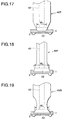
- Fig. 17 through Fig. 19 respectively show the sixth, seventh and eighth embodiments of the present invention.
- the point that chip junction nozzles 40E, 40F, and 40G respectively form opposite slant planes 43 which are symmetrical to the nozzle center axis P is the same as that in the first embodiment, however, the width of the chip junction nozzle viewed from the side surface is changed in the position of the height direction. According to this, the widths W1, W2, and W3 of the chip junction nozzles with which the edges of the chips come into contact, are respectively different, and impedance at the chip mounting viewed from the vibration apparatus which holds chip junction nozzle and generates ultrasonic, is changed, and impedance matching can be intended.
- the other structures are the same as those in the first embodiment, and the same or corresponding portion is denoted by the same code, and its explanation is omitted. That is, by changing the natural vibration frequency of the chip junction nozzle, the transmission of the vibration energy to the chip can be effectively conducted.
- the slope of the chip junction nozzle which is mirror finished is formed into a slope having very high hardness by the DLC processing, however, it is not limited to the DLC processing, but when the slope is a nozzle material having the hardness more than HrC40, or surface treated, the wear resistance, which is enough in practical use, can be assured.
- the surface roughness of the slope of the chip junction nozzle is made such that the center line average roughness is about 0.2 ⁇ m which is a very smooth mirror surface, however, when the surface roughness is made such that it is smoother than 1 rank as compared to the surface roughness when measured in Fig. 7 and Fig. 8, that is the center line average roughness is not more than 1.6 ⁇ m, the slope becomes practically mirror finishing, and the wear resistance between the edge of the chip and the slope can be enough reduced.
- the chip junction nozzle of the present invention when the chip is jointed onto the printed circuit board in the face down mounting of the chip, the chip can be jointed in the situation that the chip is always parallel to the pattern of the printed circuit board to be jointed, thereby, mounting with the uniform and strong junction strength can be carried out.
- This effect is effective for all the case where junction is carried out specifically by using the pressure as the junction element in mounting of the flip chip method, and the larger effect can be obtained when the ultrasonic is the junction element.
Applications Claiming Priority (2)
| Application Number | Priority Date | Filing Date | Title |
|---|---|---|---|
| JP37531498A JP3556498B2 (ja) | 1998-12-14 | 1998-12-14 | チップ接合用ノズル |
| JP37531498 | 1998-12-14 |
Publications (3)
| Publication Number | Publication Date |
|---|---|
| EP1011127A2 true EP1011127A2 (de) | 2000-06-21 |
| EP1011127A3 EP1011127A3 (de) | 2001-08-22 |
| EP1011127B1 EP1011127B1 (de) | 2006-10-18 |
Family
ID=18505319
Family Applications (1)
| Application Number | Title | Priority Date | Filing Date |
|---|---|---|---|
| EP99124956A Expired - Lifetime EP1011127B1 (de) | 1998-12-14 | 1999-12-14 | Chipverbindungsdüse |
Country Status (4)
| Country | Link |
|---|---|
| US (2) | US6189760B1 (de) |
| EP (1) | EP1011127B1 (de) |
| JP (1) | JP3556498B2 (de) |
| DE (1) | DE69933639T2 (de) |
Cited By (1)
| Publication number | Priority date | Publication date | Assignee | Title |
|---|---|---|---|---|
| EP1394839A2 (de) | 2002-08-29 | 2004-03-03 | Murata Manufacturing Co., Ltd. | Methode zum Ultraschallschweissen und entsprechende Vorrichtung |
Families Citing this family (14)
| Publication number | Priority date | Publication date | Assignee | Title |
|---|---|---|---|---|
| JP4469503B2 (ja) * | 1998-09-01 | 2010-05-26 | パナソニック株式会社 | バンプ接合判定装置及び方法、並びに半導体部品製造装置及び方法 |
| JP3556498B2 (ja) * | 1998-12-14 | 2004-08-18 | Tdk株式会社 | チップ接合用ノズル |
| US6885522B1 (en) * | 1999-05-28 | 2005-04-26 | Fujitsu Limited | Head assembly having integrated circuit chip covered by layer which prevents foreign particle generation |
| JP2003197686A (ja) * | 2001-10-18 | 2003-07-11 | Nec Corp | 電子部品実装装置及び電子部品実装方法 |
| JP2005159061A (ja) * | 2003-11-27 | 2005-06-16 | Fujitsu Ltd | 超音波ツール及び超音波接合装置 |
| JP4507941B2 (ja) * | 2005-03-28 | 2010-07-21 | パナソニック電工株式会社 | 超音波接合装置の製造方法 |
| US7868440B2 (en) * | 2006-08-25 | 2011-01-11 | Micron Technology, Inc. | Packaged microdevices and methods for manufacturing packaged microdevices |
| JP5237900B2 (ja) * | 2009-08-11 | 2013-07-17 | ルネサスエレクトロニクス株式会社 | 半導体装置の製造方法 |
| JP5890960B2 (ja) * | 2011-02-21 | 2016-03-22 | 積水化学工業株式会社 | フリップチップ実装方法 |
| JP5838637B2 (ja) * | 2011-08-02 | 2016-01-06 | 日産自動車株式会社 | 超音波溶接装置及び超音波溶接装置で使用される超音波接合工具のローレット面加工方法 |
| JP5741299B2 (ja) * | 2011-08-02 | 2015-07-01 | 日産自動車株式会社 | 超音波溶接工具のローレット面再加工方法 |
| US20140069989A1 (en) * | 2012-09-13 | 2014-03-13 | Texas Instruments Incorporated | Thin Semiconductor Chip Mounting |
| JP6201373B2 (ja) * | 2013-03-29 | 2017-09-27 | 日本電気株式会社 | 吸着コレット、ピックアップ装置、及びピックアップ方法 |
| JP6379447B2 (ja) * | 2013-04-16 | 2018-08-29 | 凸版印刷株式会社 | Icチップの実装方法 |
Citations (7)
| Publication number | Priority date | Publication date | Assignee | Title |
|---|---|---|---|---|
| US3575333A (en) * | 1968-11-21 | 1971-04-20 | Kulicke & Soffa Ind Inc | Beam-lead bonding apparatus |
| US3700155A (en) * | 1970-05-20 | 1972-10-24 | Mech El Ind Inc | Apparatus for improving alignment of beam leaded bonding tools |
| JPS59208844A (ja) * | 1983-05-13 | 1984-11-27 | Hitachi Ltd | フエイスダウンボンダ− |
| US4667870A (en) * | 1984-09-20 | 1987-05-26 | American Telephone And Telegraph Company | Registering articles to sites with recessed ultrasonic bonding tool head |
| JPH01244630A (ja) * | 1988-03-26 | 1989-09-29 | Nec Corp | 半導体ペレットのボンディング方法 |
| JPH04170035A (ja) * | 1990-11-02 | 1992-06-17 | Nec Yamagata Ltd | スクラブ用半導体チップ吸着ノズル |
| WO2001024963A1 (fr) * | 1999-10-04 | 2001-04-12 | Matsushita Electric Industrial Co., Ltd. | Technique et dispositif de raccordement far frottement et outil de maintien utilise avec le dispositifs de raccordement par friction |
Family Cites Families (6)
| Publication number | Priority date | Publication date | Assignee | Title |
|---|---|---|---|---|
| US4628584A (en) * | 1985-01-28 | 1986-12-16 | The Dow Chemical Company | Method of removing fibers protruding into bores |
| JPH04216641A (ja) | 1990-12-17 | 1992-08-06 | Nippon Telegr & Teleph Corp <Ntt> | リードボンディング装置用ステージ |
| JP2500778B2 (ja) | 1993-08-11 | 1996-05-29 | 日本電気株式会社 | ボンディングツ―ル及びボンディング方法 |
| JPH07115109A (ja) | 1993-10-15 | 1995-05-02 | Nec Corp | フリップチップボンディング方法及び装置 |
| EP0901152B1 (de) * | 1997-09-03 | 2003-04-02 | Nippon Pillar Packing Co., Ltd. | Träger für einen Halbleiterwafer mit einer CVD Siliziumkarbiden Filmbeschichtung |
| JP3556498B2 (ja) * | 1998-12-14 | 2004-08-18 | Tdk株式会社 | チップ接合用ノズル |
-
1998
- 1998-12-14 JP JP37531498A patent/JP3556498B2/ja not_active Expired - Fee Related
-
1999
- 1999-12-13 US US09/460,109 patent/US6189760B1/en not_active Expired - Fee Related
- 1999-12-14 DE DE69933639T patent/DE69933639T2/de not_active Expired - Fee Related
- 1999-12-14 EP EP99124956A patent/EP1011127B1/de not_active Expired - Lifetime
-
2001
- 2001-02-01 US US09/774,624 patent/US6382495B2/en not_active Expired - Fee Related
Patent Citations (7)
| Publication number | Priority date | Publication date | Assignee | Title |
|---|---|---|---|---|
| US3575333A (en) * | 1968-11-21 | 1971-04-20 | Kulicke & Soffa Ind Inc | Beam-lead bonding apparatus |
| US3700155A (en) * | 1970-05-20 | 1972-10-24 | Mech El Ind Inc | Apparatus for improving alignment of beam leaded bonding tools |
| JPS59208844A (ja) * | 1983-05-13 | 1984-11-27 | Hitachi Ltd | フエイスダウンボンダ− |
| US4667870A (en) * | 1984-09-20 | 1987-05-26 | American Telephone And Telegraph Company | Registering articles to sites with recessed ultrasonic bonding tool head |
| JPH01244630A (ja) * | 1988-03-26 | 1989-09-29 | Nec Corp | 半導体ペレットのボンディング方法 |
| JPH04170035A (ja) * | 1990-11-02 | 1992-06-17 | Nec Yamagata Ltd | スクラブ用半導体チップ吸着ノズル |
| WO2001024963A1 (fr) * | 1999-10-04 | 2001-04-12 | Matsushita Electric Industrial Co., Ltd. | Technique et dispositif de raccordement far frottement et outil de maintien utilise avec le dispositifs de raccordement par friction |
Non-Patent Citations (3)
| Title |
|---|
| PATENT ABSTRACTS OF JAPAN vol. 009, no. 069 (E-305), 29 March 1985 (1985-03-29) & JP 59 208844 A (HITACHI SEISAKUSHO KK), 27 November 1984 (1984-11-27) * |
| PATENT ABSTRACTS OF JAPAN vol. 013, no. 581 (E-865), 21 December 1989 (1989-12-21) -& JP 01 244630 A (NEC CORP), 29 September 1989 (1989-09-29) * |
| PATENT ABSTRACTS OF JAPAN vol. 016, no. 472 (E-1272), 30 September 1992 (1992-09-30) -& JP 04 170035 A (NEC YAMAGATA LTD), 17 June 1992 (1992-06-17) * |
Cited By (3)
| Publication number | Priority date | Publication date | Assignee | Title |
|---|---|---|---|---|
| EP1394839A2 (de) | 2002-08-29 | 2004-03-03 | Murata Manufacturing Co., Ltd. | Methode zum Ultraschallschweissen und entsprechende Vorrichtung |
| EP1394839A3 (de) * | 2002-08-29 | 2005-08-17 | Murata Manufacturing Co., Ltd. | Methode zum Ultraschallschweissen und entsprechende Vorrichtung |
| US7017791B2 (en) | 2002-08-29 | 2006-03-28 | Murata Manufacturing Co., Ltd. | Ultrasonic bonding method and device |
Also Published As
| Publication number | Publication date |
|---|---|
| JP3556498B2 (ja) | 2004-08-18 |
| US20010011668A1 (en) | 2001-08-09 |
| US6382495B2 (en) | 2002-05-07 |
| DE69933639T2 (de) | 2007-03-01 |
| EP1011127A3 (de) | 2001-08-22 |
| JP2000183115A (ja) | 2000-06-30 |
| DE69933639D1 (de) | 2006-11-30 |
| US6189760B1 (en) | 2001-02-20 |
| EP1011127B1 (de) | 2006-10-18 |
Similar Documents
| Publication | Publication Date | Title |
|---|---|---|
| EP1011127B1 (de) | Chipverbindungsdüse | |
| US6056191A (en) | Method and apparatus for forming solder bumps | |
| US10864597B2 (en) | Ultrasonic bonding tool, method for manufacturing ultrasonic bonding tool, ultrasonic bonding method, and ultrasonic bonding apparatus | |
| US7549567B2 (en) | Component mounting tool, and method and apparatus for mounting component using this tool | |
| US20080265002A1 (en) | Method of ultrasonic mounting and ultrasonic mounting apparatus using the same | |
| US20050003636A1 (en) | Manufacturing method of semiconductor device | |
| US5687901A (en) | Process and apparatus for forming ball bumps | |
| US6686225B2 (en) | Method of separating semiconductor dies from a wafer | |
| EP0787820A3 (de) | Methoden zum Vorbereiten von Schneidwerkzeug-Grundkörper zur Beschichtung mit Diamant, sowie dadurch erhaltene Produkte | |
| KR20070113109A (ko) | 반도체장치의 제조방법 | |
| US6706130B1 (en) | Method and device for frictional connection and holding tool used for the frictional connection device | |
| US20060065697A1 (en) | Bonding tool for ultrasonic bonding and method of ultrasonic bonding | |
| US20030020142A1 (en) | Semiconductor die with contoured bottom surface and method for making same | |
| CN1312764C (zh) | 电子元件装置及其制造方法 | |
| US7037753B2 (en) | Non-planar surface for semiconductor chips | |
| EP1137061B1 (de) | Arbeitsmethode und vorrichtung | |
| JP2004165536A (ja) | フリップチップ接合方法およびその装置 | |
| JP4337336B2 (ja) | インクジェット記録ヘッド及びその製造方法 | |
| JP4223164B2 (ja) | バンプ付電子部品のボンディング方法及びボンディング装置 | |
| JPH1140646A (ja) | ピックアップツール | |
| JP2004136634A (ja) | インクジェットヘッドおよびその製造方法 | |
| JP5967545B2 (ja) | 電子部品ボンディングツール | |
| CN115669239A (zh) | 基于形貌的沉积高度调节 | |
| KR20190084650A (ko) | 미리 정해진 패턴으로 분포된 다수의 수용부에 솔더볼을 안착시키는 솔더볼 처리 장치 | |
| JPH03215950A (ja) | アウタリードボンダ |
Legal Events
| Date | Code | Title | Description |
|---|---|---|---|
| PUAI | Public reference made under article 153(3) epc to a published international application that has entered the european phase |
Free format text: ORIGINAL CODE: 0009012 |
|
| AK | Designated contracting states |
Kind code of ref document: A2 Designated state(s): AT BE CH CY DE DK ES FI FR GB GR IE IT LI LU MC NL PT SE |
|
| AX | Request for extension of the european patent |
Free format text: AL;LT;LV;MK;RO;SI |
|
| PUAL | Search report despatched |
Free format text: ORIGINAL CODE: 0009013 |
|
| AK | Designated contracting states |
Kind code of ref document: A3 Designated state(s): AT BE CH CY DE DK ES FI FR GB GR IE IT LI LU MC NL PT SE |
|
| AX | Request for extension of the european patent |
Free format text: AL;LT;LV;MK;RO;SI |
|
| 17P | Request for examination filed |
Effective date: 20011025 |
|
| AKX | Designation fees paid |
Free format text: DE FR GB |
|
| GRAP | Despatch of communication of intention to grant a patent |
Free format text: ORIGINAL CODE: EPIDOSNIGR1 |
|
| GRAS | Grant fee paid |
Free format text: ORIGINAL CODE: EPIDOSNIGR3 |
|
| GRAA | (expected) grant |
Free format text: ORIGINAL CODE: 0009210 |
|
| AK | Designated contracting states |
Kind code of ref document: B1 Designated state(s): DE FR GB |
|
| REG | Reference to a national code |
Ref country code: GB Ref legal event code: FG4D |
|
| REF | Corresponds to: |
Ref document number: 69933639 Country of ref document: DE Date of ref document: 20061130 Kind code of ref document: P |
|
| ET | Fr: translation filed | ||
| PLBE | No opposition filed within time limit |
Free format text: ORIGINAL CODE: 0009261 |
|
| STAA | Information on the status of an ep patent application or granted ep patent |
Free format text: STATUS: NO OPPOSITION FILED WITHIN TIME LIMIT |
|
| 26N | No opposition filed |
Effective date: 20070719 |
|
| PGFP | Annual fee paid to national office [announced via postgrant information from national office to epo] |
Ref country code: FR Payment date: 20081212 Year of fee payment: 10 |
|
| PGFP | Annual fee paid to national office [announced via postgrant information from national office to epo] |
Ref country code: DE Payment date: 20081211 Year of fee payment: 10 |
|
| PGFP | Annual fee paid to national office [announced via postgrant information from national office to epo] |
Ref country code: GB Payment date: 20081210 Year of fee payment: 10 |
|
| GBPC | Gb: european patent ceased through non-payment of renewal fee |
Effective date: 20091214 |
|
| REG | Reference to a national code |
Ref country code: FR Ref legal event code: ST Effective date: 20100831 |
|
| PG25 | Lapsed in a contracting state [announced via postgrant information from national office to epo] |
Ref country code: FR Free format text: LAPSE BECAUSE OF NON-PAYMENT OF DUE FEES Effective date: 20091231 |
|
| PG25 | Lapsed in a contracting state [announced via postgrant information from national office to epo] |
Ref country code: DE Free format text: LAPSE BECAUSE OF NON-PAYMENT OF DUE FEES Effective date: 20100701 |
|
| PG25 | Lapsed in a contracting state [announced via postgrant information from national office to epo] |
Ref country code: GB Free format text: LAPSE BECAUSE OF NON-PAYMENT OF DUE FEES Effective date: 20091214 |