EP0987822A2 - Circuit PLL avec oscillateur en anneau et méthode de côntrole - Google Patents
Circuit PLL avec oscillateur en anneau et méthode de côntrole Download PDFInfo
- Publication number
- EP0987822A2 EP0987822A2 EP99116166A EP99116166A EP0987822A2 EP 0987822 A2 EP0987822 A2 EP 0987822A2 EP 99116166 A EP99116166 A EP 99116166A EP 99116166 A EP99116166 A EP 99116166A EP 0987822 A2 EP0987822 A2 EP 0987822A2
- Authority
- EP
- European Patent Office
- Prior art keywords
- oscillation
- signal
- oscillator
- differential amplifier
- circuit
- Prior art date
- Legal status (The legal status is an assumption and is not a legal conclusion. Google has not performed a legal analysis and makes no representation as to the accuracy of the status listed.)
- Withdrawn
Links
- 238000000034 method Methods 0.000 title description 6
- 230000010355 oscillation Effects 0.000 claims abstract description 219
- 238000001514 detection method Methods 0.000 claims description 8
- 238000012544 monitoring process Methods 0.000 description 31
- 238000010586 diagram Methods 0.000 description 14
- 238000013459 approach Methods 0.000 description 5
- 239000000872 buffer Substances 0.000 description 3
- 230000003111 delayed effect Effects 0.000 description 3
- 230000005684 electric field Effects 0.000 description 3
- 230000000630 rising effect Effects 0.000 description 3
- 230000015572 biosynthetic process Effects 0.000 description 1
- 238000004891 communication Methods 0.000 description 1
- 238000007796 conventional method Methods 0.000 description 1
- 238000013461 design Methods 0.000 description 1
- 230000000694 effects Effects 0.000 description 1
- 230000000717 retained effect Effects 0.000 description 1
Images


Classifications
-
- H—ELECTRICITY
- H03—ELECTRONIC CIRCUITRY
- H03L—AUTOMATIC CONTROL, STARTING, SYNCHRONISATION OR STABILISATION OF GENERATORS OF ELECTRONIC OSCILLATIONS OR PULSES
- H03L7/00—Automatic control of frequency or phase; Synchronisation
- H03L7/06—Automatic control of frequency or phase; Synchronisation using a reference signal applied to a frequency- or phase-locked loop
- H03L7/08—Details of the phase-locked loop
- H03L7/083—Details of the phase-locked loop the reference signal being additionally directly applied to the generator
-
- H—ELECTRICITY
- H03—ELECTRONIC CIRCUITRY
- H03K—PULSE TECHNIQUE
- H03K3/00—Circuits for generating electric pulses; Monostable, bistable or multistable circuits
- H03K3/02—Generators characterised by the type of circuit or by the means used for producing pulses
- H03K3/023—Generators characterised by the type of circuit or by the means used for producing pulses by the use of differential amplifiers or comparators, with internal or external positive feedback
- H03K3/0231—Astable circuits
-
- H—ELECTRICITY
- H03—ELECTRONIC CIRCUITRY
- H03K—PULSE TECHNIQUE
- H03K3/00—Circuits for generating electric pulses; Monostable, bistable or multistable circuits
- H03K3/02—Generators characterised by the type of circuit or by the means used for producing pulses
- H03K3/027—Generators characterised by the type of circuit or by the means used for producing pulses by the use of logic circuits, with internal or external positive feedback
- H03K3/03—Astable circuits
- H03K3/0315—Ring oscillators
- H03K3/0322—Ring oscillators with differential cells
-
- H—ELECTRICITY
- H03—ELECTRONIC CIRCUITRY
- H03L—AUTOMATIC CONTROL, STARTING, SYNCHRONISATION OR STABILISATION OF GENERATORS OF ELECTRONIC OSCILLATIONS OR PULSES
- H03L3/00—Starting of generators
-
- H—ELECTRICITY
- H03—ELECTRONIC CIRCUITRY
- H03L—AUTOMATIC CONTROL, STARTING, SYNCHRONISATION OR STABILISATION OF GENERATORS OF ELECTRONIC OSCILLATIONS OR PULSES
- H03L7/00—Automatic control of frequency or phase; Synchronisation
- H03L7/06—Automatic control of frequency or phase; Synchronisation using a reference signal applied to a frequency- or phase-locked loop
- H03L7/08—Details of the phase-locked loop
- H03L7/099—Details of the phase-locked loop concerning mainly the controlled oscillator of the loop
- H03L7/0995—Details of the phase-locked loop concerning mainly the controlled oscillator of the loop the oscillator comprising a ring oscillator
Definitions
- This invention relates to a PLL (Phase-locked loop) circuit and a method of controlling the same, and in particular, to a PLL circuit which is capable of automatically restoring to a normal state when an oscillation operation is halted on the condition that an oscillation state of a voltage oscillation circuit (VCO) is monitored.
- VCO voltage oscillation circuit
- phase clocks are generally designed among the phase clocks of the Nth power of 2 in the system.
- the first conventional reference discloses a clock generator which has a ring oscillator including odd stages of delay circuits and which directly and separately produces output signals of a plurality of the delay circuits as clock signals of multi-phase.
- the system can not produce phase clocks of the Nth power of 2.
- the second conventional reference discloses a clock generator which has four phase detectors for detecting phase modulation signals of eight phase and which produce clock signals of eight phases by giving output signals of a voltage control oscillator for producing a single phase clock into the phase detector.
- This system can produce the phase clocks (eight phase clocks) of Nth power of 2.
- operation speed of the detector is restricted. In consequence, the system can not produce high-speed clocks. Further, it is difficult in design to unify delay times of the four detectors.
- the third reference discloses an oscillator of multi-phase to which buffers are connected in series with a plurality of stages. With this structure, an output signal of the final stage is reversed, and is fed back into the first stage of the buffer.
- the each of the buffers is composed of two inverters.
- the ring oscillator of the voltage control oscillator is structured by even devices.
- the oscillation operation may be halted by an affect of noise when a power supply is introduced.
- even differential amplifiers 81 through 84 are connected in series, and an input of first stage and an output of final stage are connected in a ring form.
- all outputs of the differential amplifier are put into unbalanced states. For example, when an output 803 is put into a high level, an output 804 is put into a low level.
- the number of detachable devices is increased. Consequently, the number of device having no reset signal (power-on reset signal) when the power supply is introduced is also increased.
- the conventional device has the reset signal.
- the device can not make an initial value of the PLL circuit.
- a technique, in which the system monitors the output of the PLL circuit and the system is automatically restored to the normal state when the oscillation operation is halted, has been researched.
- a circuit illustrated in Fig. 2 includes a phase comparing circuit 91, a voltage generating circuit 92, a voltage control oscillator 93, and a self-restoring control circuit 94.
- the phase comparing circuit 91 compares a referential signal 901 with an oscillation signal 904 and produces a phase difference detecting signal 902.
- the voltage generating circuit 92 converts the phase difference detecting signal 902 into a voltage 903.
- the voltage control oscillator 93 produces a frequency signal proportional to the voltage 903.
- the self-restoring control circuit 94 monitors the referential signal 901 and the oscillation signal 904, and supplies a self-restoring signal 905 into the phase comparing circuit 91.
- the phase comparing circuit 91 gives the phase difference detecting signal 902 into the voltage generating circuit 92 on the basis of the self-restoring signal 905 given from the self-restoring control circuit 94 at a constant duration after the voltage control oscillator 93 halts. Thereby, the system is self-restored to the normal oscillation state.
- the voltage control oscillator having even stages of ring oscillator may halt the oscillation even when the voltage from the voltage generating circuit is normal. However, the system can not be automatically restored from this state.
- the voltage control oscillator having odd stages of ring oscillator inevitably and normally oscillates when the voltage from the voltage generating circuit is normal.
- the oscillation halts only when the voltage approaches a ground line GND level or a power supply line VDD level.
- the self-restoring signal is given to the voltage generating circuit, and an output voltage of the voltage generating circuit is put into a normal value.
- the self-restoring control is carried out.
- oscillation frequency is variable proportional to a control voltage from the voltage generating circuit in the ring oscillator.
- the control voltage approaches the power supply line VDD level or the ground line GND level, the ring oscillator does not become the normal oscillation state, and the oscillation inevitably halts.
- a drain of a transistor 705 is connected to a drain of a transistor 752. Further, drains of the transistors 751 and 753 are connected to each other. Sources of transistors 750 and 751 are coupled to a power supply line VDD. Sources of transistors 752 and 753 are connected to a drain of a transistor 754. A source of a transistor 754 is coupled to a ground line GND of a transistor 754.
- a gate of a transistor 750 is connected to a gate of a transistor 751 to form control input terminal 701 from an external circuit.
- a gate of a transistor 754 serves as an control input 704 from an external circuit.
- Each of gates 702 and 703 of transistors 752 and 753 serves as an input terminal while each of drains 706 and 705 of transistors 752 and 753 serves as an output terminal.
- the transistor 752 When a high level is given to the input terminal 702 and a low level is given to the input terminal 703, the transistor 752 is put into an ON state, the output 706 is put into the low level, the transistor 753 is put into an OFF state, and the output 705 is put into the high level.
- the voltage 903 from the voltage generating circuit 92 is applied to the control inputs 701 and 704 of the transistors 750, 751, and 754, and the delay time of the differential amplifier is variable in dependency upon the voltage. By utilizing this phenomenon, the oscillation frequency of the ring oscillator is changed.
- each of the transistors 750, 751 and 754 is put into the OFF state, and no current flows.
- the circuit can not be operable as the differential amplifier, and as a result, the oscillation inevitably halts.
- JP-A-55-42443 JP-A-63-185121, JP-A-5-122032, JP-A-8-79068, JP-A-8-307460, and JP-A-9-326692.
- PLL Phase-looked loop
- a PLL circuit detects oscillation halt of a voltage control oscillator, generates an oscillation control signal for automatically oscillating the voltage control oscillator based upon the detected signal, and automatically restores the voltage control oscillator to a normal oscillation state by the use of the generated signal.
- the voltage control oscillator is structured by a ring oscillator in which a plurality of differential amplifiers are connected in a ring form.
- a plurality of oscillation control means are arranged for the respective inputs of the differential amplifiers so as to set the ring oscillator into an oscillationable state when the voltage control oscillator halts.
- the oscillation control means is controlled by the oscillating control signal.
- the number of the differential amplifiers is even.
- the oscillation control means pulls-up one input of the differential amplifier into a high level and pulls-down the other input of the differential amplifier into a low level.
- the oscillation control means comprises a first oscillation control means which pulls-up the one input of the differential amplifier into the high level and a second oscillation control means which pulls-down the other input of the differential amplifier into the low level.
- the first oscillation control means comprises a p-channel transistor which is connected between the one input of the differential amplifier and a power supply line.
- the second oscillation control means comprises an n-channel transistor which is connected between the other input of the differential amplifier and a ground line.
- the circuit has second and third differential amplifiers.
- one output of the differential amplifier constituting the ring oscillator is introduced to a non-reverse input terminal of the second differential amplifier while the other output of the differential amplifier is introduced to a reverse input terminal of the second differential amplifier.
- one output of the differential amplifier constituting the ring oscillator is introduced to a reverse input terminal of the third differential amplifier while the other output of the differential amplifier is introduced to a non-reverse input terminal of the third differential amplifier.
- a plurality of frequencies are generated.
- Each of the frequency has a predetermined phase difference for the ring oscillator.
- the circuit has a detection circuit which detects the oscillation halt of the voltage control oscillator.
- the detection circuit comprises a divider, a first data retaining means, a second date retaining means, an exclusive OR gate.
- the divider divides the oscillation signal of the voltage control oscillator
- the first data retaining means retains a first output signal which is given from the divider at a first time while the second data retaining means retains a second output signal which is given from the divider at a second time after a predetermined time from the first time.
- the exclusive OR gate detects the presence or absence of difference between the first output signal and the second output signal.
- Each of the first data retaining means and the second data retaining means is reset by the use of the oscillation control signal.
- the circuit has a detection circuit which detects the oscillation halt of the voltage control oscillator.
- the detection circuit comprises a divider, a plurality of shift registers, and an exclusive OR gate.
- the divider divides the oscillation signal of the voltage control oscillator.
- a plurality of shift registers sequentially shift the divided signals.
- the exclusive OR gate detects the presence or absence of difference between an input signal and an output signal of each shift register. Each of the shift registers is reset by the use of the oscillation control signal.
- the ring oscillator portion is composed of even stages differential amplifiers. Consequently, the multi-phase clocks of N power of 2 can be produced with a simple circuit.
- the oscillation monitoring circuit always monitors the oscillation state of the PLL circuit, and gives the reset signal into the voltage control oscillator so as to be oscillationable state using the oscillation halt as a trigger when the oscillation monitoring circuit detects the oscillation halt. In consequence, when the oscillation of the PLL circuit halts, the PLL circuit can be automatically restored.
- the ring oscillator of the voltage control oscillator is directly reset into the oscillation state. Consequently, when the oscillation of the PLL circuit halts, the PLL circuit can accurately return into the oscillation state.
- a PLL (Phase-locked loop) circuit detects halt of an oscillation of a voltage control oscillator 30, generates an oscillation control signal 107 for automatically oscillating the voltage control oscillator on the basis of the detected signal, and restores the voltage control oscillator 30 to a normal state by the use of the signal 107.
- the voltage control oscillator 30 is structured by a ring oscillator in which a plurality of differential amplifiers 32 through 35 are connected in a ring form and oscillation control means P1 - P4 and N1 - N4 is provided for each input of each differential amplifier 32 - 35.
- the oscillation control means sets the ring oscillator into an oscillationable state when the oscillation of the voltage control oscillator 30 halts. In this event, the oscillation control means P1 - P4 and N1 - N4 is controlled by the oscillation control signal 107.
- the number of the differential amplifiers is even. Further, one input of the differential amplifier is pulled-up to a high level while the other input of the differential amplifier is pulled-down to a low level.
- a second differential amplifier 411 there are provided with a second differential amplifier 411 and a third differential amplifier 415.
- One output of a differential amplifier 401 constituting the ring oscillator is coupled to a non-reverse input terminal (+) of the second differential amplifier 411 while the other output of the differential amplifier 401 is coupled to a reverse input terminal (-) of the second differential amplifier 411.
- one output of a differential amplifier constituting the ring oscillator is coupled to a non-reverse terminal (-) of the third differential amplifier 495 while the other output of the differential amplifier 401 is coupled to non-reverse input terminal (+) of the third differential amplifier 495.
- an oscillation monitoring circuit 50 for detecting the oscillation halt of the voltage control oscillator 30 includes a divider 51 (402), a first data retaining means 52 (404), a second data retaining means 53 (405), and an exclusive-OR gate 59 (406).
- the divider 51 (402) divides an oscillation signal 105 of the voltage control oscillator 30.
- the first data retaining means 52 (404) retains a first output signal 502 (454) at a first time outputted from the divider 51 (402).
- the second data retaining means 51 (402) retains a second output signal 503 (454) outputted from the divider 51 (402) at a second time after a predetermined time from the first time.
- the exclusive-OR gate 59 (406) detects the presence or absence of difference between the first output signal 502 and the second output signal 503.
- the first data retaining means 52 (404) and the second data retaining means 53 (405) are reset by the oscillation control signal 107 in the PLL circuit.
- the oscillation control oscillator 50 includes a divider 51, a plurality of shift registers 52 - 55, exclusive-OR gates 56 - 58.
- the divider 51 divides an oscillation signal 105 of the voltage control oscillator 30.
- the shift registers 52 - 55 sequentially shift the signals divided by the divider 51.
- the exclusive-OR gates 56 - 58 detect the presence or absence of difference between an input signal and an output signal of each shift register 52 - 55. In this event, the shift registers 52 - 55 are rest by the oscillation control signal 107 in the PLL circuit.
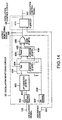
- a PLL circuit includes a PLL oscillator 1, which is composed of a divider 40, a phase comparing circuit 10, a voltage generating circuit 20 and a voltage control oscillator 30, an oscillator monitoring circuit 50, and an oscillator control circuit 60.
- the divider 40 divides an oscillating signal 105 into N number.
- the phase comparing circuit 10 compares the phase between the divided signal 104 and a referential signal 101 and produces a phase difference signal 102.
- the voltage generating circuit 20 converts the phase difference signal 102 into a voltage.
- the voltage control oscillator 30 changes an oscillation frequency proportional to the voltage 103.
- the oscillation monitoring circuit 50 monitors an oscillation state of the oscillation signal 105 of the PLL oscillator 1 and produces the presence or absence of the oscillation as an monitoring signal 106.
- the oscillation control circuit 60 produces an oscillation control signal 107 for controlling the voltage control oscillation circuit 30 by the use of the monitoring signal 106.
- phase comparing circuit 10 With respect to the phase comparing circuit 10, the voltage generating circuit 20 and the divider 40, the detail structure will be omitted because they are well known in the art.
- a ring oscillator is used as an oscillation portion of the voltage control oscillator 30.
- the structure except the oscillation portion has been well known in the art. Therefore, the specific structure will be omitted.
- the ring oscillator is structured in a ring form.
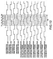
- the oscillation frequency depends upon only delay time of the differential amplifiers 401, 402, 403 and 404.
- a voltage comparator 411 compares a positive output 451 and a negative output 452 as outputs of the differential amplifier 401 in level. As a result of the comparison, when the level of the positive phase 451 is higher, the voltage comparator 411 produces a high level to an output 491. When the level is not higher, the voltage comparator 411 produces a low level.
- Each of the voltage comparators 412 - 418 is structured in the same manner.
- a plus input of the voltage comparator 415 is coupled to the negative output 452 of the differential amplifier 401 while the minus input is coupled to the positive output 451.
- Outputs of the differential amplifiers 402 - 404 are coupled to the voltage comparators 412, 416, 413, 417, 414 and 418 so as to produce outputs 491 - 498.
- the ring oscillator composed of four stages differential amplifiers may be structure in the same manner.
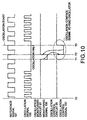
- ring oscillator In the ring oscillator illustrated in Fig. 6, even number of differential amplifiers 32 - 35 are connected in series. With this structure, a positive input of a first stage is coupled to a negative output of a final stage while a negative output of the first stage is coupled to a positive output of the final stage.
- the ring oscillator is structured in a ring form. Under this circumstance, oscillation frequency depends upon delay time of the differential amplifier.
- Each of P-type electric field transistors P1 - P4 and N-type electric field transistors N1 - N4 serves as a control device for self-restoring the oscillator, and is connected to each of output terminals 302 - 309 of the differential amplifiers 32 - 35.
- a drain is coupled to a positive output 302 of the differential amplifier 32 while a source is connected to a power supply line VDD.
- a drain is coupled to a negative output 303 of the differential amplifier 32 while a source is coupled to a ground line GND.
- Transistors P2 - P4 and N2 - N4 are connected to the differential amplifiers 33 - 35 in the same manner.
- Each gate of the transistors N1 - N4 is given with a signal ,which is reversed the oscillation control signal 107, from the oscillation control circuit 60 illustrated in Fig. 4 by a reverse gate 31.
- each gate of the transistors P1 - P4 is given with the oscillation control signal 107.
- Each of the transistors P1 - P4 and N1 - N4 is turned off when the oscillation control signal 107 becomes the high level, and is turned on when the signal 107 becomes the low level.
- the ring oscillator composed of four stages differential amplifiers may be structured in the same manner.
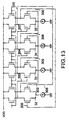
- the differential amplifier includes a differential amplifier portion which is composed of P-type transistors 750, 751 and N-type transistors 752, 753, a P-type transistor 755 which is connected to the P-type transistor 750 in parallel, a P-type transistor 756 which is connected to the P-type transistor 751 in parallel, and an N-type transistor 757 which is connected to the N-type transistor 754.
- a drain of the transistor 750 is coupled to a drain of the transistor 752
- a drain of the transistor 751 is coupled to a drain of the transistor 753 and each source of the transistors 750, 751 is connected to the power supply line VDD.
- each source of the transistors 752, 753 is coupled to a drain of the transistor 754, and a source of the transistor 754 is coupled to the ground line GND.
- a gate of the transistor 750 is connected to a gate of the transistor 751 so as to constitute a control input terminal 701 from an external.
- a gate of the transistor 754 also serves as a control input terminal 704 from the external.
- Input terminals of the differential amplifier serve as gates 702, 703 of the transistors 752, 753 while output terminals serve as drains 706, 705 of the transistors 752, 753.
- a gate of the transistor 755 is connected to a gate of the transistor 756 so as to constitute a control input terminal 707 from the external.
- a gate of the transistor 757 also constitutes a control input terminal 708 from the external.
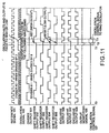
- the oscillation monitoring circuit 50 illustrated in Fig. 8 always monitors whether or not the PLL oscillator oscillates and produces the monitor signal which indicates the oscillation state.
- the oscillation monitoring circuit 50 includes a divider 51, shift-registers 52-55, exclusive OR-gates 56 - 58, and an OR-gate 59, as illustrated in Fig. 8.
- the divider 51 divides the oscillation signal 105 into the M number, and supplies the divided signal 501 into the shift register 52.
- the shift register retains a level of an input 501 at a timing in which the referential signal 101 is changed from the low level into the high level, and produces as a signal 502.
- each shift-register 53 - 55 An operation of each shift-register 53 - 55 is carried out in the same manner. Namely, the shift register 53 retains a level of a signal 502 at timing in which the referential signal 101 is changed from the low level into the high level, and produces as a signal 503.
- the shift register 54 shifts a signal 503 at a timing of the referential signal 101 and produces a signal 504 while the shift register 55 shifts a signal 504 to produce a signal 505.
- the oscillation control signal 107 is given into a set terminal SB of the shift register 52 and reset terminals RB of the shift registers 53 - 55. Under this circumstance, when the oscillation control signal 107 is put into the low level, an output of the shift register 52 is put into the high level, and each output of the shift registers 53 - 55 is put into the low level.
- each of the shifts registers 52 - 55 normally operate.
- the exclusive OR gate 56 produces the low level as the output signal 506 when both signals 502, 503 are equal to the high levels or the low levels.
- the exclusive OR-gate 57 which is given with signals 503, 504 and the exclusive OR-gate 58 which is given with signals 504, 505 operate in the same manner.
- the OR gate 59 produces the low level as the monitor signal 106 when all of signal 506 - 508 are equal to the low levels. That is, the low level is produced as the monitor signal 106 when all of output signals 502 - 505 are put into the high levels or the low levels.
- the oscillation control circuit 60 illustrated in Fig. 9 produces a pulse signal so that the voltage control oscillator 30 can resume the oscillation when an oscillation-halting signal is given thereto.
- the oscillation control circuit 60 is composed of a D flip-flop 61.
- the D flip-flop produces and retains the level of the monitor signal 106, which is given when the referential signal 101 is changed from the high level into the low level, as the oscillation control signal 107.
- the oscillation monitoring circuit 50 produces the monitor signal, which indicates the oscillation state, into the oscillation control circuit 60. In this case, the oscillation control circuit does not produce the oscillation control signal 107.
- the oscillation monitoring circuit 50 produces the monitor signal 106 of the low level, which indicates the halt of the oscillation, into the oscillation control circuit 60. Further, the oscillation control circuit 60 produces the oscillation control signal 107 into the voltage control oscillator 30 on the basis of the monitoring signal 106, resets the voltage control oscillator 30 into the oscillation state, and automatically restores the oscillation of the PLL circuit 1.
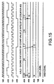
- the oscillation monitoring circuit 50 monitors the oscillation signal 105 of the PLL oscillator 1 in time T0 - T1, and puts the monitor signal 106 into the high level, which indicates the oscillation state, because the PLL oscillator 1 is in the oscillation state. Further, the oscillation control signal 107 as the output of the oscillation control circuit 60 is also put into the high level, and the voltage control oscillator 30 is particularly controlled.
- the oscillation monitoring circuit 50 detects the oscillation halt of the oscillation signal 105, the oscillation monitoring circuit 50 puts the monitoring signal into the low level which indicates the oscillation halt.
- the monitor signal 106 becomes the low level at falling time T2 of the referential signal 101. Consequently, the oscillation control circuit 60 puts the oscillation control signal into the low level, resets the shift register of the oscillation monitoring circuit 50, and puts the monitor signal 106 into the high level at falling time T3 of the referential signal 101.
- each differential amplifier of the ring oscillator of the voltage control circuit 30 is reset into the oscillationable state, and starts the normal oscillation.
- the oscillation monitoring circuit 50 monitors the oscillation signal 105 of the PLL oscillator 1 in time T0 - T1, and puts the monitor signal 106, which indicates the oscillation state, into the high level. Further, the oscillation monitoring circuit 50 puts The oscillation control signal 107 as the output of the oscillation control circuit 60 into the high level, and does not particularly control the voltage control oscillator 30.
- time T1 when the oscillation monitor circuit 50 detects the oscillation halt of the oscillation signal 105, the oscillation monitoring circuit 50 puts the monitor signal 106 into the low level which indicates the oscillation halt.
- the monitor signal 106 becomes the low level at falling time of the referential signal 101. Consequently, the oscillation control circuit 60 puts the oscillation control signal 107 into the low level, resets the shift register of the oscillation monitoring circuit 50, and puts the monitor signal 106 into the high level at falling time T3 of the referential signal 101.
- the oscillation control signal 107 becomes the low level. Thereby, each differential amplifier of the ring oscillator of the voltage control oscillator circuit 30 is reset into the oscillationable state, and the normal oscillation starts.
- the oscillation signal 105 which is given to the oscillation monitoring circuit 50, is divided by the divider 51 (eight division number in Fig. 11), and is supplied to the shift register 52.
- Each of shift registers 52 - 55 operates in synchronism with the rising of the referential signal 101, and the input data shifts in the direction from the shift register 52 into the shift register 55 at every rising of the referential signal 101.
- the D flip-flop 61 of the oscillation control circuit 60 continues so as to produce the high level into the oscillation control signal 107 because the monitor signal 106 is put into the high level.
- the oscillation control signal 107 is coupled to the set terminal and the reset terminal of the shift registers 52 - 55 of the oscillation monitoring circuit 50. In this event, each of the shift registers 52 - 55 is not set into the reset state and carries out the normal operation because the oscillation control signal 107 is put into the high level.
- the P-type transistors P1 - P4 each of which is given with the high level signal 107 and the N-type transistors N1 - N4, each of which is given with the low level signal 301 via the reverse gate 31, are put into OFF states not to be connected to the transistors.
- the normal ring oscillator is structured so as to perform the oscillation.
- the D flip-flop 61 of the oscillation control circuit 60 which is given with the output monitor signal 106 of the low level, puts the oscillation control signal 107 into the low level at falling time T2 of the referential signal 101.
- the shift register 52 is set, the output of the shift register 52 is put into the high level, the shift registers 53 - 55 are reset, and the output of the shift registers 53 - 55 are put into the low level because the oscillation control signal 107 becomes the low level. Further, the exclusive OR-gate 56 becomes the high level, and the monitor signal 106 of the OR-gate 59 is also changed from the low level into the high level.
- the P-type transistors P1 - P4 each of which is given with the low level signal 107 and the N-type transistors N1 - N4, each of which is given the high level signal 301 by the reverse gate 31, are put into the ON state.
- the monitor signal 106 is put into the high level at time T3 in which the referential signal subsequently falls. Consequently, the oscillation control signal is changed from the low level into the high level.
- the P-type transistors P1 - P4 each of which is given with the oscillation control signal 107 of the high level and the N-type transistors N1 - N4, each of which is given with the low-level signal by the reverse gate 31, become the OFF state.
- each potential of outputs 302 - 309 of the differential amplifiers 32 - 25 is changed from the power supply line VDD level or the ground line GND level into the intermediate potential level direction, and becomes the oscillation state in the course.
- the oscillation monitoring circuit 50 detects the oscillation halt, and puts the monitor signal 106 into the low level or puts the oscillation control signal 107 into the low level to be able to automatically restore the oscillation.
- the ring oscillator oscillates at oscillation frequency T0.
- the positive phase output 451 of the differential amplifier 401 is put into the high level while the negative phase output 452 is put into the low level. Consequently, the output 491 of the voltage comparator 411 becomes the high level while the output 495 of the voltage comparator 415 becomes the low level.
- the output of the differential amplifier 401 is reversed. In consequence, the output 491 of the voltage comparator 411 is put into the low level while the output 495 of the voltage comparator 415 is put into the high level.
- the positive phase output 451 of the differential amplifier 401 is changed from the low level into the high level while the negative phase output 452 is changed from the high level into the low level.
- the input of the next stage differential amplifier 402 is changed.
- the output 492 of the voltage comparator 412 is changed into the high level while the output 496 of the voltage comparator 416 is changed into the low level.
- the positive phase output 451 of the differential amplifier 401 is changed from the high level into the low level while the negative phase output 452 is changed from the low level into the high level.
- the input of the next stage differential amplifier 402 is changed.
- the output 492 of the voltage comparator 412 is changed into the low level while the output 496 of the voltage comparator 416 is changed into the high level.
- waveform delayed with delay time of the differential amplifier is obtained at the same T0 with the oscillation frequency of the ring oscillator for outputs 491 - 498 of the voltage comparators 411 - 418.
- the output 302 becomes the low level and the output 303 becomes the high level.
- the outputs 304, 306 are put into the low level while the outputs 305, 307 are put into the high level.
- the output 309 of the final stage differential amplifier 35 becomes the high level while the output 308 becomes the low level.
- the first stage of positive phase input is coupled to the final stage of negative phase output while the first stage of negative phase input is coupled to the final stage of positive phase output. Consequently, the input level of the differential amplifier 32 is reversed. Thereby, the output 302 is changed from the low level into the high level, and the output 303 is changed from the high level into the low level in the state. After the subsequent stage, the output state is sequentially reversed to oscillate. In this event, the oscillation frequency is depends upon the delay time of each differential amplifier.
- the P-type transistors P1 - P4 and the N-type transistors N1 - N4 each of which is given with the high level signal 301 by the reverse gate 31, become the ON states. Consequently, all of the output terminals, in which the P-type transistors are connected, become the power supply line VDD while all of the output terminals of the differential amplifier, in which the N-type transistors are connected, become the ground line GND level.
- the circuit which is structured by the transistors 750 - 754, constitutes the normal amplifier circuit.
- the transistor 752 becomes the ON state and the output 706 is put into the low level.
- transistor 753 becomes the OFF state and the output 705 is put into the high level.
- the voltage 103 is applied to the control input terminals 701, 704 of the transistors 750, 751, 754 from the voltage generating circuit 20, and the delay time of the differential amplifier is variable in dependency upon the voltage 103. By utilizing this, the oscillation frequency of the ring oscillator is changed.
- the voltage is always applied to the control input terminals 707, 708 of the transistors 755 - 757 which are connected to these transistors in parallel so that the current always flows.
- the transistors 750, 751, 754 become the OFF state and no current flows. However, the current always flows along the transistors 755 - 757. Consequently, the circuit can operate as the differential amplifier.
- the ring oscillator can be structured by the use of the differential amplifier.
- the voltage control oscillator is in the oscillationable state.
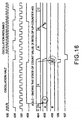
- an oscillation signal 105 is divided into the m number by a divider 402 in an oscillation monitoring circuit 50, the divided signal is given to the up-counter 403 of X-bits, and the up-counter 403 performs up-count.
- An output of the up-counter 403 is given to flip-flops 404, 405 of X-bits in X-bits state.
- the flip-flop 404 operates at a rising timing of a signal which is n-divided a referential signal 101 by the divider 407, and the flip-flop 405 operates at a falling timing. Thereby, a count value (X bits) of the up counter 403 is produced and retained.
- the output signals 456, 455 of the flip-flops 404, 405 are always put into different state. Under this circumstance, the monitor signal 106 produces the high level which indicates the oscillation state.
- the monitor signal 106 is equal to an output of an exclusive OR-gate 406 which is given with the output signal 456 of the flip-flop 404 and the output signal 455 of the flip-flop 405.
- the oscillation control signal 107 as the output of the oscillation control circuit 60 also becomes the high level, and the voltage control oscillator 30 is not particularly controlled.
- the outputs 456, 455 of the flip-flops 404, 405 become the same states (DH in Fig. 16). Further, the monitor signal 106 as the output of the exclusive OR-gate 406 produces the low level which indicates the oscillation halting state, and the oscillation control signal 107 as the output of the oscillation control circuit 60 becomes the low level when the referential signal 101 falls so as to reset the voltage control oscillator 30 into the oscillationable state.
- the oscillation control signal 107 puts the flip-flop 404 of the oscillation monitoring circuit 50 into the set state (high level output), puts the flip-flop 405 into the reset state (low level output), and puts the output of the exclusive OR-gate 406 into the high level. Thereby, the oscillation control signal 107 is put into the high level when the referential signal 101 subsequently falls.
Landscapes
- Stabilization Of Oscillater, Synchronisation, Frequency Synthesizers (AREA)
Applications Claiming Priority (2)
| Application Number | Priority Date | Filing Date | Title |
|---|---|---|---|
| JP23783498 | 1998-08-24 | ||
| JP10237834A JP2990171B1 (ja) | 1998-08-24 | 1998-08-24 | Pll回路とその制御方法 |
Publications (2)
| Publication Number | Publication Date |
|---|---|
| EP0987822A2 true EP0987822A2 (fr) | 2000-03-22 |
| EP0987822A3 EP0987822A3 (fr) | 2000-08-30 |
Family
ID=17021109
Family Applications (1)
| Application Number | Title | Priority Date | Filing Date |
|---|---|---|---|
| EP99116166A Withdrawn EP0987822A3 (fr) | 1998-08-24 | 1999-08-23 | Circuit PLL avec oscillateur en anneau et méthode de côntrole |
Country Status (5)
| Country | Link |
|---|---|
| US (1) | US6163224A (fr) |
| EP (1) | EP0987822A3 (fr) |
| JP (1) | JP2990171B1 (fr) |
| KR (1) | KR100341105B1 (fr) |
| CN (1) | CN1248823A (fr) |
Cited By (11)
| Publication number | Priority date | Publication date | Assignee | Title |
|---|---|---|---|---|
| WO2001029966A1 (fr) * | 1999-10-21 | 2001-04-26 | Sun Microsystems, Inc. | Oscillateur annulaire |
| EP1179886A2 (fr) * | 2000-07-31 | 2002-02-13 | Seiko Epson Corporation | Oscillateur et méthode de son controle |
| EP1294093A1 (fr) * | 2001-09-18 | 2003-03-19 | Altera Corporation | Cellues à retard programmable pour oscillateur commandé en tension |
| US6924678B2 (en) | 2003-10-21 | 2005-08-02 | Altera Corporation | Programmable phase-locked loop circuitry for programmable logic device |
| US7019570B2 (en) | 2003-09-05 | 2006-03-28 | Altera Corporation | Dual-gain loop circuitry for programmable logic device |
| US7075365B1 (en) | 2004-04-22 | 2006-07-11 | Altera Corporation | Configurable clock network for programmable logic device |
| US7230495B2 (en) | 2004-04-28 | 2007-06-12 | Micron Technology, Inc. | Phase-locked loop circuits with reduced lock time |
| US7436228B1 (en) | 2005-12-22 | 2008-10-14 | Altera Corporation | Variable-bandwidth loop filter methods and apparatus |
| US7937608B2 (en) | 2006-12-28 | 2011-05-03 | Realtek Semiconductor Corp. | Clock generating circuit and digital circuit system incorporating the same |
| US8120429B1 (en) | 2006-05-19 | 2012-02-21 | Altera Corporation | Voltage-controlled oscillator methods and apparatus |
| DE102009059852B4 (de) * | 2008-12-22 | 2020-10-15 | Denso Corporation | Impulsverzögerungs-Vorrichtung mit gerader Stufenanzahl |
Families Citing this family (25)
| Publication number | Priority date | Publication date | Assignee | Title |
|---|---|---|---|---|
| JP2001209454A (ja) * | 2000-01-27 | 2001-08-03 | Sony Corp | クロック生成回路 |
| JP2001257567A (ja) * | 2000-03-08 | 2001-09-21 | Hitachi Ltd | 電圧制御発振器およびpll回路および半導体集積回路装置 |
| US6593820B2 (en) * | 2001-08-10 | 2003-07-15 | Agilent Technologies, Inc. | High frequency voltage controlled oscillator |
| US6885233B2 (en) | 2002-05-02 | 2005-04-26 | Intel Corporation | Altering operating frequency and voltage set point of a circuit in response to the operating temperature and instantaneous operating voltage of the circuit |
| US6809606B2 (en) * | 2002-05-02 | 2004-10-26 | Intel Corporation | Voltage ID based frequency control for clock generating circuit |
| US6885252B2 (en) * | 2002-07-09 | 2005-04-26 | Mediatex Inc. | Clock recovery circuit capable of automatically adjusting frequency range of a VCO |
| US7031372B2 (en) * | 2003-04-22 | 2006-04-18 | Motorola, Inc. | Multiple user reconfigurable CDMA processor |
| US7254208B2 (en) * | 2003-05-20 | 2007-08-07 | Motorola, Inc. | Delay line based multiple frequency generator circuits for CDMA processing |
| US7114069B2 (en) * | 2003-04-22 | 2006-09-26 | Motorola, Inc. | Reconfigurable processing circuit including a delay locked loop multiple frequency generator for generating a plurality of clock signals which are configured in frequency by a control processor |
| US7064620B1 (en) * | 2003-05-09 | 2006-06-20 | Altera Corporation | Sequential VCO phase output enabling circuit |
| JP4805547B2 (ja) * | 2004-03-19 | 2011-11-02 | ルネサスエレクトロニクス株式会社 | 位相同期回路のジッタ検出回路 |
| US7145373B2 (en) * | 2004-07-29 | 2006-12-05 | Intel Corporation | Frequency-controlled DLL bias |
| US20060267659A1 (en) * | 2005-05-26 | 2006-11-30 | Jiu-Liang Tsai | High-speed, low-noise voltage-controlled delay cell |
| KR100803360B1 (ko) * | 2006-09-14 | 2008-02-14 | 주식회사 하이닉스반도체 | Pll 회로 및 그 제어 방법 |
| US20080211590A1 (en) * | 2007-03-01 | 2008-09-04 | Stephen Wu | Method and system for a varactor-tuned voltage-controlled ring oscillator with frequency and amplitude calibration |
| US9054711B2 (en) * | 2009-07-02 | 2015-06-09 | Infineon Technologies Ag | Frequency divider |
| JP5663881B2 (ja) | 2010-01-18 | 2015-02-04 | 富士通株式会社 | クロック装置 |
| JP5302235B2 (ja) * | 2010-02-09 | 2013-10-02 | ルネサスエレクトロニクス株式会社 | 半導体集積回路装置 |
| JP2010273386A (ja) * | 2010-08-16 | 2010-12-02 | Renesas Electronics Corp | 電圧制御発振器 |
| CN104834581B (zh) * | 2015-05-11 | 2018-07-06 | 江苏宏云技术有限公司 | 一种晶体振荡器的停振监测电路 |
| CN108933594B (zh) * | 2017-05-22 | 2022-01-11 | 中芯国际集成电路制造(上海)有限公司 | 压控振荡器及锁相环 |
| US10958277B1 (en) | 2019-09-05 | 2021-03-23 | Cobham Colorado Springs Inc. | PLL with multiple and adjustable phase outputs |
| CN113452367A (zh) * | 2020-03-27 | 2021-09-28 | 奇景光电股份有限公司 | 振荡电路及自启动控制电路 |
| CN112234952B (zh) * | 2020-09-29 | 2022-09-06 | 上海兆芯集成电路有限公司 | 振荡器电路 |
| JP2022154908A (ja) * | 2021-03-30 | 2022-10-13 | ラピステクノロジー株式会社 | リングオシレータ、およびリングオシレータの起動方法 |
Citations (5)
| Publication number | Priority date | Publication date | Assignee | Title |
|---|---|---|---|---|
| US5355097A (en) * | 1992-09-11 | 1994-10-11 | Cypress Semiconductor Corporation | Potentiometric oscillator with reset and test input |
| JPH0774625A (ja) * | 1993-09-03 | 1995-03-17 | Fujitsu Ltd | Pll発振回路 |
| US5596302A (en) * | 1996-01-17 | 1997-01-21 | Lucent Technologies Inc. | Ring oscillator using even numbers of differential stages with current mirrors |
| US5767748A (en) * | 1996-02-08 | 1998-06-16 | Kabushiki Kaisha Toshiba | Voltage controlled oscillator and voltage controlled delay circuit |
| US5796313A (en) * | 1996-04-25 | 1998-08-18 | Waferscale Integration Inc. | Low power programmable ring oscillator |
Family Cites Families (11)
| Publication number | Priority date | Publication date | Assignee | Title |
|---|---|---|---|---|
| JPS59179B2 (ja) * | 1978-09-22 | 1984-01-05 | 株式会社日立製作所 | クロック監視方式 |
| JPS5859653A (ja) * | 1982-07-21 | 1983-04-08 | Nec Corp | 位相同期回路 |
| JPS63185121A (ja) * | 1987-01-27 | 1988-07-30 | Matsushita Electric Ind Co Ltd | 発振停止防止回路 |
| JPH0420016A (ja) * | 1990-05-14 | 1992-01-23 | Hitachi Ltd | クロックジェネレータ及び半導体集積回路 |
| JPH05122032A (ja) * | 1991-10-28 | 1993-05-18 | Okuma Mach Works Ltd | 発振停止検出装置 |
| JP2734380B2 (ja) * | 1994-09-06 | 1998-03-30 | 日本電気株式会社 | 電圧制御発振器およびフェーズロックドループ回路 |
| JPH08307460A (ja) * | 1995-05-10 | 1996-11-22 | Yamaha Corp | デジタル信号伝送路 |
| JP3708168B2 (ja) * | 1995-06-13 | 2005-10-19 | 富士通株式会社 | 遅延装置 |
| JP3508412B2 (ja) * | 1995-08-10 | 2004-03-22 | セイコーエプソン株式会社 | データ復号回路、電圧制御発振回路、データ復号装置及び電子機器 |
| JPH09326692A (ja) * | 1996-06-04 | 1997-12-16 | Texas Instr Japan Ltd | 位相同期ループ回路 |
| JPH1168559A (ja) * | 1997-08-20 | 1999-03-09 | Nec Corp | 位相同期ループ回路 |
-
1998
- 1998-08-24 JP JP10237834A patent/JP2990171B1/ja not_active Expired - Fee Related
-
1999
- 1999-08-23 EP EP99116166A patent/EP0987822A3/fr not_active Withdrawn
- 1999-08-23 US US09/378,707 patent/US6163224A/en not_active Expired - Fee Related
- 1999-08-23 KR KR1019990035033A patent/KR100341105B1/ko not_active IP Right Cessation
- 1999-08-24 CN CN99111699A patent/CN1248823A/zh active Pending
Patent Citations (5)
| Publication number | Priority date | Publication date | Assignee | Title |
|---|---|---|---|---|
| US5355097A (en) * | 1992-09-11 | 1994-10-11 | Cypress Semiconductor Corporation | Potentiometric oscillator with reset and test input |
| JPH0774625A (ja) * | 1993-09-03 | 1995-03-17 | Fujitsu Ltd | Pll発振回路 |
| US5596302A (en) * | 1996-01-17 | 1997-01-21 | Lucent Technologies Inc. | Ring oscillator using even numbers of differential stages with current mirrors |
| US5767748A (en) * | 1996-02-08 | 1998-06-16 | Kabushiki Kaisha Toshiba | Voltage controlled oscillator and voltage controlled delay circuit |
| US5796313A (en) * | 1996-04-25 | 1998-08-18 | Waferscale Integration Inc. | Low power programmable ring oscillator |
Non-Patent Citations (1)
| Title |
|---|
| PATENT ABSTRACTS OF JAPAN vol. 1995, no. 06, 31 July 1995 (1995-07-31) & JP 07 074625 A (FUJITSU LTD), 17 March 1995 (1995-03-17) * |
Cited By (19)
| Publication number | Priority date | Publication date | Assignee | Title |
|---|---|---|---|---|
| WO2001029966A1 (fr) * | 1999-10-21 | 2001-04-26 | Sun Microsystems, Inc. | Oscillateur annulaire |
| GB2372652A (en) * | 1999-10-21 | 2002-08-28 | Sun Microsystems Inc | Ring oscillator |
| EP1179886A2 (fr) * | 2000-07-31 | 2002-02-13 | Seiko Epson Corporation | Oscillateur et méthode de son controle |
| EP1179886A3 (fr) * | 2000-07-31 | 2003-01-02 | Seiko Epson Corporation | Oscillateur et méthode de son controle |
| US6670860B2 (en) | 2000-07-31 | 2003-12-30 | Seiko Epson Corporation | Oscillator and control method for controlling the oscillator |
| EP1294093A1 (fr) * | 2001-09-18 | 2003-03-19 | Altera Corporation | Cellues à retard programmable pour oscillateur commandé en tension |
| US6771105B2 (en) | 2001-09-18 | 2004-08-03 | Altera Corporation | Voltage controlled oscillator programmable delay cells |
| US7151397B2 (en) | 2001-09-18 | 2006-12-19 | Altera Corporation | Voltage controlled oscillator programmable delay cells |
| US7019570B2 (en) | 2003-09-05 | 2006-03-28 | Altera Corporation | Dual-gain loop circuitry for programmable logic device |
| US7071743B2 (en) | 2003-10-21 | 2006-07-04 | Altera Corporation | Programmable phase-locked loop circuitry for programmable logic device |
| US6924678B2 (en) | 2003-10-21 | 2005-08-02 | Altera Corporation | Programmable phase-locked loop circuitry for programmable logic device |
| US7307459B2 (en) | 2003-10-21 | 2007-12-11 | Altera Corporation | Programmable phase-locked loop circuitry for programmable logic device |
| US7075365B1 (en) | 2004-04-22 | 2006-07-11 | Altera Corporation | Configurable clock network for programmable logic device |
| US7286007B1 (en) | 2004-04-22 | 2007-10-23 | Altera Corporation | Configurable clock network for programmable logic device |
| US7230495B2 (en) | 2004-04-28 | 2007-06-12 | Micron Technology, Inc. | Phase-locked loop circuits with reduced lock time |
| US7436228B1 (en) | 2005-12-22 | 2008-10-14 | Altera Corporation | Variable-bandwidth loop filter methods and apparatus |
| US8120429B1 (en) | 2006-05-19 | 2012-02-21 | Altera Corporation | Voltage-controlled oscillator methods and apparatus |
| US7937608B2 (en) | 2006-12-28 | 2011-05-03 | Realtek Semiconductor Corp. | Clock generating circuit and digital circuit system incorporating the same |
| DE102009059852B4 (de) * | 2008-12-22 | 2020-10-15 | Denso Corporation | Impulsverzögerungs-Vorrichtung mit gerader Stufenanzahl |
Also Published As
| Publication number | Publication date |
|---|---|
| CN1248823A (zh) | 2000-03-29 |
| JP2000068825A (ja) | 2000-03-03 |
| US6163224A (en) | 2000-12-19 |
| KR100341105B1 (ko) | 2002-06-20 |
| EP0987822A3 (fr) | 2000-08-30 |
| JP2990171B1 (ja) | 1999-12-13 |
| KR20000017468A (ko) | 2000-03-25 |
Similar Documents
| Publication | Publication Date | Title |
|---|---|---|
| US6163224A (en) | PLL circuit and method of controlling the same | |
| US8260835B2 (en) | Random number generator with ring oscillation circuit | |
| US4905176A (en) | Random number generator circuit | |
| US5425074A (en) | Fast programmable/resettable CMOS Johnson counters | |
| US5399995A (en) | CMOS circuit providing 90 degree phase delay | |
| JP4559985B2 (ja) | 乱数発生回路 | |
| US5448193A (en) | Normalization of apparent propagation delay | |
| US5426384A (en) | Voltage controlled oscillator (VCO) with symmetrical output and logic gate for use in same | |
| US5619170A (en) | PLL timing generator with voltage controlled oscillator | |
| US6914460B1 (en) | Counter-based clock doubler circuits and methods | |
| TWI442704B (zh) | 用以在一特定時間間隔過程中計數輸入脈衝之裝置 | |
| US6750692B2 (en) | Circuit and method for generating internal clock signal | |
| US20040008063A1 (en) | Delay locked loop clock generator | |
| US8063686B1 (en) | Phase interpolator circuit with two phase capacitor charging | |
| JPH07264059A (ja) | 位相差又は周波数差の検出回路 | |
| KR20060047261A (ko) | 교차 결합된 전압 제어 발진기 | |
| US5898242A (en) | Self-calibrating clock circuit employing a continuously variable delay module in a feedback loop | |
| US6525588B2 (en) | Clock control circuit and method | |
| US5434806A (en) | Apparatus and method for random number generation | |
| EP0238874B1 (fr) | Générateur de signaux temporels à résolution double de la fréquence d'horloge | |
| EP0651505A1 (fr) | Oscillateur en anneau CMOS commandé en tension | |
| KR20070071141A (ko) | 지연 고정 루프 기반의 주파수 체배 기능을 갖는 클럭발생기 | |
| US6177812B1 (en) | Phase detector | |
| US6661864B2 (en) | Counter circuit for detecting erroneous operation and recovering to normal operation by itself | |
| KR20190046421A (ko) | 듀티 싸이클 감지기 및 위상 차이 감지기 |
Legal Events
| Date | Code | Title | Description |
|---|---|---|---|
| PUAI | Public reference made under article 153(3) epc to a published international application that has entered the european phase |
Free format text: ORIGINAL CODE: 0009012 |
|
| AK | Designated contracting states |
Kind code of ref document: A2 Designated state(s): DE FR GB IT NL |
|
| AX | Request for extension of the european patent |
Free format text: AL;LT;LV;MK;RO;SI |
|
| PUAL | Search report despatched |
Free format text: ORIGINAL CODE: 0009013 |
|
| AK | Designated contracting states |
Kind code of ref document: A3 Designated state(s): AT BE CH CY DE DK ES FI FR GB GR IE IT LI LU MC NL PT SE |
|
| AX | Request for extension of the european patent |
Free format text: AL;LT;LV;MK;RO;SI |
|
| 17P | Request for examination filed |
Effective date: 20000721 |
|
| AKX | Designation fees paid |
Free format text: DE FR GB IT NL |
|
| 17Q | First examination report despatched |
Effective date: 20020201 |
|
| RAP1 | Party data changed (applicant data changed or rights of an application transferred) |
Owner name: NEC ELECTRONICS CORPORATION |
|
| GRAH | Despatch of communication of intention to grant a patent |
Free format text: ORIGINAL CODE: EPIDOS IGRA |
|
| STAA | Information on the status of an ep patent application or granted ep patent |
Free format text: STATUS: THE APPLICATION IS DEEMED TO BE WITHDRAWN |
|
| 18D | Application deemed to be withdrawn |
Effective date: 20031016 |