EP0982776A2 - Thyristor de protection ESD avec diode de déclenchement - Google Patents
Thyristor de protection ESD avec diode de déclenchement Download PDFInfo
- Publication number
- EP0982776A2 EP0982776A2 EP99306769A EP99306769A EP0982776A2 EP 0982776 A2 EP0982776 A2 EP 0982776A2 EP 99306769 A EP99306769 A EP 99306769A EP 99306769 A EP99306769 A EP 99306769A EP 0982776 A2 EP0982776 A2 EP 0982776A2
- Authority
- EP
- European Patent Office
- Prior art keywords
- type
- electrostatic discharge
- discharge protection
- impurity concentration
- concentration region
- Prior art date
- Legal status (The legal status is an assumption and is not a legal conclusion. Google has not performed a legal analysis and makes no representation as to the accuracy of the status listed.)
- Granted
Links
- 239000012535 impurity Substances 0.000 claims abstract description 281
- 239000004065 semiconductor Substances 0.000 claims abstract description 194
- 239000012212 insulator Substances 0.000 claims abstract description 56
- 229910021332 silicide Inorganic materials 0.000 claims abstract description 40
- FVBUAEGBCNSCDD-UHFFFAOYSA-N silicide(4-) Chemical compound [Si-4] FVBUAEGBCNSCDD-UHFFFAOYSA-N 0.000 claims abstract description 40
- 239000000758 substrate Substances 0.000 claims description 104
- 238000000034 method Methods 0.000 claims description 42
- 229910021420 polycrystalline silicon Inorganic materials 0.000 claims description 34
- 229920005591 polysilicon Polymers 0.000 claims description 34
- 238000004519 manufacturing process Methods 0.000 claims description 32
- 238000000926 separation method Methods 0.000 claims description 29
- 238000002513 implantation Methods 0.000 claims description 27
- 238000005468 ion implantation Methods 0.000 claims description 17
- 150000002500 ions Chemical class 0.000 claims description 16
- XUIMIQQOPSSXEZ-UHFFFAOYSA-N Silicon Chemical compound [Si] XUIMIQQOPSSXEZ-UHFFFAOYSA-N 0.000 claims description 11
- 229910052710 silicon Inorganic materials 0.000 claims description 11
- 239000010703 silicon Substances 0.000 claims description 11
- 238000000059 patterning Methods 0.000 claims description 4
- 239000010410 layer Substances 0.000 description 29
- 230000015556 catabolic process Effects 0.000 description 28
- 229920002120 photoresistant polymer Polymers 0.000 description 26
- 238000010586 diagram Methods 0.000 description 15
- 229910052751 metal Inorganic materials 0.000 description 13
- 239000002184 metal Substances 0.000 description 13
- 230000000694 effects Effects 0.000 description 8
- 238000002844 melting Methods 0.000 description 8
- 230000008018 melting Effects 0.000 description 8
- 230000002441 reversible effect Effects 0.000 description 6
- 230000001960 triggered effect Effects 0.000 description 5
- 230000015572 biosynthetic process Effects 0.000 description 4
- GZPBVLUEICLBOA-UHFFFAOYSA-N 4-(dimethylamino)-3,5-dimethylphenol Chemical compound CN(C)C1=C(C)C=C(O)C=C1C GZPBVLUEICLBOA-UHFFFAOYSA-N 0.000 description 3
- 238000010438 heat treatment Methods 0.000 description 3
- 238000007254 oxidation reaction Methods 0.000 description 3
- 238000000151 deposition Methods 0.000 description 2
- 230000008030 elimination Effects 0.000 description 2
- 238000003379 elimination reaction Methods 0.000 description 2
- 238000005530 etching Methods 0.000 description 2
- 238000002347 injection Methods 0.000 description 2
- 239000007924 injection Substances 0.000 description 2
- 239000011229 interlayer Substances 0.000 description 2
- 230000000670 limiting effect Effects 0.000 description 2
- 238000000206 photolithography Methods 0.000 description 2
- 230000002829 reductive effect Effects 0.000 description 2
- ZOXJGFHDIHLPTG-UHFFFAOYSA-N Boron Chemical compound [B] ZOXJGFHDIHLPTG-UHFFFAOYSA-N 0.000 description 1
- RTAQQCXQSZGOHL-UHFFFAOYSA-N Titanium Chemical compound [Ti] RTAQQCXQSZGOHL-UHFFFAOYSA-N 0.000 description 1
- 229910045601 alloy Inorganic materials 0.000 description 1
- 239000000956 alloy Substances 0.000 description 1
- 229910052796 boron Inorganic materials 0.000 description 1
- 229910017052 cobalt Inorganic materials 0.000 description 1
- 239000010941 cobalt Substances 0.000 description 1
- GUTLYIVDDKVIGB-UHFFFAOYSA-N cobalt atom Chemical compound [Co] GUTLYIVDDKVIGB-UHFFFAOYSA-N 0.000 description 1
- 239000004020 conductor Substances 0.000 description 1
- 230000005611 electricity Effects 0.000 description 1
- 230000002401 inhibitory effect Effects 0.000 description 1
- 238000009413 insulation Methods 0.000 description 1
- 238000002955 isolation Methods 0.000 description 1
- 238000012986 modification Methods 0.000 description 1
- 230000004048 modification Effects 0.000 description 1
- 230000003647 oxidation Effects 0.000 description 1
- 230000003068 static effect Effects 0.000 description 1
- 239000010936 titanium Substances 0.000 description 1
- 229910052719 titanium Inorganic materials 0.000 description 1
- 230000001052 transient effect Effects 0.000 description 1
Images


Classifications
-
- H—ELECTRICITY
- H01—ELECTRIC ELEMENTS
- H01L—SEMICONDUCTOR DEVICES NOT COVERED BY CLASS H10
- H01L27/00—Devices consisting of a plurality of semiconductor or other solid-state components formed in or on a common substrate
- H01L27/02—Devices consisting of a plurality of semiconductor or other solid-state components formed in or on a common substrate including semiconductor components specially adapted for rectifying, oscillating, amplifying or switching and having potential barriers; including integrated passive circuit elements having potential barriers
- H01L27/04—Devices consisting of a plurality of semiconductor or other solid-state components formed in or on a common substrate including semiconductor components specially adapted for rectifying, oscillating, amplifying or switching and having potential barriers; including integrated passive circuit elements having potential barriers the substrate being a semiconductor body
-
- H—ELECTRICITY
- H01—ELECTRIC ELEMENTS
- H01L—SEMICONDUCTOR DEVICES NOT COVERED BY CLASS H10
- H01L27/00—Devices consisting of a plurality of semiconductor or other solid-state components formed in or on a common substrate
- H01L27/02—Devices consisting of a plurality of semiconductor or other solid-state components formed in or on a common substrate including semiconductor components specially adapted for rectifying, oscillating, amplifying or switching and having potential barriers; including integrated passive circuit elements having potential barriers
- H01L27/0203—Particular design considerations for integrated circuits
- H01L27/0248—Particular design considerations for integrated circuits for electrical or thermal protection, e.g. electrostatic discharge [ESD] protection
- H01L27/0251—Particular design considerations for integrated circuits for electrical or thermal protection, e.g. electrostatic discharge [ESD] protection for MOS devices
- H01L27/0259—Particular design considerations for integrated circuits for electrical or thermal protection, e.g. electrostatic discharge [ESD] protection for MOS devices using bipolar transistors as protective elements
- H01L27/0262—Particular design considerations for integrated circuits for electrical or thermal protection, e.g. electrostatic discharge [ESD] protection for MOS devices using bipolar transistors as protective elements including a PNP transistor and a NPN transistor, wherein each of said transistors has its base coupled to the collector of the other transistor, e.g. silicon controlled rectifier [SCR] devices
-
- H—ELECTRICITY
- H01—ELECTRIC ELEMENTS
- H01L—SEMICONDUCTOR DEVICES NOT COVERED BY CLASS H10
- H01L27/00—Devices consisting of a plurality of semiconductor or other solid-state components formed in or on a common substrate
- H01L27/02—Devices consisting of a plurality of semiconductor or other solid-state components formed in or on a common substrate including semiconductor components specially adapted for rectifying, oscillating, amplifying or switching and having potential barriers; including integrated passive circuit elements having potential barriers
- H01L27/0203—Particular design considerations for integrated circuits
- H01L27/0248—Particular design considerations for integrated circuits for electrical or thermal protection, e.g. electrostatic discharge [ESD] protection
- H01L27/0251—Particular design considerations for integrated circuits for electrical or thermal protection, e.g. electrostatic discharge [ESD] protection for MOS devices
- H01L27/0259—Particular design considerations for integrated circuits for electrical or thermal protection, e.g. electrostatic discharge [ESD] protection for MOS devices using bipolar transistors as protective elements
-
- H—ELECTRICITY
- H01—ELECTRIC ELEMENTS
- H01L—SEMICONDUCTOR DEVICES NOT COVERED BY CLASS H10
- H01L29/00—Semiconductor devices specially adapted for rectifying, amplifying, oscillating or switching and having potential barriers; Capacitors or resistors having potential barriers, e.g. a PN-junction depletion layer or carrier concentration layer; Details of semiconductor bodies or of electrodes thereof ; Multistep manufacturing processes therefor
- H01L29/66—Types of semiconductor device ; Multistep manufacturing processes therefor
- H01L29/68—Types of semiconductor device ; Multistep manufacturing processes therefor controllable by only the electric current supplied, or only the electric potential applied, to an electrode which does not carry the current to be rectified, amplified or switched
- H01L29/70—Bipolar devices
- H01L29/74—Thyristor-type devices, e.g. having four-zone regenerative action
- H01L29/7404—Thyristor-type devices, e.g. having four-zone regenerative action structurally associated with at least one other device
- H01L29/7412—Thyristor-type devices, e.g. having four-zone regenerative action structurally associated with at least one other device the device being a diode
Definitions
- the present invention relates to an electrostatic discharge protection device used in a semiconductor integrated circuit for protecting the semiconductor integrated circuit from breaking due to an electrostatic charge flowing into or out of the circuit (electrostatic discharge phenomenon).
- the present invention also relates to a method for producing such an electrostatic discharge protection device, and an electrostatic discharge protection circuit using the same.
- the electrostatic discharge is a phenomenon in which an electrostatic charge flows into a semiconductor integrated circuit from an electrostatically charged person or machine, or an electrostatic charge flows into an external conductor from a semiconductor integrated circuit which has been electrostatically charged by friction, etc.
- an amount of electrostatic charge flows into or out of a semiconductor integrated circuit in a moment.
- an excessive current flows through the semiconductor integrated circuit device, whereby an excessive voltage flows through an internal circuit. Consequently, junction breakdown, line melting, oxide film dielectric breakdown, or the like, may occur, thereby breaking the semiconductor integrated circuit.
- an electrostatic discharge protection device is commonly provided between an external terminal and an internal circuit of a semiconductor integrated circuit so as to form a bypass circuit for static electricity.
- Such an electrostatic discharge protection device is provided during a step in the production of the semiconductor integrated circuit.
- Commonly-employed electrostatic discharge protection devices include current limiting elements for limiting a transient current flowing in a semiconductor integrated circuit, such as a diffused resistor, and a polysilicon resistor.
- Other such protection circuits include a voltage clamping element for suppressing the voltage applied to an internal circuit, such as a diode, a thyristor, a MOS transistor, and a bipolar transistor.
- a thyristor as a current clamping element, can advantageously produce an excessive discharge current.
- a trigger voltage at which the thyristor is turned ON is generally high, e.g., about 25 V to about 40 V, whereby the semiconductor integrated circuit may break before the thyristor is activated.
- thyristors have been adjusted to reduce the trigger voltage.
- Figure 24 is a cross-sectional view illustrating an exemplary conventional electrostatic discharge protection device, and more particularly, a thyristor that can be triggered by a low voltage (Japanese Patent No. 2505652).
- an n-type well 2 is provided in a p-type substrate 1 as an n-type impurity diffused layer.
- a p-type anode high impurity concentration region 4 and an n-type anode gate high impurity concentration region 5 are provided in the n-type well 2 .
- a p-type high impurity concentration region 55 is provided across the boundary between the n-type well 2 and the p-type substrate 1 , so that a portion of the p-type high impurity concentration region 55 is surrounded by the n-type well 2 and another portion thereof is surrounded by the p-type substrate 1 .
- An n-type cathode high impurity concentration region 6 and a p-type cathode gate high impurity concentration region 7 are provided in another region of the p-type substrate 1 away from the n-type well 2 .
- the p-type anode high impurity concentration region 4 and the n-type anode gate high impurity concentration region 5 are connected to an anode terminal 36 via a contact 16 and a metal 18.
- the n-type cathode high impurity concentration region 6 and the p-type cathode gate high impurity concentration region 7 are connected to a cathode terminal 54 via another contact 16 and another metal 53 .
- the low voltage thyristor as illustrated in Figure 24 may be provided between a power supply line 52 and a reference voltage line 45 of a semiconductor integrated circuit.
- An anode terminal 36 of the electrostatic discharge protection device 56 is connected to the power supply line 52, and the cathode terminal 54 of the electrostatic discharge protection device 56 is connected to the reference voltage line 45.
- An excessive voltage due to an electrostatic discharge is applied to the power supply line 52 .
- the electrostatic discharge reaches the trigger voltage of the thyristor provided in the electrostatic discharge protection device 56
- the thyristor is turned ON, thereby forming a low-resistance path between the power supply line 52 and the reference voltage line 45 .
- the low-resistance path bypasses an electrostatic charge flowing into the device from a power supply terminal 51 to a reference voltage terminal 44 , thereby preventing breakdown of a semiconductor integrated circuit 57 connected to the power supply line 52 and the reference voltage line 45 .
- the trigger voltage of the thyristor is determined by the breakdown voltage between the p-type substrate 1 and the n-type well 2 .
- the trigger voltage will be as high as about 25 V to about 40 V. With such a high voltage, internal circuits of the semiconductor integrated circuit 57 will break before the thyristor is turned ON.
- the trigger voltage of the thyristor illustrated in Figure 24 is determined by the breakdown voltage between the p-type high impurity concentration region 55 and the n-type well 2 . Due to the presence of the p-type high impurity concentration region 55 , the breakdown voltage can be reduced below the breakdown voltage between the p-type substrate 1 and the n-type well 2 .
- a salicide (self-alignment silicide) step has been employed in order to reduce the source/drain diffused resistance or the gate line resistance of a MOS transistor.
- a silicon substrate surface and a polysilicon surface whose resistances are to be reduced, are first adjusted to be exposed, on which a high melting point metal such as titanium or cobalt is deposited. Then, a heat treatment is performed so as to provide an alloy (silicide) of silicon and the high melting point metal.
- a silicide layer is provided on a portion of a silicon surface which is not covered with a gate oxide film or a device separation insulator of the MOS transistor.
- the silicon surfaces of the p-type high impurity concentration region 55 (to be the trigger) and the n-type well 2 are both covered with the silicide layer. Then, the p-type high impurity concentration region 55 and the n-type well 2 are shortcircuitted with each other, whereby breakdown can no longer occur therebetween.
- the n-type anode gate high impurity concentration region 5 , the n-type well 2 , the p-type high impurity concentration region 55 , the p-type substrate 1 , and the p-type cathode gate high impurity concentration region 7 are shortcircuitted with one another, whereby the anode terminal 36 and the cathode terminal 54 are shortcircuitted with each other.
- a way of avoiding the shortcircuit between the p-type high impurity concentration region 55 and the n-type well 2 is to provide a silicidation inhibiting insulator on the silicon surface of the pn junction between the p-type high impurity concentration region 55 and the n-type well 2 , in a step separate from the step of forming a semiconductor integrated circuit and prior to the salicide step.
- This method adds a further step or photomask to the semiconductor integrated circuit process, thereby increasing the production cost of the semiconductor integrated circuit.
- an electrostatic discharge protection device is provided at an input or an output of a semiconductor integrated circuit for protecting an internal circuit of the semiconductor integrated circuit from an electrostatic surge flowing into or out of the semiconductor integrated circuit.
- the electrostatic discharge protection device includes: a thyristor; and a trigger diode for triggering the thyristor with a low voltage.
- the trigger diode includes: an n-type cathode high impurity concentration region; a p-type anode high impurity concentration region; and an insulator section for electrically insulating a silicide layer formed on a surface of the n-type cathode high impurity concentration region from another silicide layer formed on a surface of the p-type anode high impurity concentration region.
- the insulator section includes: a gate oxide film formed between the n-type cathode high impurity concentration region and the p-type anode high impurity concentration region for providing a gate of a MOS transistor of the semiconductor integrated circuit; a polysilicon patterned on the gate oxide film; and a gate sidewall insulator provided on a sidewall of the gate oxide film and a sidewall of the polysilicon for electrically insulating the silicide layer formed on the surface of the n-type cathode high impurity concentration region from the silicide layer formed on the surface of the p-type anode high impurity concentration region.
- the electrostatic discharge protection device is formed in a p-type semiconductor substrate.
- the n-type cathode high impurity concentration region is formed in an n-type well.
- a portion of the p-type anode high impurity concentration region is included in the n-type well.
- Another portion of the p-type anode high impurity concentration region is included in the p-type semiconductor substrate or a p-type well.
- the electrostatic discharge protection device is formed in a p-type semiconductor substrate.
- the p-type anode high impurity concentration region is formed in the p-type semiconductor substrate or a p-type well.
- a portion of the n-type cathode high impurity concentration region is included in an n-type well.
- Another portion of the n-type cathode high impurity concentration region is included in the p-type semiconductor substrate or the p-type well.
- the electrostatic discharge protection device is formed in an n-type semiconductor substrate.
- the n-type cathode high impurity concentration region is formed in the n-type semiconductor substrate.
- a portion of the p-type anode high impurity concentration region is included in a p-type well.
- Another portion of the p-type anode high impurity concentration region is included in the n-type semiconductor substrate or an n-type well.
- the electrostatic discharge protection device is formed in an n-type semiconductor substrate.
- the p-type anode high impurity concentration region is formed in a p-type well.
- a portion of the n-type cathode high impurity concentration region is included in the p-type well.
- Another portion of the n-type cathode high impurity concentration region is included in the n-type semiconductor substrate or an n-type well.
- the insulator section includes a device separation insulator which is formed between the n-type cathode high impurity concentration region and the p-type anode high impurity concentration region for providing a device separation region of a MOS transistor of the semiconductor integrated circuit.
- the electrostatic discharge protection device is formed in a p-type semiconductor substrate.
- the n-type cathode high impurity concentration region is formed in an n-type well.
- a portion of the p-type anode high impurity concentration region is included in the n-type well.
- Another portion of the p-type anode high impurity concentration region is included in the p-type semiconductor substrate or a p-type well.
- the electrostatic discharge protection device is formed in a p-type semiconductor substrate.
- the p-type anode high impurity concentration region is formed in the p-type semiconductor substrate or a p-type well.
- a portion of the n-type cathode high impurity concentration region is included in an n-type well.
- Another portion of the n-type cathode high impurity concentration region is included in the p-type semiconductor substrate or the p-type well.
- the electrostatic discharge protection device is formed in an n-type semiconductor substrate.
- the n-type cathode high impurity concentration region is formed in the n-type semiconductor substrate.
- a portion of the p-type anode high impurity concentration region is included in a p-type well.
- Another portion of the p-type anode high impurity concentration region is included in the n-type semiconductor substrate or an n-type well.
- the electrostatic discharge protection device is formed in an n-type semiconductor substrate.
- the p-type anode high impurity concentration region is formed in a p-type well.
- a portion of the n-type cathode high impurity concentration region is included in the p-type well.
- Another portion of the n-type cathode high impurity concentration region is included in the n-type semiconductor substrate or an n-type well.
- a method for producing an electrostatic discharge protection device of the present invention includes the steps of: forming an n-type cathode high impurity concentration region; forming a p-type anode high impurity concentration region; and forming an insulator section for electrically insulating a silicide layer formed on a surface of the n-type cathode high impurity concentration region from another silicide layer formed on a surface of the p-type anode high impurity concentration region.
- the step of forming the insulator section includes the steps of: forming, on a silicon substrate, a gate oxide film to be a gate of a MOS transistor of a semiconductor integrated circuit; patterning, on the gate oxide film, a polysilicon to be a gate electrode of the MOS transistor; implanting ions of a p-type impurity using the polysilicon and a p-type ion implantation resist as masks; implanting ions of an n-type impurity using the polysilicon and an n-type ion implantation resist as masks; forming a gate sidewall insulator on a sidewall of the polysilicon and a sidewall of the gate oxide film; and forming a silicide layer on a surface of the n-type cathode high impurity concentration region and a surface of the p-type anode high impurity concentration region.
- the method further includes, before the step of implanting ions of a p-type or n-type impurity, the step of: where the n-type cathode high impurity concentration region of the trigger diode of the thyristor forms a PN junction with a p-type substrate or a p-type well, arranging an edge of a p-type ion implantation photomask at a position in the polysilicon region which is shifted away from an edge of an n-type impurity implantation region.
- the method further includes, before the step of implanting ions of a p-type or n-type impurity, the step of: where the p-type cathode high impurity concentration region of the trigger diode of the thyristor forms a PN junction with an n-type substrate or an n-type well, arranging an edge of an n-type ion implantation photomask at a position in the polysilicon region which is shifted away from an edge of a p-type impurity implantation region.
- the step of forming the insulator section includes the steps of: forming a device separation insulator for separating an active region, in which a MOS transistor of the semiconductor integrated circuit is formed, from another such active region; implanting ions of a p-type impurity using the device separation insulator and a p-type ion implantation resist as masks; implanting ions of an n-type impurity using the device separation insulator and an n-type ion implantation resist as masks; and forming a silicide layer on a surface of the p-type anode high impurity concentration region and a surface of the n-type cathode high impurity concentration region.
- the method further includes, before the step of implanting ions of a p-type or n-type impurity, the step of: where the n-type cathode high impurity concentration region of the trigger diode of the thyristor forms a PN junction with a p-type substrate or a p-type well, arranging an edge of a p-type ion implantation photomask at a position on the device separation insulator at or near the center of the trigger diode which is shifted away from an edge of an n-type impurity implantation region.
- the method further includes, before the step of implanting ions of a p-type or n-type impurity, the step of: where the p-type anode high impurity concentration region of the trigger diode of the thyristor forms a PN junction with an n-type substrate or an n-type well, arranging an edge of an n-type ion implantation photomask at a position on the device separation insulator at or near the center of the trigger diode which is shifted away from an edge of a p-type impurity implantation region.
- an electrostatic discharge protection circuit for bypassing an electrostatic surge entering a semiconductor integrated circuit through an input/output terminal thereof to a reference voltage line.
- the electrostatic discharge protection circuit includes: the electrostatic discharge protection device having the trigger diode according to the present invention; and a protection diode.
- the electrostatic discharge protection device and the protection diode are arranged in parallel between an input/output signal line and the reference voltage line of the semiconductor integrated circuit.
- An anode and an anode gate of a thyristor provided in the electrostatic discharge protection device and a cathode of the protection diode are connected to the input/output signal line.
- a cathode and a cathode gate of the thyristor and an anode of the protection diode are connected to the reference voltage line.
- the electrostatic discharge protection device further includes a resistor, the resistor being formed in a well, which has a conductivity type opposite to that of a substrate, between the anode of the thyristor and the cathode of the protection diode.
- an electrostatic discharge protection circuit for bypassing an electrostatic surge entering a semiconductor integrated circuit through an input/output terminal thereof to a power supply line.
- the electrostatic discharge protection circuit includes: the electrostatic discharge protection device having the trigger diode according to the present invention; and a protection diode formed in an n-type substrate or an n-type well.
- the electrostatic discharge protection device and the protection diode are arranged in parallel between an input/output signal line and a power supply line of the semiconductor integrated circuit.
- An anode and an anode gate of a thyristor provided in the electrostatic discharge protection device and a cathode of the protection diode are connected to the power supply line of the semiconductor integrated circuit.
- a cathode of the thyristor and an anode of the protection diode are connected to the input/output signal line.
- a cathode gate of the thyristor is connected to the reference voltage line.
- the electrostatic discharge protection device further includes a resistor, the resistor being formed in a well, which has a conductivity type opposite to that of a substrate, between the cathode of the thyristor and the anode of the protection diode.
- an electrostatic discharge protection circuit for bypassing an electrostatic surge entering a semiconductor integrated circuit through a power supply line thereof to a reference voltage line.
- the electrostatic discharge protection circuit includes: the electrostatic discharge protection device having the trigger diode according to the present invention.
- the electrostatic discharge protection device is arranged between the power supply line and the reference voltage line of the semiconductor integrated circuit.
- An anode and an anode gate of a thyristor provided in the electrostatic discharge protection device are connected to the power supply line.
- a cathode and a cathode gate of the thyristor are connected to the reference voltage line.
- the n-type cathode high impurity concentration region and the p-type anode high impurity concentration region of the protection diode are produced according to the method of producing an electrostatic discharge protection device of the present invention.
- an electrostatic discharge protection circuit for bypassing an electrostatic surge entering a semiconductor integrated circuit through any of an input/output terminal, a reference voltage terminal, and a power supply line thereof, to another of the input/output terminal, the reference voltage terminal, and the power supply terminal.
- the electrostatic discharge protection circuit includes: a first electrostatic discharge protection circuit according to the present invention; a second electrostatic discharge protection circuit according to the present invention; and a third electrostatic discharge protection circuit according to the present invention.
- the first electrostatic discharge protection circuit is provided between an input/output signal line and a reference voltage line of the semiconductor integrated circuit.
- the second electrostatic discharge protection circuit is provided between the input/output signal line and a power supply line of the semiconductor integrated circuit.
- the third electrostatic discharge protection circuit is provided between the power supply line and the reference voltage line.
- an electrostatic discharge protection circuit for bypassing an electrostatic surge entering a semiconductor integrated circuit through any of an input/output terminal, a reference voltage terminal, and a power supply line thereof, to another of the input/output terminal, the reference voltage terminal, and the power supply terminal.
- the electrostatic discharge protection circuit includes first, second and third electrostatic discharge protection devices each having a trigger diode according to the present invention.
- An anode and an anode gate of a first thyristor provided in the first electrostatic discharge protection device are connected to a power supply line of the semiconductor integrated circuit.
- a cathode of the first thyristor is connected to an input/output signal line of the semiconductor integrated circuit.
- a cathode gate of the first thyristor is connected to a reference voltage line of the semiconductor integrated circuit.
- An anode and an anode gate of a second thyristor provided in the second electrostatic discharge protection device are connected to the input/output signal line of the semiconductor integrated circuit.
- a cathode and a cathode gate of the second thyristor are connected to the reference voltage line of the semiconductor integrated circuit.
- An anode and an anode gate of a third thyristor provided in the third electrostatic discharge protection device are connected to the power supply line of the semiconductor integrated circuit.
- a cathode and a cathode gate of the third thyristor are connected to the reference voltage line of the semiconductor integrated circuit.
- an electrostatic discharge protection circuit for bypassing an electrostatic surge entering a semiconductor integrated circuit through any of an input/output terminal, a reference voltage terminal, and a power supply line thereof, to another of the input/output terminal, the reference voltage terminal, and the power supply terminal.
- the electrostatic discharge protection circuit includes: a first electrostatic discharge protection circuit according to the present invention; and a second electrostatic discharge protection circuit according to the present invention.
- the first electrostatic discharge protection circuit is provided between an input/output signal line and a reference voltage line of the semiconductor integrated circuit.
- the second electrostatic discharge protection circuit is provided between a power supply line and the reference voltage line of the semiconductor integrated circuit.
- an electrostatic discharge protection circuit for bypassing an electrostatic surge entering a semiconductor integrated circuit through any of an input/output terminal, a reference voltage terminal, and a power supply line thereof, to another of the input/output terminal, the reference voltage terminal, and the power supply terminal, is provided.
- the electrostatic discharge protection circuit includes: a first electrostatic discharge protection device having a trigger diode according to the present invention between a reference voltage line and an input/output signal line of the semiconductor integrated circuit; and a second electrostatic discharge protection device having a trigger diode according to the present invention between the reference voltage line and a power supply line of the semiconductor integrated circuit.
- An anode and an anode gate of a first thyristor provided in the first electrostatic discharge protection device are connected to an input/output signal line of the semiconductor integrated circuit.
- a cathode and a cathode gate of the first thyristor are connected to the reference voltage line of the semiconductor integrated circuit.
- An anode and an anode gate of a second thyristor provided in the second electrostatic discharge protection device are connected to the power supply line of the semiconductor integrated circuit.
- a cathode and a cathode gate of the second thyristor are connected to the reference voltage line of the semiconductor integrated circuit.
- the invention described herein makes possible the advantages of (1) providing an electrostatic discharge protection device which can be provided without adding any special step or photomask to the semiconductor integrated circuit production process even when a salicide step is employed in the semiconductor integrated circuit production; (2) providing a method for producing the same; and (3) providing an electrostatic discharge protection circuit using the same.
- a p-type semiconductor containing a low concentration of boron is used as a semiconductor substrate in the following examples of the present invention, it should be understood that the following description also applies to a semiconductor substrate containing a different impurity or an n-type semiconductor substrate.
- Figure 1 is a cross-sectional view illustrating one example of the present invention, and more particularly, a thyristor having a trigger diode as an electrostatic discharge protection device.
- An n-type well 2 is provided in a p-type substrate 1 .
- a p-type anode high impurity concentration region 4 and an n-type anode gate high impurity concentration region 5 are provided on the surface of the n-type well 2 .
- a p-type cathode gate high impurity concentration region 7 and an n-type cathode high impurity concentration region 6 are provided on a portion of the surface of the p-type substrate 1 which is away from the n-type well 2 .
- a silicide layer 10 is provided on the surface of each of the p-type anode high impurity concentration region 4 , the n-type anode gate high impurity concentration region 5 , the p-type cathode gate high impurity concentration region 7 , and the n-type cathode high impurity concentration region 6 .
- the silicide layer 10 is connected to a metal 17, 18 or 19 via a contact 16 .
- a trigger diode A which triggers the operation of the thyristor, comprises a p-type high impurity concentration region 8 , to be an anode of the trigger diode A , an n-type high impurity concentration region 9 , to be a cathode thereof, and the n-type well 2 .
- a gate oxide film 13 Provided above the regions 8 and 9 are a gate oxide film 13 , a polysilicon 14 , and gate sidewall insulators 12 , which together form a gate of the MOS transistor of the semiconductor integrated circuit.
- a silicide layer 11 is provided on the polysilicon 14 . The silicide layer 11 is formed along with the silicide layer 10 in a salicide step in the production of the semiconductor integrated circuit.
- No silicide layer is formed on the gate sidewall insulators 12 . Therefore, the p-type high impurity concentration region 8 , to be the anode of the trigger diode A , and the n-type high impurity concentration region 9 , to be the cathode thereof, will not be shortcircuitted with each other by a silicide layer.
- the trigger voltage of the thyristor is determined by the breakdown voltage between the n-type well 2 and the p-type substrate 1 .
- the trigger voltage will typically be as high as about 25 V to about 40 V.
- the trigger voltage of the thyristor of the present invention is determined by the breakdown voltage between the p-type high impurity concentration region 8 of the trigger diode and the n-type well, whereby it is possible to provide a thyristor which can be turned ON by a low voltage.
- Figure 2 is a cross-sectional view illustrating an electrostatic discharge protection device according to another example of the present invention.
- the thyristor structure of Figure 2 includes a device separation insulator 3 of the MOS transistor of the semiconductor integrated circuit between the p-type high impurity concentration region 8 , to be the anode of the trigger diode A , and the n-type high impurity concentration region 9 , to be the cathode thereof.
- No silicide layer is provided on the device separation insulator 3 .
- the p-type high impurity concentration region 8 to be the anode of the trigger diode A
- the n-type high impurity concentration region 9 to be the cathode thereof, are not shortcircuitted with each other by a silicide layer.
- FIG. 3 is a cross-sectional view illustrating an electrostatic discharge protection device according to still another example of the present invention.
- Each of Figures 1 and 2 shows an electrostatic discharge protection device in which the breakdown voltage between the p-type high impurity concentration region 8 , to be the anode of the trigger diode A , and the n-type well 2 , is used as a trigger voltage for the operation of the thyristor.
- Figure 3 illustrates a structure in which the breakdown voltage between the n-type high impurity concentration region 9 , to be the cathode of the trigger diode, and the p-type substrate 1 is used as a trigger voltage.
- Such a structure illustrated in Figure 3 can also provide a thyristor which can be triggered by a low voltage, and in which the anode and the cathode of the trigger diode A will not be shortcircuitted with each other by a silicide layer.
- a portion of the n-type high impurity concentration region 9 to be the cathode of the trigger diode, is included in the p-type substrate 1 , and another portion thereof is included in the n-type well 2 .
- Figure 4 is a cross-sectional view illustrating an electrostatic discharge protection device according to a further example of the present invention.
- a p-type well which has a higher impurity concentration than that of the p-type substrate 1 , is provided in addition to the n-type well 2 provided on the p-type substrate 1 .
- the structure of Figure 4 includes a p-type well 20 in addition to the structure as illustrated in Figure 1 . Also with the structure illustrated in Figure 4 , it is possible to obtain a thyristor which can be triggered by a low voltage.
- FIG. 1 illustrates a method for producing the electrostatic discharge protection device illustrated in Figure 1 with reference to Figures 5 to 11 .
- Figures 5 to 10 illustrates a cross-sectional view of the device at respective one of main steps of the production.
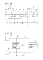
- Figure 11 is a flow chart illustrating production steps of the electrostatic discharge protection device.
- Figure 5 is a cross-sectional view illustrating a step of forming the device separation insulator 3 , Figure 6 a step of forming the n-type well 2 , Figure 7 a step of forming the gate sidewall insulator 12 , Figure 8 a step of patterning a photoresist 26 , Figure 9 a step of depositing a high melting point metal 27 , and Figure 10 a step of forming the silicide layers 10 and 11 .
- the steps illustrated in these figures are those for producing the electrostatic discharge protection device illustrated in Figure 1 .
- the electrostatic discharge protection device illustrated in Figure 2 can be produced in substantially the same way, by substituting the structure of the trigger diode A of Figure 1 (which corresponds to the gate section of a MOS transistor) with the device separation insulator 3 .
- the device separation insulator 3 is formed on the p-type substrate 1 (S101 in Figure 11 ). While the formation of the device separation insulator 3 can be done by any appropriate method, a LOCOS (local oxidation of silicon) method and a shallow trench isolation method are commonly used. Any region not covered with the device separation insulator 3 is covered with a thin oxide film 22 .
- LOCOS local oxidation of silicon
- an n-type well formation photoresist 22 is applied across the entire surface of the wafer, and then patterned by a photolithography process using an n-type well injection photomask. Thereafter, an n-type impurity is injected into the wafer. Then, a p-type impurity may optionally be injected using a p-type well injection photomask, so as to form a p-type well. The photoresist is removed, and a heat treatment is performed to diffuse the n-type impurity so as to form the n-type well 2 (S102 in Figure 11 ).
- the thin oxide film 22 is etched away, and an oxidization process is performed so as to form a gate oxide film 13 of the MOS transistor on the silicon substrate (S103).
- a polysilicon is deposited on the entire surface of the wafer, and a photoresist is applied thereon.
- a photolithography process is performed using a gate formation photomask so as to pattern the photoresist into a gate resist, and a polysilicon etching process is performed so as to pattern the polysilicon 14 on the gate oxide film 13 (S104).
- the photoresist is removed, and an oxidization process is performed so as to grow a thin oxide film across the entire surface.
- a photoresist is applied on the entire surface of the wafer, and a photoresist process is performed using an NMOS transistor LDD implantation mask so as to pattern the photoresist into an NMOS transistor LDD implantation resist. Then, an n-type impurity is implanted into a source/drain region of the NMOS transistor (S105). At this time, a p-type impurity may also be implanted so as to suppress the short channel effect of the NMOS transistor.
- an impurity may be implanted into the n-type anode gate high impurity concentration region 5 , the n-type cathode high impurity concentration region 6 , and the n-type high impurity concentration region 9 of the electrostatic discharge protection device illustrated in Figure 1 or 2 .
- the photoresist is removed, and a photoresist is again applied on the entire surface.
- a photoresist process is performed using a PMOS transistor LDD implantation mask so as to pattern the photoresist into a PMOS transistor LDD implantation resist.
- a p-type impurity is implanted into the source/drain region of the PMOS transistor (S106).
- an n-type impurity may also be implanted so as to suppress the short channel effect of the PMOS transistor.
- an impurity may be implanted into the p-type high impurity concentration region 4 , the p-type cathode gate high impurity concentration region 7 , and the p-type high impurity concentration region 8 of the electrostatic discharge protection device illustrated in Figure 1 or 2 .
- the photoresist is removed, and an oxide film is deposited on the entire surface.
- the surface is subjected to an anisotropic oxide film etching process so as to form the gate sidewall insulator 12 on the sidewall of the polysilicon 14 (S107).
- Thin oxide films 24 and 25 are deposited, and a photoresist is applied on the entire surface.
- a photoresist process is performed using a NMOS transistor source/drain implantation mask so as to pattern the photoresist into an NMOS transistor source/drain implantation photoresist 23 . Then, an n-type impurity is implanted.
- an n-type impurity is implanted into the n-type anode gate high impurity concentration region 5 , the n-type cathode high impurity concentration region 6 , and the n-type high impurity concentration region 9 (S108).
- the photoresist is removed, and a photoresist is applied on the entire surface.
- a photoresist process is performed using a PMOS transistor source/drain implantation mask so as to pattern the photoresist into a PMOS transistor source/drain impurity photoresist 26 .
- a p-type impurity is implanted (Sl10).
- a p-type impurity is implanted into the p-type anode high impurity concentration region 4 , the p-type cathode gate high impurity concentration region 7 , and the p-type high impurity concentration region 8 of the electrostatic discharge protection device illustrated in Figure 1 or 2 (S109).
- the photoresist is removed, and the oxide film on the silicon active region and the oxide film on the polysilicon are removed. Then, the high melting point metal 27 is deposited (S110).
- a heat treatment is performed so as to form the silicide layers 10 and 11 on the surface of the silicon substrate and on the surface of the polysilicon 14 , respectively.
- unreacted high melting point metal is stripped away (S111).
- No silicide layer is formed on the surface of the device separation insulator 3 or on the surface of the gate sidewall insulator 12 . Since no silicide layer is provided on the gate sidewall insulator 12 , the p-type high impurity concentration region 8 and the n-type high impurity concentration region 9 , which together form a trigger diode, will not be electrically shortcircuitted.
- an interlayer insulator is deposited on the entire surface, and the deposited insulator is flattened.
- a photoresist is applied on the entire surface, and patterned into a contact hole opening resist using a contact hole formation photomask.
- the interlayer insulator is etched so as to open contact holes, and then a metal is deposited on the entire surface of the wafer. Then, the metal is patterned using a metal photomask, thereby completing the electrostatic discharge protection device illustrated in Figure 1 or 2 .
- the photomask layout employed for implanting an impurity into the p-type high impurity concentration region and the n-type high impurity concentration region, which together form the trigger diode of the electrostatic discharge protection device, will be described below with reference to Figures 12 to 14 . While the layout described below is an exemplary layout which is suitably used for providing the trigger diode section of the electrostatic discharge protection device, the layout may also be used for providing protection diodes of an electrostatic discharge protection circuit, which will later be further described.
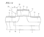
- Figure 12 is a cross-sectional view illustrating an undesirable example of a production step for providing an electrostatic discharge protection device.
- Figure 12 shows an enlarged cross section of the trigger diode section A of the electrostatic discharge protection device illustrated in Figure 1 .
- an n-type high concentration impurity is implanted into a portion of the p-type high impurity concentration region 8 , to be an anode of the trigger diode, thereby forming an n-type impurity region 9a therein.
- n-type impurity region 9a may be formed if the n-type impurity concentration is any higher than the p-type impurity concentration.
- the silicide layer 10 is formed on the surface of the p-type high impurity concentration region 8 and the surface of the n-type impurity region 9a , thereby electrically shortcircuitting the p-type high impurity concentration region 8 and the n-type impurity region 9a with each other. Since the n-type impurity region 9a , the n-type well 2 , and the n-type impurity region 9 are of the same conductivity type, the anode and the cathode of the trigger diode are shortcircuitted with each other.
- the reverse breakdown of the trigger diode will not occur, while the anode gate and the cathode gate of the thyristor, which is an electrostatic discharge protection device comprising a trigger diode, are shortcircuitted with each other.
- a leak current may occur from the anode gate, which is normally at a higher potential, to the cathode gate, which is normally at a reference potential, thereby hampering the normal operation of the semiconductor integrated circuit.
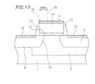
- Figure 13 is a cross-sectional view illustrating a method of providing an electrostatic discharge protection device according to an example of the present invention.
- Figure 13 illustrates a desirable layout of the NMOS transistor source/drain implantation photomask where no shortcircuitting path is formed between the anode and the cathode of the trigger diode.
- an edge 30 of the NMOS transistor source/drain implantation photomask is arranged at a position in the polysilicon region which is shifted toward the cathode from the edge 29 of the gate polysilicon 14 (an edge of the impurity implanted region) by a distance DMAX corresponding to the maximum misalignment of the NMOS transistor source/drain implantation photomask with respect to the gate polysilicon 14 which may possibly occur during the production of a semiconductor integrated circuit. In this way, it is possible to avoid the implantation of an n-type high concentration impurity on the anode side.
- the above-described layout can also be used in the process of forming a protection diode in an n-type substrate or an n-type well which will later be further described with reference to Figure 16 .
- the edge 30 of the NMOS transistor source/drain implantation photomask can be shifted toward the cathode from an edge of the device separation insulator 3 by a distance corresponding to the maximum misalignment which may possibly occur therebetween.
- Figure 14 is an enlarged cross-sectional view illustrating the trigger diode section in the electrostatic discharge protection device illustrated in Figure 3 which is triggered by the breakdown between the n-type high impurity concentration region 9 to be the cathode of the trigger diode and the p-type substrate 1 .
- a p-type high concentration impurity is implanted into the n-type high impurity concentration region 9 during the implantation into the PMOS source/drain region, if the p-type impurity concentration is higher than the n-type impurity concentration, a p-type impurity region is formed in a portion of the n-type high impurity concentration region 9 on the side of the gate 14 .
- the n-type high impurity concentration region 9 , the p-type substrate 1 , and the p-type high impurity concentration region 8 are shortcircuitted with one another by the silicide layer, thereby shortcircuitting the anode and the cathode of the trigger diode.
- Figure 14 is a cross-sectional view illustrating another method of producing an electrostatic discharge protection device according to an example of the present invention.
- Figure 14 illustrates a position of the PMOS transistor source/drain implantation photomask such that no shortcircuitting path is formed between the anode and the cathode of the trigger diode.
- an edge 34 of the PMOS transistor source/drain implantation photomask is arranged at a position in the polysilicon region which is shifted toward the anode from an edge 33 of the gate polysilicon (an edge of the impurity implanted region) by a distance DMAX corresponding to the maximum misalignment of the PMOS transistor source/drain implantation photomask with respect to the gate polysilicon which may possibly occur during the production of a semiconductor integrated circuit. In this way, it is possible to avoid the implantation of a p-type high concentration impurity on the cathode side.
- the above-described layout can also be used in the process of forming a protection diode in a p-type substrate or a p-type well which is illustrated in Figure 17 .
- the edge 34 ( Figure 14 ) of the PMOS transistor source/drain implantation photomask can be shifted toward the cathode from an edge of the device separation insulator 3 by a distance DMAX corresponding to the maximum misalignment which may possibly occur therebetween.
- Figure 15 is a schematic diagram illustrating an electrostatic discharge protection circuit including the electrostatic discharge protection device according to an example of the present invention.
- Figure 15 illustrates an example where the electrostatic discharge protection circuit includes the electrostatic discharge protection device of the present invention between an input/output signal line and a reference voltage line.
- the electrostatic discharge protection circuit includes an electrostatic discharge protection device 39 of the present invention, a protection diode 41 , and a well resistor 46 .
- the anode terminal 36 of the electrostatic discharge protection device 39 is connected to an input/output signal line 43
- a cathode terminal 37 and a cathode gate terminal 38 are connected to a reference voltage line 45 .
- a semiconductor integrated circuit 40a to be electrostatically protected is connected between the input/output signal line 43 and the reference voltage line 45 .
- the well resistor 46 may be made of an n-type well when the semiconductor substrate is of p type, or a p-type well when the semiconductor substrate is of n type.
- the protection diode 41 is provided in the step of producing the electrostatic discharge protection device 39 .
- the protection diode 41 includes the p-type anode high impurity concentration region 8 ( Figure 1 ) and the n-type cathode high impurity concentration region 9 provided in a p-type or n
- Figure 16 is a cross-sectional view illustrating an example of the protection diode 41 (Figure 15 ) provided in the electrostatic discharge protection circuit of the present invention.
- Figure 17 is a cross-sectional view illustrating another example of the protection diode 41 ( Figure 15 ) provided in the electrostatic discharge protection circuit of the present invention.
- the protection diode 41 is provided on a p-type substrate 1 .
- the anode and the cathode are insulated from each other by a gate structure (including the gate sidewall insulator 12 , the gate oxide film 13 , and the polysilicon 14 ) so as to prevent the p-type anode high impurity concentration region 8 and the n-type cathode high impurity concentration region 9 from being shortcircuitted with each other by a silicide layer.
- the insulation between the p-type anode high impurity concentration region 8 and the n-type cathode high impurity concentration region 9 may alternatively be provided by using the device separation insulator 3 , as in the trigger diode A of Figure 2 .
- the n-type cathode high impurity concentration region 9 of the protection diode 41 is connected to the input/output signal line 43 , and the anode 8 is connected to the reference voltage line 45 .
- the diode in the electrostatic discharge protection device 39 (including the p-type cathode gate high impurity concentration region 7 , the p-type substrate 1 , the n-type well 2 , and the n-type anode gate high impurity concentration region 5 ) is biased in the forward direction, while the protection diode 41 is also biased in the forward direction. Therefore, the positive electrostatic charge entering through the reference voltage terminal 44 can be bypassed to the input/output signal line 43 and to the input/output terminal 42 .
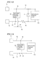
- Figure 18 is a schematic diagram illustrating another example of an electrostatic discharge protection circuit including the electrostatic discharge protection device according to an example of the present invention.
- Figure 18 illustrates an example where an electrostatic discharge protection circuit is provided between a voltage supply line and an input/output signal line by using the electrostatic discharge protection device 39 of the present invention.
- the electrostatic discharge protection circuit includes the electrostatic discharge protection device 39 of the present invention, the protection diode 41 , and the well resistor 46 .
- the anode terminal 36 of the electrostatic discharge protection device 39 is connected to a power supply line 52 , the cathode terminal 37 to the input/output signal line 43 , and the cathode gate terminal 38 to the reference voltage line 45 .
- a semiconductor integrated circuit 40b to be electrostatically protected is connected between the power supply line 52 and the input/output signal line 43 .
- the protection diode 41 is provided in the step of producing the electrostatic discharge protection device 39.
- the protection diode 41 includes the p-type anode high impurity concentration region 8 ( Figure 17 ) and the n-type cathode high impurity concentration region 9 provided in an n-type well.
- Figure 17 illustrates an example of the protection diode 41 provided in the n-type well 2 on the p-type substrate 1.
- the n-type cathode high impurity concentration region 9 of the protection diode 41 is connected to the power supply line 52
- the p-type anode high impurity concentration region 8 is connected to the input/output signal line 43.
- the protection diode 41 When a positive electrostatic charge flows into the circuit through the input/output terminal 42 , the protection diode 41 is biased in the forward direction. Therefore, the positive electrostatic charge entering through the input/output terminal 42 can be bypassed to the power supply line 52 .
- Figure 19 is a schematic diagram illustrating another example of an electrostatic discharge protection circuit provided between the voltage supply line and the reference voltage line using the electrostatic discharge protection device according to an example of the present invention.
- the anode terminal 36 of the electrostatic discharge protection device is connected to the power supply line 52 , and the cathode terminal 37 and the cathode gate terminal 38 are connected to the reference voltage line 45 .
- a semiconductor integrated circuit 40c to be electrostatically protected is connected between the power supply line 52 and the reference voltage line 45 .
- the diode in the electrostatic discharge protection device 39 (including the p-type cathode gate high impurity concentration region 7 , the p-type substrate 1 , the n-type well 2 , and the n-type anode gate high impurity concentration region 5 ( Figure 1 )) is biased in the forward direction. Therefore, the positive electrostatic charge entering through the reference voltage terminal 44 can be bypassed to the power supply line 52 and to the power supply terminal 51 .
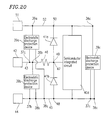
- Figure 20 is a schematic diagram illustrating an electrostatic discharge protection circuit including the electrostatic discharge protection device as described above according to an example of the present invention, which is capable of bypassing an electrostatic charge entering the semiconductor integrated circuit through any of an input/output terminal, a power supply terminal, and a reference voltage terminal, to another of the input/output terminal, the power supply terminal, and the reference voltage terminal.
- the electrostatic discharge protection circuit comprises electrostatic discharge protection devices 39a, 39b and 39c according to the present invention, protection diodes 41a and 41b , and a well resistor 46 .
- An anode terminal 36a of the electrostatic discharge protection device 39a is connected to the power supply line 52 , a cathode terminal 37a thereof to the input/output signal line 43 , and a cathode gate terminal 38a thereof to the reference voltage line 45 .
- An anode terminal 36b of the electrostatic discharge protection device 39b is connected to the input/output signal line 43 , a cathode terminal 37b and a cathode gate terminal 38b thereof to the reference voltage line 45 .
- An anode terminal 36c of the electrostatic discharge protection device 39c is connected to the power supply line 52 , and a cathode terminal 37c and a cathode gate terminal 38c to the reference voltage line 45.
- a semiconductor integrated circuit 40d to be electrostatically protected is connected between the power supply line 52 and the reference voltage line 45 .
- the protection diodes 41a and 41b are provided in the step of producing the electrostatic discharge protection devices 39a, 39b and 39c .
- the protection diode 41a includes the p-type anode high impurity concentration region 8 and the n-type cathode high impurity concentration region 9 .
- An example of this is the protection diode formed in the n-type well 2 on the p-type substrate 1 as illustrated in Figure 17 .
- the p-type anode high impurity concentration region 8 of the protection diode 41a is connected to the input/output signal line 43 , and the n-type cathode high impurity concentration region 9 thereof is connected to the power supply line 52 .
- the protection diode 41b includes the p-type anode high impurity concentration region 8 and the n-type cathode high impurity concentration region 9 .
- An example of such a diode is the protection diode formed on the p-type substrate 1 illustrated in Figure 16 .
- the p-type anode high impurity concentration region 8 of the protection diode 41b is connected to the reference voltage line 45
- the n-type cathode high impurity concentration region 9 is connected to the input/output signal line 43.
- the diode in the electrostatic discharge protection device 39b (including the p-type cathode gate high impurity concentration region 7 , the p-type substrate 1, the n-type well 2 , and the n-type anode gate high impurity concentration region 5 ( Figure 1 )) is biased in the forward direction, while the protection diode 41b is also biased in the forward direction. Therefore, the positive electrostatic charge entering through the reference voltage terminal 44 can be bypassed to the input/output signal line 43 through the low-resistance bypass.
- the power supply line 52 When a positive electrostatic charge flows into the circuit through the power supply terminal 51 and the reference voltage terminal is grounded, the power supply line 52 is brought to a higher voltage than the reference voltage line 45 , thereby turning ON the electrostatic discharge protection device 39c while forming a low-resistance bypass between the power supply line 52 and the reference voltage line 45 .
- the electrostatic charge entering through the power supply terminal 51 can be bypassed to the reference voltage line 45 through the electrostatic discharge protection device 39c.
- the diode in the electrostatic discharge protection device 39c (including the p-type cathode gate high impurity concentration region 7 , the p-type substrate 1 , the n-type well 2 , and the n-type anode gate high impurity concentration region 5 ( Figure 1)) is biased in the forward direction, while the protection diodes 41a and 41b are connected in series in the forward direction. Therefore, the positive electrostatic charge entering through the reference voltage terminal 44 can be bypassed to the power supply line 52 and the power supply terminal 51 through the low-resistance bypass.
- Figure 21 is a schematic diagram illustrating an electrostatic discharge protection circuit including the electrostatic discharge protection device as described above according to another example of the present invention, which is capable of bypassing an electrostatic charge entering the semiconductor integrated circuit through any of an input/output terminal, a power supply terminal, and a reference voltage terminal, to another of the input/output terminal, the power supply terminal, and the reference voltage terminal.
- the electrostatic discharge protection circuit of Figure 21 is obtained by eliminating the protection diodes 41a and 41b from the electrostatic discharge protection circuit of Figure 20 .
- a voltage equal to or greater than the breakdown voltage between the protection diodes 41a and 41b may be applied to the semiconductor integrated circuit 40d .
- the electrostatic discharge protection circuit of Figure 21 may be employed to implement an electrostatic discharge protection circuit capable of bypassing an electrostatic charge entering through any of an input/output terminal, a power supply terminal, and a reference voltage terminal, to another of the input/output terminal, the power supply terminal, and the reference voltage terminal, as will be described in more detail below.
- a positive electrostatic charge entering the circuit of Figure 21 through the input/output terminal 42 can be bypassed to the power supply terminal 51 through a low-resistance electrostatic charge bypass, which extends from the input/output terminal 42 , via the input/output signal line 43 , the electrostatic discharge protection device 39b , the reference voltage line 45 , the forward diode of the electrostatic discharge protection device 39c (including the p-type cathode gate high impurity concentration region 7 , the p-type substrate 1 , the n-type well 2 , and the n-type anode gate high impurity concentration region 5 ( Figure 1 )), the power supply line 52 , and then to power supply terminal 51 .
- a low-resistance electrostatic charge bypass which extends from the input/output terminal 42 , via the input/output signal line 43 , the electrostatic discharge protection device 39b , the reference voltage line 45 , the forward diode of the electrostatic discharge protection device 39c (including the p-type ca
- a positive electrostatic charge entering the circuit of Figure 21 through the input/output terminal 42 can be bypassed to the reference voltage terminal 44 through a low-resistance electrostatic charge bypass, which extends from the input/output terminal 42 , via the input/output signal line 43 , the electrostatic discharge protection device 39b , the reference voltage line 45 , and then to the reference voltage terminal 44 .
- a positive electrostatic charge entering the circuit of Figure 21 through the power supply terminal 51 can be bypassed to the input/output terminal 42 through a low-resistance electrostatic charge bypass, which extends from the power supply terminal 51 , via the power supply line 52 , the electrostatic discharge protection device 39a, the input/output signal line 43 , and then to the input/output terminal 42 .
- a positive electrostatic charge entering the circuit of Figure 21 through the power supply terminal 51 can be bypassed to the reference voltage terminal 44 through a low-resistance electrostatic charge bypass, which extends from the power supply terminal 51 , via the power supply line 52 , the electrostatic discharge protection device 39c , the reference voltage line 45 , and then to the reference voltage terminal 44.
- a positive electrostatic charge entering the circuit of Figure 21 through the reference voltage terminal 44 can be bypassed to the input/output terminal 42 through a low-resistance electrostatic charge bypass, which extends from the reference voltage terminal 44 , via the forward diode of the electrostatic discharge protection device 39b (including the p-type cathode gate high impurity concentration region 7 , the p-type substrate 1 , the n-type well 2 , and the n-type anode gate high impurity concentration region 5 ( Figure 1 )), the input/output signal line 43 , and then to the input/output terminal 42 .
- a low-resistance electrostatic charge bypass which extends from the reference voltage terminal 44 , via the forward diode of the electrostatic discharge protection device 39b (including the p-type cathode gate high impurity concentration region 7 , the p-type substrate 1 , the n-type well 2 , and the n-type anode gate high impurity concentration region 5 ( Figure 1
- a positive electrostatic charge entering the circuit of Figure 21 through the reference voltage terminal 44 can be bypassed to the power supply terminal 51 through a low-resistance electrostatic charge bypass, which extends from the reference voltage terminal 44 , via the reference voltage line 45 , the forward diode of the electrostatic discharge protection device 39c (including the p-type cathode gate high impurity concentration region 7 , the p-type substrate 1 , the n-type well 2 , and the n-type anode gate high impurity concentration region 5 ( Figure 1 )), the power supply line 52 , and then to the power supply terminal 51 .
- a low-resistance electrostatic charge bypass which extends from the reference voltage terminal 44 , via the reference voltage line 45 , the forward diode of the electrostatic discharge protection device 39c (including the p-type cathode gate high impurity concentration region 7 , the p-type substrate 1 , the n-type well 2 , and the n-type anode gate high impurity
- the semiconductor integrated circuit 40d is not broken by an applied voltage which is equal to or greater than the breakdown voltage between the protection diodes 41a and 41b, it is possible, by employing the electrostatic discharge protection circuit of Figure 21 , to eliminate one or more protection diodes, thereby reducing the layout area occupied by the electrostatic discharge protection circuit, and thus reducing the area of the chip on which the semiconductor integrated circuit is to be provided. Therefore, it is possible to increase the number of semiconductor integrated circuit chips to be fabricated on a wafer, thereby providing an effect of reducing the cost of a semiconductor integrated circuit chip. While the well resistor 46 is provided in the above examples for restricting the electrostatic charge flowing into the semiconductor integrated circuit 40d , the well resistor 46 may be eliminated in some cases where the electrostatic resistance of the semiconductor integrated circuit 40d is relatively high.
- Figure 22 is a schematic diagram illustrating an electrostatic discharge protection circuit including the electrostatic discharge protection device as described above according to another example of the present invention, which is capable of bypassing an electrostatic charge entering the semiconductor integrated circuit through any of an input/output terminal, a power supply terminal, and a reference voltage terminal, to another of the input/output terminal, the power supply terminal, and the reference voltage terminal.
- the electrostatic discharge protection circuit of Figure 22 is obtained by eliminating the electrostatic discharge protection device 39a and the protection diode 41a from the electrostatic discharge protection circuit of Figure 22.
- the electrostatic discharge protection circuit of Figure 22 may be employed to implement an electrostatic discharge protection circuit capable of bypassing an electrostatic charge entering through any of an input/output terminal, a power supply terminal, and a reference voltage terminal, to another of the input/output terminal, the power supply terminal, and the reference voltage terminal, as will be described in more detail below.
- a positive electrostatic charge entering the circuit of Figure 22 through the input/output terminal 42 can be bypassed to the power supply terminal 51 through a low-resistance electrostatic charge bypass, which extends from the input/output terminal 42 , via the input/output signal line 43 , the electrostatic discharge protection device 39b , the reference voltage line 45 , the forward diode of the electrostatic discharge protection device 39c (including the p-type cathode gate high impurity concentration region 7 , the p-type substrate 1 , the n-type well 2 , and the n-type anode gate high impurity concentration region 5 ( Figure 1 )), the power supply line 52, and then to power supply terminal 51 .
- a low-resistance electrostatic charge bypass which extends from the input/output terminal 42 , via the input/output signal line 43 , the electrostatic discharge protection device 39b , the reference voltage line 45 , the forward diode of the electrostatic discharge protection device 39c (including the p-type cath
- a positive electrostatic charge entering the circuit of Figure 22 through the input/output terminal 42 can be bypassed to the reference voltage terminal 44 through a low-resistance electrostatic charge bypass, which extends from the input/output terminal 42 , via the input/output signal line 43 , the electrostatic discharge protection device 39b , the reference voltage line 45 , and then to the reference voltage terminal 44.
- a positive electrostatic charge entering the circuit of Figure 22 through the power supply terminal 51 can be bypassed to the input/output terminal 42 through a low-resistance electrostatic charge bypass, which extends from the power supply terminal 51 , via the power supply line 52 , the electrostatic discharge protection device 39c , the reference voltage line 45 , the protection diode 41b , the forward diode of the electrostatic discharge protection device 39b (including the p-type cathode gate high impurity concentration region 7 , the p-type substrate 1 , the n-type well 2 , and the n-type anode gate high impurity concentration region 5 ( Figure 1 )), the input/output signal line 43, and then to the input/output terminal 42 .
- a low-resistance electrostatic charge bypass which extends from the power supply terminal 51 , via the power supply line 52 , the electrostatic discharge protection device 39c , the reference voltage line 45 , the protection diode 41b , the forward diode of the electrostatic
- a positive electrostatic charge entering the circuit of Figure 22 through the power supply terminal 51 can be bypassed to the reference voltage terminal 44 through a low-resistance electrostatic charge bypass, which extends from the power supply terminal 51 , via the power supply line 52 , the electrostatic discharge protection device 39c , the reference voltage line 45 , and then to the reference voltage terminal 44 .
- a positive electrostatic charge entering the circuit of Figure 22 through the reference voltage terminal 44 can be bypassed to the input/output terminal 42 through a low-resistance electrostatic charge bypass, which extends from the reference voltage terminal 44 , via the forward diode of the electrostatic discharge protection device 39b (including the p-type cathode gate high impurity concentration region 7 , the p-type substrate 1 , the n-type well 2 , and the n-type anode gate high impurity concentration region 5 ( Figure 1 )), the protection diode 41b , the input/output signal line 43 , and then to the input/output terminal 42 .
- the electrostatic discharge protection device 39b including the p-type cathode gate high impurity concentration region 7 , the p-type substrate 1 , the n-type well 2 , and the n-type anode gate high impurity concentration region 5 ( Figure 1 )
- a positive electrostatic charge entering the circuit of Figure 22 through the reference voltage terminal 44 can be bypassed to the power supply terminal 51 through a low-resistance electrostatic charge bypass, which extends from the reference voltage terminal 44 , via the reference voltage line 45, the forward diode of the electrostatic discharge protection device 39c (including the p-type cathode gate high impurity concentration region 7 , the p-type substrate 1 , the n-type well 2 , and the n-type anode gate high impurity concentration region 5 ), the power supply line 52 , and then to the power supply terminal 51 .
- a low-resistance electrostatic charge bypass which extends from the reference voltage terminal 44 , via the reference voltage line 45, the forward diode of the electrostatic discharge protection device 39c (including the p-type cathode gate high impurity concentration region 7 , the p-type substrate 1 , the n-type well 2 , and the n-type anode gate high impurity concentration region 5 ), the
- an excessive voltage which is equal to or greater than the breakdown voltage of the protection diode 41a may be applied for a short period of time to the semiconductor integrated circuit 40d between a contact 58 (between the semiconductor integrated circuit 40d and the power supply line 52 ) and another contact 59 (between the semiconductor integrated circuit 40d and the input/output signal line 43 ).
- the semiconductor integrated circuit 40d has a sufficient resistance against the short-time application of an excessive voltage which is as high as the turn-on voltage of the electrostatic discharge protection devices 39b or 39c , the elimination of the electrostatic discharge protection device 39a and the protection diode 41a provides an effect of reducing the layout area occupied by the electrostatic discharge protection circuit, and thus reducing the area of the chip on which the semiconductor integrated circuit is to be provided. Therefore, there is provided an effect of reducing the cost of a semiconductor integrated circuit chip. While the well resistor 46 is provided in the above examples for restricting the electrostatic charge flowing into the semiconductor integrated circuit 40d , the well resistor 46 may be eliminated in some cases where the electrostatic resistance of the semiconductor integrated circuit 40d is relatively high.
- Figure 23 is a schematic diagram illustrating an electrostatic discharge protection circuit including the electrostatic discharge protection device as described above according to another example of the present invention, which is capable of bypassing an electrostatic charge entering the semiconductor integrated circuit through any of an input/output terminal, a power supply terminal, and a reference voltage terminal, to another of the input/output terminal, the power supply terminal, and the reference voltage terminal.
- the electrostatic discharge protection circuit of Figure 23 is obtained by further eliminating the protection diode 41b from the electrostatic discharge protection circuit of Figure 22 .
- a positive electrostatic charge entering the circuit of Figure 23 through the input/output terminal 42 can be bypassed to the power supply terminal 51 through a low-resistance electrostatic charge bypass, which extends from the input/output terminal 42 , via the input/output signal line 43 , the electrostatic discharge protection device 39b, the reference voltage line 45 , the forward diode of the electrostatic discharge protection device 39c (including the p-type cathode gate high impurity concentration region 7 , the p-type substrate 1 , the n-type well 2 , and the n-type anode gate high impurity concentration region 5 ( Figure 1 )), the power supply line 52 , and then to power supply terminal 51.
- a low-resistance electrostatic charge bypass which extends from the input/output terminal 42 , via the input/output signal line 43 , the electrostatic discharge protection device 39b, the reference voltage line 45 , the forward diode of the electrostatic discharge protection device 39c (including the p-type cathode
- a positive electrostatic charge entering the circuit of Figure 23 through the input/output terminal 42 can be bypassed to the reference voltage terminal 44 through a low-resistance electrostatic charge bypass, which extends from the input/output terminal 42 , via the input/output signal line 43 , the electrostatic discharge protection device 39b , the reference voltage line 45 , and then to the reference voltage terminal 44 .
- a positive electrostatic charge entering the circuit of Figure 23 through the power supply terminal 51 can be bypassed to the input/output terminal 42 through a low-resistance electrostatic charge bypass, which extends from the power supply terminal 51 , via the power supply line 52 , the electrostatic discharge protection device 39c , the reference voltage line 45 , the forward diode of the electrostatic discharge protection device 39b (including the p-type cathode gate high impurity concentration region 7 , the p-type substrate 1 , the n-type well 2 , and the n-type anode gate high impurity concentration region 5 ( Figure 1 )), the input/output signal line 43 , and then to the input/output terminal 42 .
- a low-resistance electrostatic charge bypass which extends from the power supply terminal 51 , via the power supply line 52 , the electrostatic discharge protection device 39c , the reference voltage line 45 , the forward diode of the electrostatic discharge protection device 39b (including the p-type cathode gate
- a positive electrostatic charge entering the circuit of Figure 23 through the power supply terminal 51 can be bypassed to the reference voltage terminal 44 through a low-resistance electrostatic charge bypass, which extends from the power supply terminal 51 , via the power supply line 52 , the electrostatic discharge protection device 39c , the reference voltage line 45 , and then to the reference voltage terminal 44.
- a positive electrostatic charge entering the circuit of Figure 23 through the reference voltage terminal 44 can be bypassed to the input/output terminal 42 through a low-resistance electrostatic charge bypass, which extends from the reference voltage terminal 44 , via the forward diode of the electrostatic discharge protection device 39b (including the p-type cathode gate high impurity concentration region 7 , the p-type substrate 1 , the n-type well 2 , and the n-type anode gate high impurity concentration region 5 ( Figure 1 )), the input/output signal line 43 , and then to the input/output terminal 42 .
- a low-resistance electrostatic charge bypass which extends from the reference voltage terminal 44 , via the forward diode of the electrostatic discharge protection device 39b (including the p-type cathode gate high impurity concentration region 7 , the p-type substrate 1 , the n-type well 2 , and the n-type anode gate high impurity concentration region 5 ( Figure 1
- a positive electrostatic charge entering the circuit of Figure 23 through the reference voltage terminal 44 can be bypassed to the power supply terminal 51 through a low-resistance electrostatic charge bypass, which extends from the reference voltage terminal 44, via the reference voltage line 45 , the forward diode of the electrostatic discharge protection device 39c (including the p-type cathode gate high impurity concentration region 7 , the p-type substrate 1 , the n-type well 2 , and the n-type anode gate high impurity concentration region 5 ( Figure 1 )), the power supply line 52 , and then to the power supply terminal 51 .
- a low-resistance electrostatic charge bypass which extends from the reference voltage terminal 44, via the reference voltage line 45 , the forward diode of the electrostatic discharge protection device 39c (including the p-type cathode gate high impurity concentration region 7 , the p-type substrate 1 , the n-type well 2 , and the n-type anode gate high impurity concentration region
- an excessive voltage which is equal to or greater than the breakdown voltage of the protection diode 41b may be applied for a short period of time to the semiconductor integrated circuit 40d between a contact 60 (between the semiconductor integrated circuit 40d and the reference voltage line 45) and the contact 59 (between the semiconductor integrated circuit 40d and the input/output signal line 43 ).
- the elimination of the protection diode 41b of Figure 22 provides an effect of reducing the layout area occupied by the electrostatic discharge protection circuit, and thus reduces the area of the chip on which the semiconductor integrated circuit is to be provided. Therefore, there is provided an effect of reducing the cost of a semiconductor integrated circuit chip.
- the well resistor 46 is provided in the above examples for restricting the electrostatic charge flowing into the semiconductor integrated circuit 40d , the well resistor 46 may be eliminated in some cases where the electrostatic resistance of the semiconductor integrated circuit 40d is relatively high.
- the thyristor structure including the trigger diode of the present invention it is possible to provide an electrostatic discharge protection device which can be turned ON by a low voltage less than or equal to the breakdown voltage between an n-type well and a p-type substrate (or a p-type well), or the breakdown voltage between a p-type well and an n-type substrate (or an n-type well).
- an electrostatic discharge protection device which can desirably prevent breaking of the semiconductor integrated circuit due to the electrostatic discharge phenomenon.
- Even when a salicide step is employed in the production of the semiconductor integrated circuit the p-type high impurity concentration region and the n-type high impurity concentration region of the trigger diode can be insulated from each other. Therefore, it is possible to prevent the anode and the cathode of the thyristor from being electrically shortcircuitted with each other and thereby hampering the normal operation of the semiconductor integrated circuit.
- the layout of a p-type or n-type high concentration ion implantation mask according to the present invention is employed in the production of a trigger diode or a protection diode, it is possible to prevent the cathode and the anode of the diode from being electrically shortcircuitted with each other and thereby producing a leak current in the semiconductor integrated circuit, which may otherwise occur when a salicide step is employed in the process of producing a semiconductor integrated circuit.
- an electrostatic discharge protection circuit including the electrostatic discharge protection device of the present invention, it is possible to provide an electrostatic bypass between a power supply line and an input/output signal line, between a reference voltage line and an input/output signal line, or between a power supply line and a reference voltage line.
- a semiconductor integrated circuit which is connected between the power supply line and the input/output signal line, between the reference voltage line and the input/output signal line, or between the power supply line and the reference voltage line, from breaking due to the electrostatic discharge phenomenon.
- one or more of the electrostatic discharge protection devices forming the electrostatic discharge protection circuit and/or one or more of the protection diodes may be eliminated depending upon the electrostatic breakdown resistance of the semiconductor integrated circuit against an electrostatic charge flowing into/out of the circuit and/or depending upon the desired electrostatic breakdown resistance.
Landscapes
- Engineering & Computer Science (AREA)
- Power Engineering (AREA)
- Microelectronics & Electronic Packaging (AREA)
- Physics & Mathematics (AREA)
- Condensed Matter Physics & Semiconductors (AREA)
- General Physics & Mathematics (AREA)
- Computer Hardware Design (AREA)
- Ceramic Engineering (AREA)
- Semiconductor Integrated Circuits (AREA)
- Metal-Oxide And Bipolar Metal-Oxide Semiconductor Integrated Circuits (AREA)
- Thyristors (AREA)
Applications Claiming Priority (4)
| Application Number | Priority Date | Filing Date | Title |
|---|---|---|---|
| JP23917098 | 1998-08-25 | ||
| JP23917098 | 1998-08-25 | ||
| JP23095599A JP4256544B2 (ja) | 1998-08-25 | 1999-08-17 | 半導体集積回路の静電気保護装置、その製造方法および静電気保護装置を用いた静電気保護回路 |
| JP23095599 | 1999-08-17 |
Publications (3)
| Publication Number | Publication Date |
|---|---|
| EP0982776A2 true EP0982776A2 (fr) | 2000-03-01 |
| EP0982776A3 EP0982776A3 (fr) | 2000-11-02 |
| EP0982776B1 EP0982776B1 (fr) | 2008-04-16 |
Family
ID=26529623
Family Applications (1)
| Application Number | Title | Priority Date | Filing Date |
|---|---|---|---|
| EP99306769A Expired - Lifetime EP0982776B1 (fr) | 1998-08-25 | 1999-08-25 | Thyristor de protection ESD avec diode de déclenchement |
Country Status (6)
| Country | Link |
|---|---|
| US (3) | US6338986B1 (fr) |
| EP (1) | EP0982776B1 (fr) |
| JP (1) | JP4256544B2 (fr) |
| KR (1) | KR100325553B1 (fr) |
| DE (1) | DE69938523T2 (fr) |
| TW (1) | TW441124B (fr) |
Cited By (2)
| Publication number | Priority date | Publication date | Assignee | Title |
|---|---|---|---|---|
| GB2368975A (en) * | 2000-08-11 | 2002-05-15 | Samsung Electronics Co Ltd | Protection device with a silicon-controlled rectifier |
| CN103681651A (zh) * | 2012-09-07 | 2014-03-26 | 旺宏电子股份有限公司 | 静电放电保护电路装置 |
Families Citing this family (39)
| Publication number | Priority date | Publication date | Assignee | Title |
|---|---|---|---|---|
| JP4256544B2 (ja) | 1998-08-25 | 2009-04-22 | シャープ株式会社 | 半導体集積回路の静電気保護装置、その製造方法および静電気保護装置を用いた静電気保護回路 |
| JP3810246B2 (ja) * | 2000-03-15 | 2006-08-16 | 株式会社ルネサステクノロジ | 半導体装置および半導体装置の製造方法 |
| DE10022367C2 (de) * | 2000-05-08 | 2002-05-08 | Micronas Gmbh | ESD-Schutzstruktur und Verfahren zur Herstellung |
| JP3675303B2 (ja) | 2000-05-31 | 2005-07-27 | セイコーエプソン株式会社 | 静電気保護回路が内蔵された半導体装置及びその製造方法 |
| US6376342B1 (en) * | 2000-09-27 | 2002-04-23 | Vanguard International Semiconductor Corporation | Method of forming a metal silicide layer on a source/drain region of a MOSFET device |
| US7142296B2 (en) * | 2000-10-30 | 2006-11-28 | Sru Biosystems, Inc. | Method and apparatus for detecting biomolecular interactions |
| US6521487B1 (en) * | 2001-12-05 | 2003-02-18 | United Microelectronics Corp. | Method for making a thyristor |
| JP4146672B2 (ja) * | 2002-06-14 | 2008-09-10 | シャープ株式会社 | 静電気保護素子 |
| US20030230631A1 (en) * | 2002-06-17 | 2003-12-18 | Hitachi, Ltd. | IC card |
| US7265740B2 (en) * | 2002-08-30 | 2007-09-04 | Toshiba Matsushita Display Technology Co., Ltd. | Suppression of leakage current in image acquisition |
| JP2004296883A (ja) * | 2003-03-27 | 2004-10-21 | Sharp Corp | 半導体装置とその製造方法 |
| US20050212051A1 (en) * | 2003-04-16 | 2005-09-29 | Sarnoff Corporation | Low voltage silicon controlled rectifier (SCR) for electrostatic discharge (ESD) protection of silicon-on-insulator technologies |
| US7164185B1 (en) * | 2004-02-02 | 2007-01-16 | Advanced Micro Devices, Inc. | Semiconductor component and method of manufacture |
| JP4996057B2 (ja) * | 2004-05-26 | 2012-08-08 | 旭化成エレクトロニクス株式会社 | 半導体回路 |
| WO2005124883A1 (fr) * | 2004-06-22 | 2005-12-29 | Aruze Corp. | Dispositif thermoélectrique |
| US7420250B2 (en) * | 2004-08-30 | 2008-09-02 | Taiwan Semiconductor Manufacturing Company, Ltd. | Electrostatic discharge protection device having light doped regions |
| KR100629436B1 (ko) * | 2004-09-08 | 2006-09-27 | 매그나칩 반도체 유한회사 | 고전압 소자의 정전기 보호장치 |
| JP4282581B2 (ja) * | 2004-09-29 | 2009-06-24 | 株式会社東芝 | 静電保護回路 |
| US7880223B2 (en) * | 2005-02-11 | 2011-02-01 | Alpha & Omega Semiconductor, Ltd. | Latch-up free vertical TVS diode array structure using trench isolation |
| KR100689884B1 (ko) * | 2005-02-15 | 2007-03-09 | 삼성전자주식회사 | 쇼트키 다이오드를 이용한 노이즈 제거를 위한 반도체 소자및 그 제조방법 |
| US9165920B2 (en) * | 2005-10-15 | 2015-10-20 | Globalfoundries Singapore Pte. Ltd. | Tunable protection system for integrated circuits |
| KR100713935B1 (ko) * | 2006-04-14 | 2007-05-07 | 주식회사 하이닉스반도체 | 반도체 메모리 장치의 정전기 방전 보호 회로 및 정전기방전 보호 방법 |
| US20070257326A1 (en) * | 2006-05-08 | 2007-11-08 | Chien-Li Kuo | Integrated circuit structure and method of manufacturing a memory cell |
| US7609495B2 (en) * | 2006-10-31 | 2009-10-27 | Infineon Technologies Ag | Electrostatic discharge (ESD) protection arrangement and ESD protection method |
| US9202938B2 (en) * | 2006-11-30 | 2015-12-01 | Alpha And Omega Semiconductor Incorporated | Latch-up free vertical TVS diode array structure using trench isolation |
| JP4245644B1 (ja) * | 2007-11-21 | 2009-03-25 | シャープ株式会社 | 静電気放電保護装置及びこれを備えた半導体集積回路 |
| JP5728171B2 (ja) | 2009-06-29 | 2015-06-03 | 株式会社半導体エネルギー研究所 | 半導体装置 |
| JP2012004456A (ja) * | 2010-06-18 | 2012-01-05 | Sony Corp | 半導体装置 |
| TWI424544B (zh) * | 2011-03-31 | 2014-01-21 | Novatek Microelectronics Corp | 積體電路裝置 |
| US8809905B2 (en) * | 2011-12-28 | 2014-08-19 | Taiwan Semiconductor Manufacturing Company, Ltd. | Vertical BJT and SCR for ESD |
| US9117673B2 (en) * | 2012-09-04 | 2015-08-25 | Macronix International Co., Ltd. | Electrostatic discharge protection circuit including a plurality of doped regions and a gate connected to a capacitor and a resistor |
| TWI645534B (zh) * | 2015-03-06 | 2018-12-21 | 聯華電子股份有限公司 | 半導體靜電放電保護元件 |
| US10562123B2 (en) * | 2015-06-18 | 2020-02-18 | Illinois Tool Works Inc. | Welding system with arc control |
| US11335674B2 (en) | 2019-06-27 | 2022-05-17 | Globalfoundries U.S. Inc. | Diode triggered silicon controlled rectifier (SCR) with hybrid diodes |
| US11430881B2 (en) * | 2020-03-05 | 2022-08-30 | Globalfoundries U.S. Inc. | Diode triggered compact silicon controlled rectifier |
| CN113540070B (zh) * | 2020-04-20 | 2023-12-12 | 长鑫存储技术有限公司 | 静电保护电路 |
| CN113070571B (zh) * | 2021-03-18 | 2022-07-19 | 苏州方林科技股份有限公司 | 一种热保护器的自动复位焊接装置及其工艺 |
| CN114122111B (zh) * | 2022-01-26 | 2022-05-03 | 江苏游隼微电子有限公司 | 一种具有寄生二极管的mos栅控晶闸管及制备方法 |
| US11935946B2 (en) * | 2022-06-27 | 2024-03-19 | Globalfoundries U.S. Inc. | Silicon-controlled rectifiers in a silicon-on-insulator technology |
Citations (5)
| Publication number | Priority date | Publication date | Assignee | Title |
|---|---|---|---|---|
| US4331884A (en) * | 1979-04-03 | 1982-05-25 | Asea Aktiebolag | Two-pole overcurrent protection device |
| US4694315A (en) * | 1985-02-26 | 1987-09-15 | Asea Aktiebolag | CMOS overvoltage protection circuit utilizing thyristor and majority carrier injecting anti-parallel diode |
| US5274262A (en) * | 1989-05-17 | 1993-12-28 | David Sarnoff Research Center, Inc. | SCR protection structure and circuit with reduced trigger voltage |
| US5602404A (en) * | 1995-01-18 | 1997-02-11 | National Semiconductor Corporation | Low voltage triggering silicon controlled rectifier structures for ESD protection |
| US5708550A (en) * | 1995-10-25 | 1998-01-13 | David Sarnoff Research Center, Inc. | ESD protection for overvoltage friendly input/output circuits |
Family Cites Families (14)
| Publication number | Priority date | Publication date | Assignee | Title |
|---|---|---|---|---|
| JPH02106766A (ja) * | 1988-10-17 | 1990-04-18 | Hitachi Ltd | 静電記録ヘッド、画像記録装置、現像剤供給装置、ディスプレイ装置、及び静電記録ヘッドの製造方法 |
| US5210846B1 (en) * | 1989-05-15 | 1999-06-29 | Dallas Semiconductor | One-wire bus architecture |
| US5072273A (en) | 1990-05-04 | 1991-12-10 | David Sarnoff Research Center, Inc. | Low trigger voltage SCR protection device and structure |
| JP2794499B2 (ja) * | 1991-03-26 | 1998-09-03 | 株式会社半導体エネルギー研究所 | 半導体装置の作製方法 |
| JP3375659B2 (ja) * | 1991-03-28 | 2003-02-10 | テキサス インスツルメンツ インコーポレイテツド | 静電放電保護回路の形成方法 |
| EP0517391A1 (fr) * | 1991-06-05 | 1992-12-09 | STMicroelectronics, Inc. | Circuit de protection ESD |
| JPH05315552A (ja) * | 1992-05-14 | 1993-11-26 | Nissan Motor Co Ltd | 半導体保護装置 |
| EP0700089A1 (fr) * | 1994-08-19 | 1996-03-06 | STMicroelectronics S.r.l. | Dispositif de protection contre des décharges électrostatiques sur les bornes d'entrée/sortie d'un circuit intégré MOS |
| JP2850801B2 (ja) * | 1995-07-28 | 1999-01-27 | 日本電気株式会社 | 半導体素子 |
| US6108181A (en) * | 1996-04-23 | 2000-08-22 | Motorola Inc. | Electrostatic discharge (ESD) circuit |
| US5825600A (en) * | 1997-04-25 | 1998-10-20 | Cypress Semiconductor Corp. | Fast turn-on silicon controlled rectifier (SCR) for electrostatic discharge (ESD) protection |
| JP4003907B2 (ja) * | 1998-07-08 | 2007-11-07 | コバレントマテリアル株式会社 | 窒化アルミニウム焼結体からなる半導体製造装置関連製品及びその製造方法並びに静電チャック、サセプタ、ダミーウエハ、クランプリング及びパーティクルキャッチャー |
| US6174794B1 (en) * | 1998-08-20 | 2001-01-16 | Advanced Micro Devices, Inc. | Method of making high performance MOSFET with polished gate and source/drain feature |
| JP4256544B2 (ja) | 1998-08-25 | 2009-04-22 | シャープ株式会社 | 半導体集積回路の静電気保護装置、その製造方法および静電気保護装置を用いた静電気保護回路 |
-
1999
- 1999-08-17 JP JP23095599A patent/JP4256544B2/ja not_active Expired - Lifetime
- 1999-08-23 US US09/379,108 patent/US6338986B1/en not_active Expired - Lifetime
- 1999-08-25 DE DE69938523T patent/DE69938523T2/de not_active Expired - Lifetime
- 1999-08-25 KR KR1019990035476A patent/KR100325553B1/ko not_active IP Right Cessation
- 1999-08-25 EP EP99306769A patent/EP0982776B1/fr not_active Expired - Lifetime
- 1999-08-25 TW TW088114562A patent/TW441124B/zh not_active IP Right Cessation
-
2001
- 2001-12-05 US US10/002,108 patent/US6524893B2/en not_active Expired - Lifetime
- 2001-12-06 US US10/003,321 patent/US6696730B2/en not_active Expired - Lifetime
Patent Citations (5)
| Publication number | Priority date | Publication date | Assignee | Title |
|---|---|---|---|---|
| US4331884A (en) * | 1979-04-03 | 1982-05-25 | Asea Aktiebolag | Two-pole overcurrent protection device |
| US4694315A (en) * | 1985-02-26 | 1987-09-15 | Asea Aktiebolag | CMOS overvoltage protection circuit utilizing thyristor and majority carrier injecting anti-parallel diode |
| US5274262A (en) * | 1989-05-17 | 1993-12-28 | David Sarnoff Research Center, Inc. | SCR protection structure and circuit with reduced trigger voltage |
| US5602404A (en) * | 1995-01-18 | 1997-02-11 | National Semiconductor Corporation | Low voltage triggering silicon controlled rectifier structures for ESD protection |
| US5708550A (en) * | 1995-10-25 | 1998-01-13 | David Sarnoff Research Center, Inc. | ESD protection for overvoltage friendly input/output circuits |
Cited By (5)
| Publication number | Priority date | Publication date | Assignee | Title |
|---|---|---|---|---|
| GB2368975A (en) * | 2000-08-11 | 2002-05-15 | Samsung Electronics Co Ltd | Protection device with a silicon-controlled rectifier |
| US6538266B2 (en) | 2000-08-11 | 2003-03-25 | Samsung Electronics Co., Ltd. | Protection device with a silicon-controlled rectifier |
| GB2368975B (en) * | 2000-08-11 | 2005-02-23 | Samsung Electronics Co Ltd | Protection device with a silicon-controlled rectifier |
| CN103681651A (zh) * | 2012-09-07 | 2014-03-26 | 旺宏电子股份有限公司 | 静电放电保护电路装置 |
| CN103681651B (zh) * | 2012-09-07 | 2016-06-22 | 旺宏电子股份有限公司 | 静电放电保护电路装置 |
Also Published As
| Publication number | Publication date |
|---|---|
| TW441124B (en) | 2001-06-16 |
| JP4256544B2 (ja) | 2009-04-22 |
| US6524893B2 (en) | 2003-02-25 |
| US20020037621A1 (en) | 2002-03-28 |
| DE69938523D1 (de) | 2008-05-29 |
| DE69938523T2 (de) | 2009-05-07 |
| US6696730B2 (en) | 2004-02-24 |
| EP0982776B1 (fr) | 2008-04-16 |
| KR20000017536A (ko) | 2000-03-25 |
| US20020039825A1 (en) | 2002-04-04 |
| EP0982776A3 (fr) | 2000-11-02 |
| KR100325553B1 (ko) | 2002-03-06 |
| US6338986B1 (en) | 2002-01-15 |
| JP2000138295A (ja) | 2000-05-16 |
Similar Documents
| Publication | Publication Date | Title |
|---|---|---|
| US6338986B1 (en) | Electrostatic discharge protection device for semiconductor integrated circuit method for producing the same and electrostatic discharge protection circuit using the same | |
| US6004838A (en) | ESD protection using selective siliciding techniques | |
| EP1265277B1 (fr) | Circuit intégré comportant au moins un transistor latéral MOS et procédés de fabrication | |
| US5262344A (en) | N-channel clamp for ESD protection in self-aligned silicided CMOS process | |
| KR940004457B1 (ko) | 자기 정합된 실리사이드 cmos 처리에서의 esd 보호용 n-채널 클램프 | |
| US6639284B1 (en) | Compensated-well electrostatic discharge protection structure | |
| US6831334B2 (en) | Semiconductor device having electrostatic protection circuit and method of fabricating the same | |
| US20040201033A1 (en) | Silicon controlled rectifier electrostatic discharge protection device for power supply lines with powerdown mode of operation | |
| US6576959B2 (en) | Device and method of low voltage SCR protection for high voltage failsafe ESD applications | |
| US6459139B2 (en) | Semiconductor device and method of fabricating the same | |
| US6764892B2 (en) | Device and method of low voltage SCR protection for high voltage failsafe ESD applications | |
| KR100204986B1 (ko) | 집적 회로 및 집적 회로 제조 방법 | |
| US7049659B2 (en) | Method of manufacturing an ESD protection device with the same mask for both LDD and ESD implantation | |
| US6121092A (en) | Silicide blocking process to form non-silicided regions on MOS devices | |
| JP5070189B2 (ja) | 半導体集積回路の静電気保護装置、その製造方法および静電気保護装置を用いた静電気保護回路 | |
| JP2643904B2 (ja) | 静電保護素子 | |
| US6259140B1 (en) | Silicide blocking process to form non-silicided regions on MOS devices | |
| JP3926964B2 (ja) | 半導体装置とその製造方法 | |
| US6878581B1 (en) | Electrostatic discharge protection structure and a method for forming the same | |
| JP3390336B2 (ja) | 半導体集積回路装置及びその製造方法 | |
| KR100275946B1 (ko) | 반도체장치의이에스디회로제조방법 | |
| KR100269613B1 (ko) | 반도체장치의 제조방법 | |
| KR19990070615A (ko) | 반도체장치의 트랜지스터 제조방법 | |
| KR20030002837A (ko) | 정전기 보호장치가 구비된 반도체 장치의 제조방법 | |
| KR20000038821A (ko) | 반도체장치의 제조방법 |
Legal Events
| Date | Code | Title | Description |
|---|---|---|---|
| PUAI | Public reference made under article 153(3) epc to a published international application that has entered the european phase |
Free format text: ORIGINAL CODE: 0009012 |
|
| AK | Designated contracting states |
Kind code of ref document: A2 Designated state(s): DE FR GB |
|
| AX | Request for extension of the european patent |
Free format text: AL;LT;LV;MK;RO;SI |
|
| PUAL | Search report despatched |
Free format text: ORIGINAL CODE: 0009013 |
|
| AK | Designated contracting states |
Kind code of ref document: A3 Designated state(s): AT BE CH CY DE DK ES FI FR GB GR IE IT LI LU MC NL PT SE |
|
| AX | Request for extension of the european patent |
Free format text: AL;LT;LV;MK;RO;SI |
|
| 17P | Request for examination filed |
Effective date: 20010223 |
|
| AKX | Designation fees paid |
Free format text: DE FR GB |
|
| GRAP | Despatch of communication of intention to grant a patent |
Free format text: ORIGINAL CODE: EPIDOSNIGR1 |
|
| GRAS | Grant fee paid |
Free format text: ORIGINAL CODE: EPIDOSNIGR3 |
|
| GRAA | (expected) grant |
Free format text: ORIGINAL CODE: 0009210 |
|
| AK | Designated contracting states |
Kind code of ref document: B1 Designated state(s): DE FR GB |
|
| REF | Corresponds to: |
Ref document number: 69938523 Country of ref document: DE Date of ref document: 20080529 Kind code of ref document: P |
|
| ET | Fr: translation filed | ||
| PLBE | No opposition filed within time limit |
Free format text: ORIGINAL CODE: 0009261 |
|
| STAA | Information on the status of an ep patent application or granted ep patent |
Free format text: STATUS: NO OPPOSITION FILED WITHIN TIME LIMIT |
|
| 26N | No opposition filed |
Effective date: 20090119 |
|
| PGFP | Annual fee paid to national office [announced via postgrant information from national office to epo] |
Ref country code: DE Payment date: 20130821 Year of fee payment: 15 |
|
| PGFP | Annual fee paid to national office [announced via postgrant information from national office to epo] |
Ref country code: FR Payment date: 20130808 Year of fee payment: 15 Ref country code: GB Payment date: 20130821 Year of fee payment: 15 |
|
| REG | Reference to a national code |
Ref country code: DE Ref legal event code: R119 Ref document number: 69938523 Country of ref document: DE |
|
| GBPC | Gb: european patent ceased through non-payment of renewal fee |
Effective date: 20140825 |
|
| REG | Reference to a national code |
Ref country code: FR Ref legal event code: ST Effective date: 20150430 |
|
| REG | Reference to a national code |
Ref country code: DE Ref legal event code: R119 Ref document number: 69938523 Country of ref document: DE Effective date: 20150303 |
|
| PG25 | Lapsed in a contracting state [announced via postgrant information from national office to epo] |
Ref country code: GB Free format text: LAPSE BECAUSE OF NON-PAYMENT OF DUE FEES Effective date: 20140825 Ref country code: DE Free format text: LAPSE BECAUSE OF NON-PAYMENT OF DUE FEES Effective date: 20150303 |
|
| PG25 | Lapsed in a contracting state [announced via postgrant information from national office to epo] |
Ref country code: FR Free format text: LAPSE BECAUSE OF NON-PAYMENT OF DUE FEES Effective date: 20140901 |