EP0975154A1 - Image pick-up device - Google Patents
Image pick-up device Download PDFInfo
- Publication number
- EP0975154A1 EP0975154A1 EP99305841A EP99305841A EP0975154A1 EP 0975154 A1 EP0975154 A1 EP 0975154A1 EP 99305841 A EP99305841 A EP 99305841A EP 99305841 A EP99305841 A EP 99305841A EP 0975154 A1 EP0975154 A1 EP 0975154A1
- Authority
- EP
- European Patent Office
- Prior art keywords
- image
- synthetic
- signal
- unsuitable
- pixel
- Prior art date
- Legal status (The legal status is an assumption and is not a legal conclusion. Google has not performed a legal analysis and makes no representation as to the accuracy of the status listed.)
- Withdrawn
Links
- 230000002194 synthesizing effect Effects 0.000 claims abstract description 44
- 239000007787 solid Substances 0.000 claims abstract description 18
- 239000013598 vector Substances 0.000 claims description 105
- 238000000034 method Methods 0.000 claims description 22
- 238000001914 filtration Methods 0.000 claims description 7
- 230000015654 memory Effects 0.000 claims description 5
- 238000004590 computer program Methods 0.000 claims 1
- 230000015572 biosynthetic process Effects 0.000 description 23
- 238000003786 synthesis reaction Methods 0.000 description 23
- 238000010586 diagram Methods 0.000 description 12
- 239000000872 buffer Substances 0.000 description 11
- 230000006835 compression Effects 0.000 description 4
- 238000007906 compression Methods 0.000 description 4
- 238000001514 detection method Methods 0.000 description 3
- 238000003708 edge detection Methods 0.000 description 3
- 230000006870 function Effects 0.000 description 3
- 238000004886 process control Methods 0.000 description 2
- 230000003247 decreasing effect Effects 0.000 description 1
- 230000002708 enhancing effect Effects 0.000 description 1
- 238000009499 grossing Methods 0.000 description 1
- 239000004973 liquid crystal related substance Substances 0.000 description 1
- 230000004044 response Effects 0.000 description 1
- 238000005070 sampling Methods 0.000 description 1
- 229920006395 saturated elastomer Polymers 0.000 description 1
- 238000006467 substitution reaction Methods 0.000 description 1
- 230000001360 synchronised effect Effects 0.000 description 1
- 230000003936 working memory Effects 0.000 description 1
Images


Classifications
-
- H—ELECTRICITY
- H04—ELECTRIC COMMUNICATION TECHNIQUE
- H04N—PICTORIAL COMMUNICATION, e.g. TELEVISION
- H04N23/00—Cameras or camera modules comprising electronic image sensors; Control thereof
- H04N23/95—Computational photography systems, e.g. light-field imaging systems
- H04N23/951—Computational photography systems, e.g. light-field imaging systems by using two or more images to influence resolution, frame rate or aspect ratio
-
- H—ELECTRICITY
- H04—ELECTRIC COMMUNICATION TECHNIQUE
- H04N—PICTORIAL COMMUNICATION, e.g. TELEVISION
- H04N23/00—Cameras or camera modules comprising electronic image sensors; Control thereof
- H04N23/70—Circuitry for compensating brightness variation in the scene
-
- H—ELECTRICITY
- H04—ELECTRIC COMMUNICATION TECHNIQUE
- H04N—PICTORIAL COMMUNICATION, e.g. TELEVISION
- H04N23/00—Cameras or camera modules comprising electronic image sensors; Control thereof
- H04N23/70—Circuitry for compensating brightness variation in the scene
- H04N23/741—Circuitry for compensating brightness variation in the scene by increasing the dynamic range of the image compared to the dynamic range of the electronic image sensors
-
- H—ELECTRICITY
- H04—ELECTRIC COMMUNICATION TECHNIQUE
- H04N—PICTORIAL COMMUNICATION, e.g. TELEVISION
- H04N23/00—Cameras or camera modules comprising electronic image sensors; Control thereof
- H04N23/70—Circuitry for compensating brightness variation in the scene
- H04N23/76—Circuitry for compensating brightness variation in the scene by influencing the image signals
Definitions
- the present invention relates to an image pick-up device such as electronic still camera and digital camera including a solid state image sensing element, and more particularly to an image pick-up device which can produce an image signal having a wider dynamic range than that of a solid state image sensing element.
- the solid state image sensing element has a relatively narrow dynamic range compared with a conventional photographic film
- the background when a subject situating on a relatively bright background is to be picked-up under such an exposure time that the subject is picked-up with a proper exposure amount, the background might be picked-up with an overexposure amount and an image signal corresponding to the background might be saturated.
- the subject when the subject is picked-up under such an exposure time that the bright background is picked-up with a proper exposure amount, the subject might be picked-up with an underexposure amount and might become too dark.
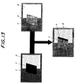
- the two image signals are synthesized by combining or exchanging them in a mosaic fashion. That is to say, as shown in Fig. 13, when a too bright portion B (e.g. background) in a first image A picked-up with a large exposure amount is replaced by a corresponding portion D in a second image C picked-up with a small exposure amount after adjusting a gain of said portion D to derive a synthesized image E, if a subject F moves from right to left in Fig. 13 during a time interval between successive image picking-up operations, a part of the subject F in the second image C picked-up with small exposure amount corresponding to the movement is also synthesized as a part G in the synthesized image E. Then, the subject is partially seen double, and therefore a feeling of strangeness remains.
- a too bright portion B e.g. background
- a synthetic unsuitable portion is detected on the basis of a comparison of a plurality of image signals picked-up with different exposure amounts, and the pixel signal of the thus detected synthetic unsuitable portion is corrected. Therefore, even if a subject moves on a bright background during successive image picking-up operations, it is possible to minimize any undesired synthesis due to the movement of the subject, and thus a corrected synthesized image having a wide dynamic range can be obtained without causing a feeling of strangeness upon comparing with the conventional photographic film.
- said synthetic unsuitable portion detecting means is constructed such that a ratio in level between a plurality of image signals picked-up with different exposure amounts is calculated, and a synthetic unsuitable portion is detected on the basis of a comparison of said ratio with a ratio in exposure amounts with which said plurality of image signals are picked-up.
- a synthetic unsuitable portion can be detected by a simple comparing operation using the plurality of image signals picked-up with different exposure amounts and data from a hardware controlling an exposing operation. Therefore, a cost can be reduced and an operation time can be shortened.
- said synthetic unsuitable portion detecting means is constructed such that a difference between a plurality of image signals picked-up with different exposure amounts is calculated, and a synthetic unsuitable portion is detected on the basis of said difference. Also in this case, a synthetic unsuitable portion can be detected by a simple comparing operation using the plurality of image signals taken with different exposure amounts and data from a hardware controlling an exposing operation, and therefore a cost can be reduced and an operation time can be shortened.
- said synthetic unsuitable portion detecting means is constructed such that a motional vector is calculated on the basis of a comparison of the plurality of image signals picked-up with different exposure amounts, and a synthetic unsuitable portion is detected on the basis of a magnitude of said motional vector.
- a moving amount and a moving direction of a subject can be derived, it is possible to detect the synthetic unsuitable portion much more precisely.
- said synthetic unsuitable portion detecting means is constructed such that a difference between said plurality of image signals picked-up with different exposure amounts is calculated, a motional vector is derived on the basis of a comparison between said plurality of image signals only for a pixel region in which an absolute value of said difference is not less than a predetermined value, and a synthetic unsuitable portion is detected on the basis of a magnitude of said motional vector.
- the operation time of detecting a synthetic unsuitable portion can be materially shortened.
- said synthetic unsuitable portion correcting means is constructed such that a pixel signal within a synthetic unsuitable portion is corrected in accordance with a synthesized pixel signal of a portion which situates in a portion which is not detected as the synthetic unsuitable portion, but is in a vicinity of the synthetic unsuitable portion.
- the pixel signal within the synthetic unsuitable portion is corrected in accordance with the synthesized pixel signal of a portion which situates near the synthetic unsuitable portion, it is possible to obtain a corrected synthesized image signal which does not produce a feeling of strangeness with respect to surroundings of the subject as well as a whole synthesized image signal.
- said synthetic unsuitable portion detecting means is constructed to detect a synthetic unsuitable portion on the basis of the motional vector
- said synthetic unsuitable portion correcting means is constructed such that a pixel signal in the synthetic unsuitable portion including a start point of the motional vector is corrected by a synthesized pixel signal in a portion including an end point of said motional vector and being excluded from said synthetic unsuitable portion, and a pixel signal of the synthetic unsuitable portion in a remaining region within the pixel block including the end point of the motional vector is corrected in accordance with an image signal of a corresponding region of one of said plurality of image signals.
- the pixel signal in the synthetic unsuitable portion including the start point of the motional vector is corrected by the synthesized pixel signal in the pixel block including the end point of said motional vector and being excluded from said synthetic unsuitable portion
- the pixel signal in the synthetic unsuitable portion including the start point of the motional vector can be corrected using a lot of pixels without the synthetic suitable portion. Therefore, the precision of the correction can be improved, and it is possible to attain a corrected synthesized image which does not cause a feeling of strangeness with respect to a whole image.
- said synthetic unsuitable portion detecting means is constructed such that a synthetic unsuitable portion is detected by calculating a motional vector
- said synthetic unsuitable portion correcting means is constructed such that a pixel signal of the synthetic unsuitable portion within a pixel block which has a center at a start point of said motional vector and contains an end point of said motional vector is corrected in accordance with a synthesized image signal of a synthetic suitable portion within a pixel block which has a center at the end point of said motional vector and has a same size as said pixel block having a center at the start point of the motional vector.
- a computer readable record medium having a program recorded thereon, wherein said program is to make a computer execute the following procedures for controlling an operation of an image pick-up device having a solid state image sensing element:
- Fig. 1 is a block diagram showing a principal structure of the image pick-up device embodying the present invention which is constructed as an electronic still camera.
- the electronic still camera comprises a single plate type color CCD image sensing element 1 having an electronic shutter function.
- On to the CCD image sensing element 1 is projected an image of an object by means of a lens unit 2 and a stop-shutter mechanism 3.
- the object image is then photoelectrically converted into an image signal.
- the image signal is amplified by an amplifier 4 and is converted into a digital signal by an A/D converter 5. Then, the thus obtained digital image data is supplied to a camera signal processing circuit 6 and is processed thereby.
- the output signal of the A/D converter 5 is also supplied to an AF, AE, AWB detection circuit 7, in which an AF detection processing for deriving AF information for automatically controlling a focus condition, an AE processing for deriving AE information for automatically controlling an exposure, and an AWB processing for deriving AWB information for automatically controlling a white balance.
- the AF information, AE information and AWB information are supplied to the lens unit 2, stop-shutter mechanism 3 and camera signal processing circuit 6, respectively through CPU 8.
- the camera signal processing circuit 6 and CPU 8 are connected to a bus line 9, to which are also connected a DRAM 11 through a memory controller 10, said DRAM being used as a working memory upon processing color of the image data, and an image compressing circuit (JPEG) 12 for compressing the image data supplied from the camera signal processing circuit 6.
- a memory card I/F 14 for storing a compressed image signal data into a memory card 13, a liquid crystal display (LCD) 16 via a display circuit 15, and a PC I/F 18 for transferring the image data stored in the memory card 13 to a personal computer (PC) 17.
- Said LCD 16 displays an image stored in the memory card 13 and various image picking-up conditions.
- a strobe flash 19 which is controlled in accordance with the AE information supplied from the AF, AE and AWB detection circuit 7, and an input key 20 for setting various image pick-up modes and driving a trigger switch.
- the CCD image sensing element 1 is driven by a timing pulse from a timing generator (TG) 21 under the control of the CPU 8.
- any one of a normal pick-up mode without image synthesis and a wide dynamic range pick-up mode with image synthesis can be selected manually or can be automatically selected by detecting a too bright portion (white large area) in an image signal from the CCD image sensing element 1 under the control of the CPU 8.
- the normal pick-up mode an image signal corresponding to a single picture is derived from the CCD image sensing element 1 by a single picking-up operation.
- the wide dynamic mode is selected, the object image is repeatedly picked-up by the CCD element 1 with different exposure amounts to derive a plurality of image signals corresponding to a plurality of pictures by a single picking-up operation.
- the CCD image sensing element 1 produces successively two image signals with different exposure amounts by a single image picking-up operation.
- the thus obtained single image signal or plural image signals are processed by the camera signal processing circuit 6 in accordance with the selected pick-up mode.
- Fig. 2 is a block diagram illustrating an embodiment of the camera signal processing circuit 6 shown in Fig. 1.
- the camera signal processing circuit 6 comprises an input side exchange switch 25 and an output side exchange switch 26.
- One contact of the input side exchange switch 25 is connected to one contact of the output side exchange switch 26 by means of a camera signal image processing circuit 27.
- the other contact of the input side exchange switch 25 is connected to a switching arm of an image exchange switch 28, whose one contact is connected to one input of an image synthesis processing circuit 32 via image buffer 29, on-off switch 30 and process circuit 31.
- the other contact of the image exchange switch 28 is connected to the other input of the image synthesis processing circuit 32 through image buffer 33, on-off switch 34 and process circuit 35.
- An output of the image synthesis processing circuit 32 is connected to an input of an image compression processing circuit 36, whose output is connected to the other input of the output side exchange switch 26.
- the input and output side exchange switches 25 and 26 are controlled by a pick-up mode signal ii from the CPU 8, and the image exchange switch 28 and on-off switches 30 and 34 are controlled by an image synthesis process control signal jj from the CPU 8 via a switching control circuit 37.
- the CPU 8 supplies, to the image synthesis processing circuit 32, a data signal representing a ratio of exposure amounts with which the object is pick-up successively.
- the input and output side exchange switches 25 and 26 are set to the position of the camera signal image processing circuit 27 by the pick-up mode signal ii. Then, the image signal aa from the A/D converter 5 is supplied to the camera signal image processing circuit 27 by means of the input side exchange switch 25, and is subjected to conventional image processes such as AWB process in accordance with the AWB information from the CPU 8, interpolating process for color information on the basis of a color filter structure of the CCD image sensing element 1, and contrast enhancing process. Then, an image signal hh thus processed is supplied to the bus line 9 as a final image signal kk through the output side exchange switch 26.
- AWB process in accordance with the AWB information from the CPU 8
- the input side exchange switch 25 is connected to the image exchange switch 28 and at the same time, the output side exchange switch 26 is connected to the image compression processing circuit 36 under the control of the pick-up mode signal ii from the CPU 8.
- the image exchange switch 28 and on-off switches 30, 34 are controlled by the image synthesis process control signal jj supplied from the CPU 8 via the switching control circuit 37, such that two image signals picked-up with different exposure amounts are successively stored in the image data buffers 29 and 33, respectively.
- the on-off switches 30 and 34 are set to the open-state, and the image exchange switch 28 is driven in synchronism with the image picking-up operations for driving the two image signals picked-up with different exposure amounts, such that the image signal aa picked-up with a smaller exposure amount is stored in the image data buffer 29 and the image signal aa picked-up with a larger exposure amount is stored in the image data buffer 33.
- the on-off switches 30, 34 are simultaneously driven into the closed-condition, an image signal bb picked-up with a smaller exposure amount is supplied from the image data buffer 29 to the process circuit 31 through the on-off switch 30 and an image signal cc picked-up with a larger exposure amount is supplied from the image data buffer 33 to the process circuit 35 through the on-off switch 34.
- the image signals are subjected to similar image processes to those of the camera signal image processing circuit 27.
- An image signal dd picked-up with a smaller exposure amount and an image signal ee picked-up with a larger exposure amount are supplied to the image synthesis processing circuit 32 in synchronism with each other.
- the image synthesis processing circuit 32 compose the image signals dd and ee by partially exchanging these image signals in accordance with the exposure amount ratio signal mm from the CPU 8 to derive a synthesized image signal ff having a wider dynamic range than the image signals dd and ee.
- the thus obtained synthesized image signal ff is supplied to the image compression processing circuit 36, in which the synthesized image signal ff is compressed such that the dynamic range is matched with a proper exposure level to derive a compressed synthesized image signal gg.
- This compressed synthesized image signal gg is supplied to the bus line 9 by means of the output side exchange switch 26 as a final output image signal kk.
- the image data buffer 33 and on-off switch 34 may be dispensed with.
- the on-off switch 30 is closed in synchronism with the switching operation of the image exchange switch 28 such that the image signal bb picked-up with a smaller exposure amount from the image data buffer 29 and the image signal aa picked-up with a larger exposure amount from the A/D converter 5 may be supplied to the process circuits 31 and 35, respectively in a synchronous manner.
- a ratio of level between these image signals is calculated pixel by pixel, and when the calculated level ratio is equal to or larger than the exposure amount ratio data signal mm from the CPU 8 by a predetermined value, a relevant pixel is judged to be a synthetic unsuitable pixel, and this pixel is corrected by performing interpolation with the synthesized image signal of a pixel which is in a vicinity of the relevant synthetic unsuitable pixel, but is not detected as a synthetic unsuitable pixel.
- Fig. 3 is a block diagram depicting an embodiment of the image synthesis processing circuit 32 of the first embodiment.
- the image signal ee picked-up with a larger exposure amount is supplied to one input of an image synthesizing unit 41 as well as to one input of an image data comparing unit 42.
- the image signal dd picked-up with a smaller exposure amount is supplied to the other input of the image data comparing unit 42 as well as to a multiplier 43.
- a gain of the image signal dd is adjusted by an amount corresponding to the exposure amount ratio on the basis of the exposure amount ratio data signal mm from the CPU 8. Then the thus adjusted image signal pp picked-up a smaller exposure amount is supplied to the other input of the image synthesizing unit 41.
- the image data comparing unit 42 the level ratio of the image signals dd and ee are compared with each other pixel by pixel to derive an image data comparison signal nn.
- the thus derived signal nn is supplied to a comparison calculating unit 44.
- the image data comparison signal nn is compared with a reference value defined by the exposure ratio data signal mm from the CPU 8 to derive a comparison result logic data signal oo, which is supplied to the image synthesizing unit 41 and an synthetic unsuitable pixel region extracting unit 45.
- the comparison result logic data signal oo is a logic "1", when the image data comparison signal nn of a pixel is larger than the reference value and the relevant pixel is judged to be the synthetic unsuitable pixel.
- the comparison result logic data signal oo is a logic "0".
- the image synthesizing unit 41 when the comparison result data logic signal oo of a pixel is "0", i.e. the relevant pixel belongs to the synthetic suitable pixel, the gain adjusted image signal pp picked-up with a smaller exposure amount and the image signal ee picked-up with a larger exposure amount are synthesized as explained above with reference to Fig. 13.
- the comparison result data logic signal oo of a relevant pixel is "1", i.e. the relevant pixel is judged to be the synthetic unsuitable pixel, the relevant pixel is not used in the image synthesis.
- the image synthesizing unit 41 supplies a synthesized image signal qq in which synthetic unsuitable pixels are not synthesized.
- the thus obtained synthesized image signal qq is supplied to an interpolation pixel detecting unit 46 and a low pass filter (LPF) 47.
- LPF low pass filter
- a synthetic unsuitable pixel region is extracted for respective lines (horizontal direction) on the basis of the logic value of the comparison result logic data signal oo, i.e. a region in which logic "1" continues, to derive a region signal rr, which is supplied to the interpolation pixel detecting unit 46 and synthetic unsuitable pixel interpolating unit 48.
- an interpolation pixel (correction reference pixel) for interpolating a pixel signal of the synthetic unsuitable pixel region in accordance with the synthesized image signal qq from the image synthesizing unit 41 and the region signal rr from the synthetic unsuitable pixel region extracting unit 45 to derive a correction reference pixel signal ss (including the information of the synthesized image signal qq).
- the thus derived correction reference pixel signal ss is supplied to a synthetic unsuitable pixel interpolating unit 48.
- a pixel signal of the synthetic unsuitable pixels corresponding to the region signal rr from the synthetic unsuitable pixel region extracting unit 45 is corrected by the interpolation on the basis of the correction reference pixel signal ss from the interpolation pixel detecting unit 46 to derive an interpolated synthesized correct pixel signal tt, which is then supplied to the low pass filter 47.
- the synthesized correct pixel signal tt is subjected to the low pass filtering treatment at least in the vertical direction by means of the synthesized image signal qq from the image synthesizing unit 41 to derive a synthesized image signal which is supplied to the image compression processing circuit 36 shown in Fig. 2 as the synthesized image signal ff.
- Fig. 4 is a flow chart representing the correcting operation for the synthetic unsuitable pixel by means of the synthetic unsuitable pixel region extracting unit 45, interpolation pixel detecting unit 46, synthetic unsuitable pixel interpolating unit 48 and low pass filter 47 shown in Fig. 3.
- the synthetic unsuitable pixel region extracting unit 45 judges whether or not a reference pixel belongs to the comparison unsuitable pixel on the basis of the comparison result logic data signal oo from the comparison calculating unit 44 (step S1).
- the synthetic unsuitable pixel region extracting unit 45 judges whether or not a reference pixel belongs to the comparison unsuitable pixel on the basis of the comparison result logic data signal oo from the comparison calculating unit 44 (step S1).
- the synthetic unsuitable pixel region extracting unit 45 judges whether or not a reference pixel belongs to the comparison unsuitable pixel on the basis of the comparison result logic data signal oo from the comparison calculating unit 44 (step S1).
- the pixel is judged as the synthetic unsuitable one,
- a plurality of synthetic unsuitable pixels aligned in the horizontal direction are unified into a single region (step S2), and a length (S) of this synthetic unsuitable pixel region (step S3).
- the synthetic unsuitable pixels defined by this length constitutes the region signal rr.
- pixels situating at positions which are separated from respective ends of the synthetic unsuitable pixel region by a distance S ⁇ are detected as correction reference pixels (LPx, RPx) in a step S4.
- luminance signals (Y-LPx, Y-RPx) of the thus detected correction reference pixels are calculated in a step S5, and the thus calculated luminance signals are compared with each other in a step S6.
- Y-LPx Y-RPx
- color difference signals (Cr-LPx, Cr-RPx) are calculated in a step S7.
- the pixel signal within the correction region is interpolated in accordance with the correction reference pixel signal by smoothing the pixel signal for respective luminance signal and color difference signal (step S10).
- the luminance and color difference signals of the correction region are subjected to the low pass filtering treatment (step S11).
- the interpolated luminance and color difference signals are converted into RGB signals (step S12), and the thus converted signals are supplied as the synthesized image signal ff.
- the synthetic unsuitable pixel region is calculated and corrected only in the horizontal direction.
- the synthetic unsuitable pixel region may be also calculated in the vertical direction, and the pixel signal of this region may be corrected in both the horizontal and vertical directions in accordance with the correction reference pixel signal.
- the low pass filtering treatment may be conducted in a two-dimensional manner in the horizontal and vertical directions. In this case, it is possible to obtain the synthesized image from which a feeling of strangeness is removed much more effectively with respect to the surroundings and whole synthesized image.
- the synthetic unsuitable region is corrected pixel by pixel, but according to the invention, the synthetic unsuitable region may be detected and corrected for a block including a given number of pixels.
- a vector representing a movement of a subject (here this vector is called motional vector) is calculated by comparing these image signals.
- motional vector When the motional vector of pixels exceeds a predetermined value, the relevant pixels are detected as the synthetic unsuitable pixel.
- a pixel signal at a start point of the motional vector is corrected by performing the interpolation in accordance with a synthesized image signal of a synthetic suitable part within a small block including an end point of the motional vector, and a pixel signal of the remaining synthetic unsuitable region within the small block including the end point of the motional vector is corrected by conducting the interpolation in accordance with a pixel signal of a corresponding region of the image signal dd.
- Fig. 5 is a block diagram showing an embodiment of the image synthesis processing circuit 32 in the second embodiment of the image pick-up device according to the invention.
- the image signal ee picked-up with a larger exposure amount is supplied to one input of an image synthesizing unit 51.
- the image signal dd picked-up with a smaller exposure amount is supplied to a multiplier 52, in which a gain of the image signal is adjusted on the basis of the exposure amount ratio data signal mm from the CPU 8 by an amount corresponding to the exposure amount ratio.
- the amplified image signal pp is supplied to the other input of the image synthesizing unit 51.
- the image signals pp and ee are supplied to edge detecting units 53 and 54, respectively to derive edge detection signals uu and vv. These edge detection signals are supplied to block setting units 55 and 56, respectively to derive block signals ww and xx, which are supplied to a motional vector calculating unit 57.
- a motional vector representing the movement of the subject is calculated in accordance with the block signals ww and xx to derive a motional vector data signal yy.
- the thus derived motional vector data signal yy is supplied to the image synthesizing unit 51, small block setting unit 58, small block average calculating unit 59 and vector pixel interpolating unit 60.
- the motional vector data signal yy is compared with a predetermined threshold value.
- a relevant pixel is judged as a synthetic suitable pixel and a pixel signal of the gain adjusted image signal pp picked-up with a smaller exposure amount and a corresponding pixel signal of the image signal ee picked-up with a larger exposure amount are synthesized by the partial exchanging in the manner explained with reference to Fig. 13.
- a pixel is judged as a synthetic unsuitable pixel and the image synthesis by the partial exchange is not executed.
- the image synthesizing unit 51 produce the synthesized image signal qq in which pixels except for the synthetic unsuitable pixels are synthesized.
- the thus derived image synthesized signal qq is supplied to the small block setting unit 58 and low pass filter (LPF) 61.
- LPF low pass filter
- a magnitude of the motional vector data signal yy having a start point of a relevant pixel is compared with a predetermined threshold value. Only when the motional vector data signal yy exceeds the threshold value, the relevant pixel is judged as a synthetic unsuitable pixel. Then, as illustrated by (A) in Fig. 6, a small block (here 3 ⁇ 3 pixel block) is set from the synthesized image signal qq such that a center of the block corresponds to the end point of the motional vector to derive a small block set signal zz.
- This signal zz (including the information of the synthesized image signal qq) is then supplied to the small block average calculating unit 59, in which average values (Rv, Gv, Bv) of respective color signals by using the synthesized image signal within the small block as shown by (B) in Fig. 6. Then, a small block average value signal aaa (including the information of the synthesized image signal qq) is supplied to the vector pixel interpolating unit 60.
- To the vector pixel interpolating unit 60 is also supplied the gain adjusted image signal pp picked-up with a smaller exposure amount, and as depicted by (C) in Fig. 6, in order to remove a moving object into an original position, a pixel signal of the synthetic unsuitable pixel at the start point of the motional vector is interpolated by the small block average signal aaa.
- the pixel signal of the synthetic unsuitable region including the end point of the motional vector is interpolated by the pixel signal of a corresponding region of the gain adjusted image signal pp.
- a synthesized corrected image signal bbb is supplied to the low pass filter 61.
- the synthesized corrected image signal bbb is subjected to the low pass filtering treatment by using the synthesized image signal qq from the image synthesizing unit 51 like as the first embodiment to derive the synthesized image signal ff.
- Fig. 7 is a flow chart representing the interpolating operation for a pixel signal of synthetic unsuitable pixels by means of the small block setting unit 58, small block average calculating unit 59, vector pixel interpolating unit 60 and low pass filter 61 shown in Fig. 5.
- the small block setting unit 58 it is judged whether or not the motional vector having a start point corresponding to a relevant pixel exceeds the predetermined threshold value (step S21).
- the relevant pixel is judged to be a synthetic unsuitable pixel, and a small block having a size of 3 ⁇ 3 pixels such that said small has a center corresponding to an end point of the motional vector in accordance with the synthesized image signal qq from the image synthesizing unit 51 (step S22). Then, the small block set signal zz is supplied to the small block average calculating unit 59.
- step S23 variables (R B , G B , B B ) of color signals and a count value (Count) of an inside counter counting the number of adding operations are initialized (step S23), and while the small block is scanned (step S24), it is judged whether or not the synthesized pixel signals (R, G, B) are existent within the small block (step S25). When the synthesized pixel signals are existent, the relevant synthesized pixel signals are added to corresponding variables and the count values are incremented by one (step S26).
- step S27 After completing the scanning for all the small block (step S27), averages (R V , G V , B V ) of the variables (R B , G B , B B ) are calculated by using the count values (Count) (step S28), and the thus calculated average values are supplied to the vector pixel interpolating unit 60 as the small block average signal aaa.
- a pixel signal of a synthetic unsuitable pixel at the start point of the motional vector is interpolated by the small block average signal aaa (step S29), and a pixel signal of the remaining synthetic unsuitable pixel region including the end point of the motional vector is interpolated by a pixel signal of a corresponding region of the gain adjusted image signal pp (step S30).
- the thus obtained pixel signal is supplied to the low pass filter 61 as the synthesized corrected image signal bbb.
- the pixel signal on the motional vector interpolated in accordance with the synthesized image signal qq is subjected to the low pass filtering treatment (step S31) to derive the synthesized image signal ff.
- the motional vector is detected from the gain adjusted image signal picked-up with a shorter exposure time and the image signal picked-up with a longer exposure time, and these image signals are synthesized in a partially exchanging manner except for a region in which the detected motional vector exceeds the predetermined threshold value to obtain the synthesized image signal as depicted by (D) in Fig. 8. It should be noted that at this time, the start point of the motional vector shown by (D) in Fig. 8 has not been replaced yet.
- a pixel signal of a pixel corresponding to a start point of a motional vector is interpolated by an average value of the synthesized image signals within a small block having a center corresponding to an end point of the motional vector as explained above with reference to Fig. 6.
- the start point of the motional vector is replaced by the average value of the synthesized image signals within the small block as shown by (D) in Fig. 8 .
- the pixel signal of the remaining region containing the end point of the motional vector is interpolated by the pixel signal of a corresponding region of the gain adjusted image signal illustrated by a white frame in (C) in Fig. 8.
- the pixel signal at a boundary between before and after the movement of the picked-up object is corrected (interpolated)
- a background may be equally corrected (interpolated).
- an average value of synthesized image signals within a small block set at an end point of a motional vector is calculated, and a pixel signal at a start point of the motional vector is interpolated in accordance with said average value.
- the information of a moving object is dominant in the average value.
- a pixel signal except for the start point of the motional vector is interpolated by a pixel signal of a corresponding region of the image signal picked-up with a shorter exposure time (corresponding to a smaller exposure amount).
- the pixel signal at the start point of the motional vector is interpolated by the average value of the image signals within a small block having a center corresponding to the end point of the motional vector. According to an embodiment of the invention, it is also possible to replace the pixel signal at the start point of the motional vector merely by the pixel signal at the end point of the motional vector.
- a difference between these image signals is calculated, and for a pixel region in which an absolute value of said difference exceeds a predetermined threshold value, a motional vector is calculated.
- a relevant pixel is judged to be a synthetic unsuitable pixel.
- a pixel block having a center corresponding to a start point of the motional vector and including an end point of the motional vector is set, relevant synthetic unsuitable pixel, and a pixel signal of a synthetic unsuitable region within the pixel block is replaced by a synthesized image signal of a synthetic suitable region within a pixel block having a center corresponding to the end point of the motional vector and a size identical with said pixel block having a center at the start point of the motional vector.
- a pixel signal which is lost by the replacement is corrected by a pixel signal of a corresponding region of the gain adjusted image signal picked-up with a small exposure amount.
- Fig. 11 is a block diagram showing an embodiment of the image synthesis processing circuit 32 of the third embodiment.
- the image signal ee picked-up with a larger exposure amount is supplied to one input of an image synthesizing unit 70, and the image signal dd picked-up with a smaller exposure amount is supplied to a multiplier 71, in which a gain of the image signal is amplified by the exposure amount ratio in accordance with the exposure amount ratio data signal mm from the CPU 8.
- the gain adjusted image signal pp is supplied to the other input of the image synthesizing unit 70.
- the image signals pp and ee are supplied to AND gates 72 and 73, respectively as well as to an image difference calculating unit 74.
- differences between the image signals pp and ee are calculated on a pixel by pixel basis, i.e. at corresponding pixel positions, and absolute values of the differences are compared with a predetermined threshold value.
- a logic "1” is derived, and when an absolute value of a difference is not larger than the threshold value, a logic "0" is produced as a comparison result logic data signal ccc.
- This comparison result logic data signal ccc is supplied to the other inputs of the AND gates 72 and 73.
- the AND gate 72 generates an image signal ddd of a region in which the absolute value of the difference between the image signals pp and ee exceeds the threshold value among the gain adjusted image signal pp
- the AND gate 73 generates an image signal eee of a region in which the absolute value of the difference between the image signals pp and ee exceeds the threshold value among the image signal ee.
- the image signals ddd and eee generated from the AND gates 72 and 73 are supplied to edge detecting units 75 and 76, respectively and edge detection signals fff and ggg are supplied to block setting units 77 and 78, respectively to produce block signals ww and xx.
- These block signals ww and xx are supplied to a motional vector calculating unit 79, in which a motional vector is calculated on the basis of the block signals ww and xx to derive a motional vector data signal yy.
- the thus obtained motional vector data signal yy is supplied to the image synthesizing unit 70, corrected block setting unit 80, corrected block replacement pixel determining unit 81 and data correcting unit 82.
- the motional vector data signal yy is compared with a predetermined threshold value, and the motional vector data signal yy is not larger than the threshold value, a relevant pixel is judged to be a synthetic suitable pixel. Then, corresponding pixels of the gain adjusted image signal pp picked-up with a smaller exposure amount and the image signal ee picked-up with a larger exposure amount are combined by performing the exchange in a mosaic manner explained with reference to Fig. 13. When the motional vector data signal yy exceeds the predetermined threshold value, a relevant pixel is judged as a synthetic unsuitable pixel, and the image synthesis by the exchange is not carried out.
- the image synthesizing unit 70 derives the synthesized image signal qq, in which pixels other than synthetic unsuitable pixels are synthesized in a mosaic manner, and this synthesized image signal qq is supplied to the corrected block setting unit 80 and low pass filter (LPF) 83.
- LPF low pass filter
- a motional vector data signal yy having a start point corresponding to a pixel under consideration is compared with a predetermined threshold value Th (step S41). Only when the motional vector data signal yy exceeds the threshold value Th, the relevant pixel is judged as a synthetic unsuitable pixel, and a corrected block is set by a similar calculation for deriving the motional vector such that said block has a center corresponding to a start point of the motional vector and includes an end point of the motional vector (step S42).
- a corrected block set signal hhh (including the information of the synthesized image signal qq) is supplied to the corrected block replacement pixel determining unit 81.
- a correction block having the same size as the corrected block and having a center corresponding to the end point of the motional vector in accordance with the corrected block set signal hhh and motional vector data signal yy (step S43).
- a correction block set signal iii (including the information of the synthesized image signal qq) is supplied to the data correcting unit 82.
- a pixel signal of a synthetic unsuitable pixel is replaced by the synthesized image signal within the correction block in accordance with the correction block set signal iii and motional vector data signal yy (step S44).
- a pixel signal of the relevant region which has been lost by the replacement is obtained by performing the interpolation in accordance with a pixel signal of a corresponding region of the gain adjusted image signal pp picked-up with a smaller exposure amount (step S45). In this manner, a synthesized corrected image signal jjj is obtained and is supplied to the low pass filter 83.
- the pixel signal within the corrected block as well as the pixel signal in a region surrounding the corrected block are subjected to the low pass filtering treatment for respective color signals (step S46) to derive the synthesized image signal ff.
- the pixel signal of the synthetic unsuitable region within the corrected block is replaced by the synthesized image signal of the synthetic suitable region within the correcting block, but according to an embodiment of the invention, the interpolation may be utilized instead of the replacement or substitution. Then, no pixel signal is lost within the correcting block and it is no more necessary to perform the above mentioned interpolation for the lost pixel signal. In this manner, the process can be simplified.
- An aspect of the present invention also provides a computer readable record medium, having a program recorded thereon, wherein said program is to make a computer execute the procedure for controlling an operation of the image pick-up device in the dynamic range image picking-up mode in the manner explained above in the various embodiments and possible alternations thereof.
- a synthetic unsuitable region in the image signals is detected and a pixel signal of such a synthetic unsuitable region is corrected. Therefore, the influence of the movement of a subject on a bright background during successive picking-up operations upon the synthesizing of the image signals can be minimized, and it is possible to obtain an image having a wide dynamic range which does not cause any feeling of strangeness as compared with a conventional photographic image.
Landscapes
- Engineering & Computer Science (AREA)
- Multimedia (AREA)
- Signal Processing (AREA)
- Computing Systems (AREA)
- Theoretical Computer Science (AREA)
- Transforming Light Signals Into Electric Signals (AREA)
- Studio Devices (AREA)
Applications Claiming Priority (2)
| Application Number | Priority Date | Filing Date | Title |
|---|---|---|---|
| JP20945098 | 1998-07-24 | ||
| JP20945098A JP4282113B2 (ja) | 1998-07-24 | 1998-07-24 | 撮像装置および撮像方法、並びに、撮像プログラムを記録した記録媒体 |
Publications (1)
| Publication Number | Publication Date |
|---|---|
| EP0975154A1 true EP0975154A1 (en) | 2000-01-26 |
Family
ID=16573080
Family Applications (1)
| Application Number | Title | Priority Date | Filing Date |
|---|---|---|---|
| EP99305841A Withdrawn EP0975154A1 (en) | 1998-07-24 | 1999-07-23 | Image pick-up device |
Country Status (3)
| Country | Link |
|---|---|
| US (3) | US6801248B1 (enExample) |
| EP (1) | EP0975154A1 (enExample) |
| JP (1) | JP4282113B2 (enExample) |
Cited By (3)
| Publication number | Priority date | Publication date | Assignee | Title |
|---|---|---|---|---|
| WO2003083773A3 (en) * | 2002-03-27 | 2004-03-11 | Univ Columbia | Imaging method and system |
| DE102006046720A1 (de) * | 2006-10-02 | 2008-04-03 | Arnold & Richter Cine Technik Gmbh & Co. Betriebs Kg | Digitale Laufbildkamera |
| CN102387291A (zh) * | 2010-08-31 | 2012-03-21 | 索尼公司 | 成像设备、信号处理方法和程序 |
Families Citing this family (57)
| Publication number | Priority date | Publication date | Assignee | Title |
|---|---|---|---|---|
| JP4282113B2 (ja) * | 1998-07-24 | 2009-06-17 | オリンパス株式会社 | 撮像装置および撮像方法、並びに、撮像プログラムを記録した記録媒体 |
| US7428011B1 (en) * | 1999-09-02 | 2008-09-23 | Fujifilm Corporation | Wide dynamic range electronic image recording and reproducing system |
| EP1237363B1 (en) * | 1999-11-22 | 2006-01-18 | Matsushita Electric Industrial Co., Ltd. | Solid-state imaging device |
| US7050094B2 (en) * | 2000-10-26 | 2006-05-23 | Micron Technology, Inc. | Wide dynamic range operation for CMOS sensor with freeze-frame shutter |
| JP2002218328A (ja) * | 2001-01-19 | 2002-08-02 | Ricoh Co Ltd | 画像入力装置、画像入力方法、およびその方法を実行するためのプログラムを格納したことを特徴とするコンピュータが読み取り可能な記録媒体 |
| JP4511066B2 (ja) * | 2001-03-12 | 2010-07-28 | オリンパス株式会社 | 撮像装置 |
| JP4028694B2 (ja) * | 2001-04-27 | 2007-12-26 | 松下電器産業株式会社 | カメラ装置および当該カメラ装置を具備する電子装置 |
| JP3624859B2 (ja) * | 2001-06-19 | 2005-03-02 | カシオ計算機株式会社 | 撮像装置、ソフトフォーカス画像撮影方法 |
| JP4742453B2 (ja) * | 2001-06-20 | 2011-08-10 | ソニー株式会社 | 撮像方法および装置 |
| US7262794B2 (en) | 2001-08-20 | 2007-08-28 | Photographic Art Research Laboratory | Method of making digital photograph and digital photograph made by that method |
| JP4154157B2 (ja) * | 2002-02-25 | 2008-09-24 | 株式会社東芝 | 撮像装置 |
| US7508421B2 (en) * | 2002-06-24 | 2009-03-24 | Fujifilm Corporation | Image pickup apparatus and image processing method |
| JP4025207B2 (ja) * | 2003-01-17 | 2007-12-19 | 富士フイルム株式会社 | 固体撮像素子及びデジタルカメラ |
| US7889275B2 (en) * | 2003-01-28 | 2011-02-15 | Microsoft Corp. | System and method for continuous flash |
| WO2004114677A1 (ja) | 2003-06-23 | 2004-12-29 | Sony Corporation | 画像処理方法および装置、並びにプログラム |
| JP4392583B2 (ja) * | 2003-06-27 | 2010-01-06 | ソニー株式会社 | 信号処理装置および信号処理方法、並びにプログラムおよび記録媒体 |
| FI20045445A0 (fi) * | 2004-11-18 | 2004-11-18 | Nokia Corp | Menetelmä, laitteisto, ohjelmisto ja järjestely kuvadatan muokkaamiseksi |
| US7616231B2 (en) * | 2005-01-06 | 2009-11-10 | Goodrich Corporation | CMOS active pixel sensor with improved dynamic range and method of operation for object motion detection |
| JP4731953B2 (ja) * | 2005-03-02 | 2011-07-27 | 富士フイルム株式会社 | 撮像装置、撮像方法、及び撮像プログラム |
| JP4687265B2 (ja) * | 2005-06-14 | 2011-05-25 | 富士ゼロックス株式会社 | 画像分析装置 |
| JP2007124609A (ja) * | 2005-09-28 | 2007-05-17 | Nissan Motor Co Ltd | 車両周囲映像提供装置 |
| JP4509925B2 (ja) * | 2005-12-27 | 2010-07-21 | 株式会社メガチップス | 画像処理装置及びカメラシステム並びに画像処理方法及び動画像表示方法 |
| WO2007077719A1 (ja) * | 2005-12-27 | 2007-07-12 | Kyocera Corporation | 撮像装置およびその画像処理方法 |
| JP2007300463A (ja) * | 2006-05-01 | 2007-11-15 | Opt Kk | カメラ装置および画像処理方法 |
| JP5011814B2 (ja) * | 2006-05-15 | 2012-08-29 | ソニー株式会社 | 撮像装置、および画像処理方法、並びにコンピュータ・プログラム |
| TW200820123A (en) * | 2006-10-20 | 2008-05-01 | Primax Electronics Ltd | Method and system of generating high dynamic range image corresponding to specific scene |
| JP4806329B2 (ja) * | 2006-10-23 | 2011-11-02 | 三洋電機株式会社 | 撮像装置及び撮像方法 |
| KR20080037965A (ko) * | 2006-10-27 | 2008-05-02 | 삼성테크윈 주식회사 | 동영상 촬영장치의 제어방법 및 이를 채용한 동영상촬영장치 |
| KR20080076004A (ko) * | 2007-02-14 | 2008-08-20 | 삼성전자주식회사 | 촬상장치 및 그 다이나믹 레인지 확장방법 |
| JP4905187B2 (ja) * | 2007-03-09 | 2012-03-28 | ソニー株式会社 | 画像処理装置、撮像装置、および画像処理方法、並びにコンピュータ・プログラム |
| JP5188101B2 (ja) | 2007-06-01 | 2013-04-24 | 株式会社キーエンス | 拡大観察装置、拡大画像撮影方法、拡大画像撮影プログラム及びコンピュータで読み取り可能な記録媒体 |
| JP4872830B2 (ja) * | 2007-06-28 | 2012-02-08 | セイコーエプソン株式会社 | 撮像装置、撮像方法、画像処理装置、画像処理プログラム及び画像処理方法 |
| US20090059039A1 (en) * | 2007-08-31 | 2009-03-05 | Micron Technology, Inc. | Method and apparatus for combining multi-exposure image data |
| JP5006835B2 (ja) * | 2008-05-07 | 2012-08-22 | ルネサスエレクトロニクス株式会社 | エラー低減方法及びエラー低減装置 |
| JP5083046B2 (ja) * | 2008-06-03 | 2012-11-28 | ソニー株式会社 | 撮像装置及び撮像方法 |
| KR101534317B1 (ko) * | 2008-10-10 | 2015-07-06 | 삼성전자주식회사 | 높은 동적 대역(hdr) 영상 생성방법 및 장치 |
| US20100091119A1 (en) | 2008-10-10 | 2010-04-15 | Lee Kang-Eui | Method and apparatus for creating high dynamic range image |
| US8666153B2 (en) * | 2008-11-04 | 2014-03-04 | Konica Minolta Opto, Inc. | Image input apparatus |
| US8073246B2 (en) | 2008-11-07 | 2011-12-06 | Omnivision Technologies, Inc. | Modifying color and panchromatic channel CFA image |
| US20100157079A1 (en) | 2008-12-19 | 2010-06-24 | Qualcomm Incorporated | System and method to selectively combine images |
| JP5214538B2 (ja) * | 2009-05-25 | 2013-06-19 | オリンパス株式会社 | 画像取得装置、画像合成方法、及び顕微鏡システム |
| KR101614914B1 (ko) * | 2009-07-23 | 2016-04-25 | 삼성전자주식회사 | 모션 적응적 고대비 영상 획득 장치 및 방법 |
| JP5458865B2 (ja) * | 2009-09-18 | 2014-04-02 | ソニー株式会社 | 画像処理装置、撮像装置、および画像処理方法、並びにプログラム |
| JP5589446B2 (ja) * | 2009-09-18 | 2014-09-17 | ソニー株式会社 | 画像処理装置、撮像装置、および画像処理方法、並びにプログラム |
| KR101604068B1 (ko) * | 2009-09-22 | 2016-03-17 | 삼성전자주식회사 | 고대비 영상 생성 장치 및 방법 |
| JP5493942B2 (ja) * | 2009-12-15 | 2014-05-14 | ソニー株式会社 | 撮像装置と撮像方法 |
| KR101643319B1 (ko) * | 2010-01-11 | 2016-07-27 | 삼성전자주식회사 | 하이 다이나믹 레인지 영상을 획득하는 장치 및 그 방법 |
| JP5772044B2 (ja) * | 2011-02-17 | 2015-09-02 | カシオ計算機株式会社 | 撮像装置、撮像方法及びプログラム |
| JP5934929B2 (ja) * | 2011-05-27 | 2016-06-15 | パナソニックIpマネジメント株式会社 | 画像処理装置および画像処理方法 |
| US8965120B2 (en) | 2012-02-02 | 2015-02-24 | Canon Kabushiki Kaisha | Image processing apparatus and method of controlling the same |
| JP6046966B2 (ja) | 2012-04-19 | 2016-12-21 | キヤノン株式会社 | 画像処理装置及び画像処理方法、プログラム、並びに記憶媒体 |
| JP6061488B2 (ja) * | 2012-04-26 | 2017-01-18 | キヤノン株式会社 | 画像処理装置及び画像処理方法 |
| JP2014039169A (ja) * | 2012-08-16 | 2014-02-27 | Sony Corp | 画像処理装置、および画像処理方法、並びにプログラム |
| JP2014050042A (ja) * | 2012-09-03 | 2014-03-17 | Toshiba Corp | 画像処理装置及び固体撮像装置 |
| JP6415037B2 (ja) * | 2013-11-12 | 2018-10-31 | キヤノン株式会社 | 撮像装置、クライアント装置、撮像装置の制御方法、クライアント装置の制御方法、及びプログラム |
| WO2015141487A1 (ja) * | 2014-03-18 | 2015-09-24 | ソニー株式会社 | 画像処理装置、画像処理方法、およびプログラム |
| TWI558204B (zh) * | 2014-11-25 | 2016-11-11 | Trans Electric Co Ltd | Image capture system |
Citations (2)
| Publication number | Priority date | Publication date | Assignee | Title |
|---|---|---|---|---|
| JPH02280585A (ja) * | 1989-04-21 | 1990-11-16 | Olympus Optical Co Ltd | 撮像装置 |
| US5309243A (en) * | 1992-06-10 | 1994-05-03 | Eastman Kodak Company | Method and apparatus for extending the dynamic range of an electronic imaging system |
Family Cites Families (18)
| Publication number | Priority date | Publication date | Assignee | Title |
|---|---|---|---|---|
| JP3467047B2 (ja) * | 1992-08-21 | 2003-11-17 | 富士写真フイルム株式会社 | 画像処理装置および方法ならびにビデオ・カメラ |
| US5764287A (en) * | 1992-08-31 | 1998-06-09 | Canon Kabushiki Kaisha | Image pickup apparatus with automatic selection of gamma correction valve |
| JP3386495B2 (ja) * | 1992-09-14 | 2003-03-17 | 富士写真フイルム株式会社 | ディジタル電子スチル・カメラおよびその制御方法 |
| US5365269A (en) * | 1992-10-22 | 1994-11-15 | Santa Barbara Instrument Group, Inc. | Electronic camera with automatic image tracking and multi-frame registration and accumulation |
| JP3074967B2 (ja) * | 1992-10-27 | 2000-08-07 | 松下電器産業株式会社 | 高ダイナミックレンジ撮像・合成方法及び高ダイナミックレンジ撮像装置 |
| US6204881B1 (en) * | 1993-10-10 | 2001-03-20 | Canon Kabushiki Kaisha | Image data processing apparatus which can combine a plurality of images at different exposures into an image with a wider dynamic range |
| US5929908A (en) * | 1995-02-03 | 1999-07-27 | Canon Kabushiki Kaisha | Image sensing apparatus which performs dynamic range expansion and image sensing method for dynamic range expansion |
| US6002433A (en) * | 1995-08-29 | 1999-12-14 | Sanyo Electric Co., Ltd. | Defective pixel detecting circuit of a solid state image pick-up device capable of detecting defective pixels with low power consumption and high precision, and image pick-up device having such detecting circuit |
| US6278490B1 (en) * | 1996-05-23 | 2001-08-21 | Olympus Optical Co., Ltd. | Exposure control for an image pickup apparatus that uses an electronic flash |
| JP3817301B2 (ja) | 1996-05-28 | 2006-09-06 | キヤノン株式会社 | 電子カメラ |
| JP3834130B2 (ja) * | 1996-07-19 | 2006-10-18 | 株式会社リコー | デジタルカメラ |
| JPH10126663A (ja) * | 1996-10-14 | 1998-05-15 | Ricoh Co Ltd | 画像入力装置及び画像入力システム |
| JP3974964B2 (ja) * | 1996-11-08 | 2007-09-12 | オリンパス株式会社 | 画像処理装置 |
| US7057653B1 (en) * | 1997-06-19 | 2006-06-06 | Minolta Co., Ltd. | Apparatus capable of image capturing |
| JPH11166279A (ja) | 1997-12-05 | 1999-06-22 | Kokuyo Co Ltd | 間仕切 |
| US6529640B1 (en) * | 1998-06-09 | 2003-03-04 | Nikon Corporation | Image processing apparatus |
| JP4282113B2 (ja) * | 1998-07-24 | 2009-06-17 | オリンパス株式会社 | 撮像装置および撮像方法、並びに、撮像プログラムを記録した記録媒体 |
| JP4511066B2 (ja) * | 2001-03-12 | 2010-07-28 | オリンパス株式会社 | 撮像装置 |
-
1998
- 1998-07-24 JP JP20945098A patent/JP4282113B2/ja not_active Expired - Fee Related
-
1999
- 1999-07-22 US US09/358,538 patent/US6801248B1/en not_active Expired - Fee Related
- 1999-07-23 EP EP99305841A patent/EP0975154A1/en not_active Withdrawn
-
2004
- 2004-04-30 US US10/835,316 patent/US7372487B2/en not_active Expired - Fee Related
-
2007
- 2007-02-23 US US11/678,400 patent/US20070139547A1/en not_active Abandoned
Patent Citations (2)
| Publication number | Priority date | Publication date | Assignee | Title |
|---|---|---|---|---|
| JPH02280585A (ja) * | 1989-04-21 | 1990-11-16 | Olympus Optical Co Ltd | 撮像装置 |
| US5309243A (en) * | 1992-06-10 | 1994-05-03 | Eastman Kodak Company | Method and apparatus for extending the dynamic range of an electronic imaging system |
Non-Patent Citations (1)
| Title |
|---|
| PATENT ABSTRACTS OF JAPAN vol. 015, no. 050 (E - 1030) 6 February 1991 (1991-02-06) * |
Cited By (6)
| Publication number | Priority date | Publication date | Assignee | Title |
|---|---|---|---|---|
| WO2003083773A3 (en) * | 2002-03-27 | 2004-03-11 | Univ Columbia | Imaging method and system |
| US7495699B2 (en) | 2002-03-27 | 2009-02-24 | The Trustees Of Columbia University In The City Of New York | Imaging method and system |
| DE102006046720A1 (de) * | 2006-10-02 | 2008-04-03 | Arnold & Richter Cine Technik Gmbh & Co. Betriebs Kg | Digitale Laufbildkamera |
| US7940316B2 (en) | 2006-10-02 | 2011-05-10 | Arnold & Richter Cine Technik Gmbh & Co. Betriebs Kg | Digital motion picture camera which combines images of different exposure times |
| CN102387291A (zh) * | 2010-08-31 | 2012-03-21 | 索尼公司 | 成像设备、信号处理方法和程序 |
| EP2424228A3 (en) * | 2010-08-31 | 2013-05-01 | Sony Corporation | Imaging apparatus, signal processing unit and method , and program |
Also Published As
| Publication number | Publication date |
|---|---|
| JP2000050173A (ja) | 2000-02-18 |
| US20040201759A1 (en) | 2004-10-14 |
| JP4282113B2 (ja) | 2009-06-17 |
| US7372487B2 (en) | 2008-05-13 |
| US20070139547A1 (en) | 2007-06-21 |
| US6801248B1 (en) | 2004-10-05 |
Similar Documents
| Publication | Publication Date | Title |
|---|---|---|
| US6801248B1 (en) | Image pick-up device and record medium having recorded thereon computer readable program for controlling the image pick-up device | |
| US7301563B1 (en) | Image pickup apparatus | |
| US7782362B2 (en) | Image pickup device for changing a resolution of frames and generating a static image based on information indicating the frames | |
| JP3630905B2 (ja) | 撮像方法及び撮像装置 | |
| KR101008917B1 (ko) | 화상 처리 방법 및 장치와 그 프로그램을 기록한 기록 매체 | |
| JP5112104B2 (ja) | 画像処理装置及び画像処理プログラム | |
| JP4567593B2 (ja) | 撮像装置および撮影方法 | |
| KR100626685B1 (ko) | 디지털 카메라 | |
| JP4987355B2 (ja) | 撮像装置および撮像方法 | |
| US11722788B2 (en) | Image processing apparatus and method, and image capturing apparatus | |
| JP2003158669A (ja) | 撮像装置 | |
| EP4002830A2 (en) | Image pick up apparatus, image pick up method, and storage medium | |
| JP4246244B2 (ja) | 撮像装置 | |
| KR101612853B1 (ko) | 촬영장치, 촬영장치의 제어방법 및 제어방법을 실행시키기 위한 프로그램을 저장한 기록매체 | |
| JP4670663B2 (ja) | 画像生成装置および画像生成プログラム | |
| JP6828069B2 (ja) | 撮像装置、撮像方法およびプログラム | |
| JP2007251997A (ja) | 撮像装置 | |
| JP3368012B2 (ja) | 画像データ処理装置 | |
| JP2021097350A (ja) | 画像処理装置、撮像装置、画像処理方法、プログラムおよび記録媒体 | |
| JP2023026997A (ja) | 撮像装置、撮像方法、プログラムおよび記録媒体 | |
| JP2001177760A (ja) | 撮像装置及び撮像方法 | |
| JP2007325129A (ja) | 撮像装置、撮像装置の制御方法、プログラム及び記憶媒体 |
Legal Events
| Date | Code | Title | Description |
|---|---|---|---|
| PUAI | Public reference made under article 153(3) epc to a published international application that has entered the european phase |
Free format text: ORIGINAL CODE: 0009012 |
|
| AK | Designated contracting states |
Kind code of ref document: A1 Designated state(s): DE |
|
| AX | Request for extension of the european patent |
Free format text: AL;LT;LV;MK;RO;SI |
|
| 17P | Request for examination filed |
Effective date: 20000419 |
|
| AKX | Designation fees paid |
Free format text: DE |
|
| 17Q | First examination report despatched |
Effective date: 20070316 |
|
| RAP1 | Party data changed (applicant data changed or rights of an application transferred) |
Owner name: OLYMPUS CORPORATION |
|
| STAA | Information on the status of an ep patent application or granted ep patent |
Free format text: STATUS: THE APPLICATION IS DEEMED TO BE WITHDRAWN |
|
| 18D | Application deemed to be withdrawn |
Effective date: 20110201 |