EP0949850B1 - Flexible substrates for electronic or optoelectronic devices - Google Patents
Flexible substrates for electronic or optoelectronic devices Download PDFInfo
- Publication number
- EP0949850B1 EP0949850B1 EP99302512A EP99302512A EP0949850B1 EP 0949850 B1 EP0949850 B1 EP 0949850B1 EP 99302512 A EP99302512 A EP 99302512A EP 99302512 A EP99302512 A EP 99302512A EP 0949850 B1 EP0949850 B1 EP 0949850B1
- Authority
- EP
- European Patent Office
- Prior art keywords
- layer
- plastic
- glass
- composite structure
- electrode
- Prior art date
- Legal status (The legal status is an assumption and is not a legal conclusion. Google has not performed a legal analysis and makes no representation as to the accuracy of the status listed.)
- Expired - Lifetime
Links
- 230000005693 optoelectronics Effects 0.000 title claims description 13
- 239000000758 substrate Substances 0.000 title description 28
- 239000010410 layer Substances 0.000 claims description 216
- 229920003023 plastic Polymers 0.000 claims description 75
- 239000011521 glass Substances 0.000 claims description 73
- 239000004033 plastic Substances 0.000 claims description 72
- 239000002131 composite material Substances 0.000 claims description 49
- 238000000576 coating method Methods 0.000 claims description 22
- 239000011248 coating agent Substances 0.000 claims description 19
- 238000000151 deposition Methods 0.000 claims description 19
- 239000011368 organic material Substances 0.000 claims description 16
- 238000004519 manufacturing process Methods 0.000 claims description 15
- 238000005538 encapsulation Methods 0.000 claims description 13
- 238000000034 method Methods 0.000 claims description 13
- 239000012044 organic layer Substances 0.000 claims description 8
- 238000010030 laminating Methods 0.000 claims description 6
- 230000001681 protective effect Effects 0.000 claims description 6
- 238000010924 continuous production Methods 0.000 claims description 4
- 239000007772 electrode material Substances 0.000 claims 4
- 239000010405 anode material Substances 0.000 claims 2
- 239000000654 additive Substances 0.000 claims 1
- 230000000996 additive effect Effects 0.000 claims 1
- 239000012790 adhesive layer Substances 0.000 claims 1
- 230000003542 behavioural effect Effects 0.000 claims 1
- 239000006223 plastic coating Substances 0.000 claims 1
- 229910052751 metal Inorganic materials 0.000 description 12
- 239000002184 metal Substances 0.000 description 11
- 229920000642 polymer Polymers 0.000 description 11
- 230000008021 deposition Effects 0.000 description 9
- 239000010408 film Substances 0.000 description 9
- 230000004888 barrier function Effects 0.000 description 8
- 229920000553 poly(phenylenevinylene) Polymers 0.000 description 8
- AMGQUBHHOARCQH-UHFFFAOYSA-N indium;oxotin Chemical compound [In].[Sn]=O AMGQUBHHOARCQH-UHFFFAOYSA-N 0.000 description 7
- -1 polyvinylbuterate Polymers 0.000 description 7
- 239000010409 thin film Substances 0.000 description 7
- QVGXLLKOCUKJST-UHFFFAOYSA-N atomic oxygen Chemical compound [O] QVGXLLKOCUKJST-UHFFFAOYSA-N 0.000 description 6
- 238000003475 lamination Methods 0.000 description 6
- 239000001301 oxygen Substances 0.000 description 6
- 229910052760 oxygen Inorganic materials 0.000 description 6
- 239000002243 precursor Substances 0.000 description 6
- 239000011575 calcium Substances 0.000 description 5
- 239000011888 foil Substances 0.000 description 5
- 239000002904 solvent Substances 0.000 description 5
- 239000000956 alloy Substances 0.000 description 4
- 238000005336 cracking Methods 0.000 description 4
- 239000003292 glue Substances 0.000 description 4
- XLYOFNOQVPJJNP-UHFFFAOYSA-N water Substances O XLYOFNOQVPJJNP-UHFFFAOYSA-N 0.000 description 4
- 229920001730 Moisture cure polyurethane Polymers 0.000 description 3
- 229920001609 Poly(3,4-ethylenedioxythiophene) Polymers 0.000 description 3
- 229910045601 alloy Inorganic materials 0.000 description 3
- 238000010923 batch production Methods 0.000 description 3
- 229910052791 calcium Inorganic materials 0.000 description 3
- 239000002800 charge carrier Substances 0.000 description 3
- 229920000547 conjugated polymer Polymers 0.000 description 3
- 238000010276 construction Methods 0.000 description 3
- 239000002985 plastic film Substances 0.000 description 3
- 238000004528 spin coating Methods 0.000 description 3
- 239000004952 Polyamide Substances 0.000 description 2
- 239000004698 Polyethylene Substances 0.000 description 2
- 229910052771 Terbium Inorganic materials 0.000 description 2
- 229910052769 Ytterbium Inorganic materials 0.000 description 2
- 229920000109 alkoxy-substituted poly(p-phenylene vinylene) Polymers 0.000 description 2
- 229910052782 aluminium Inorganic materials 0.000 description 2
- 229910052788 barium Inorganic materials 0.000 description 2
- 238000005452 bending Methods 0.000 description 2
- 230000015572 biosynthetic process Effects 0.000 description 2
- 239000002322 conducting polymer Substances 0.000 description 2
- 229920001940 conductive polymer Polymers 0.000 description 2
- 239000000463 material Substances 0.000 description 2
- 239000000203 mixture Substances 0.000 description 2
- 229920002647 polyamide Polymers 0.000 description 2
- 229920000573 polyethylene Polymers 0.000 description 2
- 150000003384 small molecules Chemical class 0.000 description 2
- 239000007921 spray Substances 0.000 description 2
- 238000004544 sputter deposition Methods 0.000 description 2
- RXACYPFGPNTUNV-UHFFFAOYSA-N 9,9-dioctylfluorene Chemical compound C1=CC=C2C(CCCCCCCC)(CCCCCCCC)C3=CC=CC=C3C2=C1 RXACYPFGPNTUNV-UHFFFAOYSA-N 0.000 description 1
- 239000005964 Acibenzolar-S-methyl Substances 0.000 description 1
- 229910000838 Al alloy Inorganic materials 0.000 description 1
- 229910000882 Ca alloy Inorganic materials 0.000 description 1
- OYPRJOBELJOOCE-UHFFFAOYSA-N Calcium Chemical compound [Ca] OYPRJOBELJOOCE-UHFFFAOYSA-N 0.000 description 1
- 108010043121 Green Fluorescent Proteins Proteins 0.000 description 1
- 229920000877 Melamine resin Polymers 0.000 description 1
- CTQNGGLPUBDAKN-UHFFFAOYSA-N O-Xylene Chemical compound CC1=CC=CC=C1C CTQNGGLPUBDAKN-UHFFFAOYSA-N 0.000 description 1
- 229920000331 Polyhydroxybutyrate Polymers 0.000 description 1
- 239000004793 Polystyrene Substances 0.000 description 1
- 239000004372 Polyvinyl alcohol Substances 0.000 description 1
- 239000000853 adhesive Substances 0.000 description 1
- 230000001070 adhesive effect Effects 0.000 description 1
- 239000004411 aluminium Substances 0.000 description 1
- XAGFODPZIPBFFR-UHFFFAOYSA-N aluminium Chemical compound [Al] XAGFODPZIPBFFR-UHFFFAOYSA-N 0.000 description 1
- 230000003667 anti-reflective effect Effects 0.000 description 1
- 238000003491 array Methods 0.000 description 1
- 229920003174 cellulose-based polymer Polymers 0.000 description 1
- 238000006243 chemical reaction Methods 0.000 description 1
- 239000003795 chemical substances by application Substances 0.000 description 1
- 150000001875 compounds Chemical class 0.000 description 1
- 230000007547 defect Effects 0.000 description 1
- 230000006866 deterioration Effects 0.000 description 1
- 230000002542 deteriorative effect Effects 0.000 description 1
- 238000009792 diffusion process Methods 0.000 description 1
- 230000000694 effects Effects 0.000 description 1
- 230000005684 electric field Effects 0.000 description 1
- 239000008393 encapsulating agent Substances 0.000 description 1
- 239000003822 epoxy resin Substances 0.000 description 1
- 230000008020 evaporation Effects 0.000 description 1
- 238000001704 evaporation Methods 0.000 description 1
- 229920002457 flexible plastic Polymers 0.000 description 1
- 230000009477 glass transition Effects 0.000 description 1
- LNEPOXFFQSENCJ-UHFFFAOYSA-N haloperidol Chemical compound C1CC(O)(C=2C=CC(Cl)=CC=2)CCN1CCCC(=O)C1=CC=C(F)C=C1 LNEPOXFFQSENCJ-UHFFFAOYSA-N 0.000 description 1
- 238000010438 heat treatment Methods 0.000 description 1
- 239000012535 impurity Substances 0.000 description 1
- 239000011159 matrix material Substances 0.000 description 1
- 239000000155 melt Substances 0.000 description 1
- 230000005499 meniscus Effects 0.000 description 1
- 229910001092 metal group alloy Inorganic materials 0.000 description 1
- 238000010943 off-gassing Methods 0.000 description 1
- 239000002245 particle Substances 0.000 description 1
- 230000035699 permeability Effects 0.000 description 1
- 229920001568 phenolic resin Polymers 0.000 description 1
- 239000005015 poly(hydroxybutyrate) Substances 0.000 description 1
- 229920002492 poly(sulfone) Polymers 0.000 description 1
- 229920000058 polyacrylate Polymers 0.000 description 1
- 229920000767 polyaniline Polymers 0.000 description 1
- 229920002857 polybutadiene Polymers 0.000 description 1
- 239000004417 polycarbonate Substances 0.000 description 1
- 229920000515 polycarbonate Polymers 0.000 description 1
- 229920002721 polycyanoacrylate Polymers 0.000 description 1
- 229920000647 polyepoxide Polymers 0.000 description 1
- 229920000728 polyester Polymers 0.000 description 1
- 229920000570 polyether Polymers 0.000 description 1
- 229920001601 polyetherimide Polymers 0.000 description 1
- 229920000193 polymethacrylate Polymers 0.000 description 1
- 229920001296 polysiloxane Polymers 0.000 description 1
- 229920002223 polystyrene Polymers 0.000 description 1
- 229920001021 polysulfide Polymers 0.000 description 1
- 229920002635 polyurethane Polymers 0.000 description 1
- 239000004814 polyurethane Substances 0.000 description 1
- 229920002451 polyvinyl alcohol Polymers 0.000 description 1
- 235000019422 polyvinyl alcohol Nutrition 0.000 description 1
- 229910052709 silver Inorganic materials 0.000 description 1
- BDHFUVZGWQCTTF-UHFFFAOYSA-N sulfonic acid Chemical compound OS(=O)=O BDHFUVZGWQCTTF-UHFFFAOYSA-N 0.000 description 1
- 229920006352 transparent thermoplastic Polymers 0.000 description 1
- 239000008096 xylene Substances 0.000 description 1
Images
Classifications
-
- B—PERFORMING OPERATIONS; TRANSPORTING
- B32—LAYERED PRODUCTS
- B32B—LAYERED PRODUCTS, i.e. PRODUCTS BUILT-UP OF STRATA OF FLAT OR NON-FLAT, e.g. CELLULAR OR HONEYCOMB, FORM
- B32B17/00—Layered products essentially comprising sheet glass, or glass, slag, or like fibres
- B32B17/06—Layered products essentially comprising sheet glass, or glass, slag, or like fibres comprising glass as the main or only constituent of a layer, next to another layer of a specific material
- B32B17/10—Layered products essentially comprising sheet glass, or glass, slag, or like fibres comprising glass as the main or only constituent of a layer, next to another layer of a specific material of synthetic resin
- B32B17/10005—Layered products essentially comprising sheet glass, or glass, slag, or like fibres comprising glass as the main or only constituent of a layer, next to another layer of a specific material of synthetic resin laminated safety glass or glazing
- B32B17/10165—Functional features of the laminated safety glass or glazing
- B32B17/10174—Coatings of a metallic or dielectric material on a constituent layer of glass or polymer
- B32B17/10201—Dielectric coatings
- B32B17/10211—Doped dielectric layer, electrically conductive, e.g. SnO2:F
-
- B—PERFORMING OPERATIONS; TRANSPORTING
- B32—LAYERED PRODUCTS
- B32B—LAYERED PRODUCTS, i.e. PRODUCTS BUILT-UP OF STRATA OF FLAT OR NON-FLAT, e.g. CELLULAR OR HONEYCOMB, FORM
- B32B17/00—Layered products essentially comprising sheet glass, or glass, slag, or like fibres
- B32B17/06—Layered products essentially comprising sheet glass, or glass, slag, or like fibres comprising glass as the main or only constituent of a layer, next to another layer of a specific material
- B32B17/10—Layered products essentially comprising sheet glass, or glass, slag, or like fibres comprising glass as the main or only constituent of a layer, next to another layer of a specific material of synthetic resin
- B32B17/10005—Layered products essentially comprising sheet glass, or glass, slag, or like fibres comprising glass as the main or only constituent of a layer, next to another layer of a specific material of synthetic resin laminated safety glass or glazing
- B32B17/10009—Layered products essentially comprising sheet glass, or glass, slag, or like fibres comprising glass as the main or only constituent of a layer, next to another layer of a specific material of synthetic resin laminated safety glass or glazing characterized by the number, the constitution or treatment of glass sheets
- B32B17/10018—Layered products essentially comprising sheet glass, or glass, slag, or like fibres comprising glass as the main or only constituent of a layer, next to another layer of a specific material of synthetic resin laminated safety glass or glazing characterized by the number, the constitution or treatment of glass sheets comprising only one glass sheet
- B32B17/10027—Layered products essentially comprising sheet glass, or glass, slag, or like fibres comprising glass as the main or only constituent of a layer, next to another layer of a specific material of synthetic resin laminated safety glass or glazing characterized by the number, the constitution or treatment of glass sheets comprising only one glass sheet the glass sheet not being an outer layer
-
- B—PERFORMING OPERATIONS; TRANSPORTING
- B32—LAYERED PRODUCTS
- B32B—LAYERED PRODUCTS, i.e. PRODUCTS BUILT-UP OF STRATA OF FLAT OR NON-FLAT, e.g. CELLULAR OR HONEYCOMB, FORM
- B32B17/00—Layered products essentially comprising sheet glass, or glass, slag, or like fibres
- B32B17/06—Layered products essentially comprising sheet glass, or glass, slag, or like fibres comprising glass as the main or only constituent of a layer, next to another layer of a specific material
- B32B17/10—Layered products essentially comprising sheet glass, or glass, slag, or like fibres comprising glass as the main or only constituent of a layer, next to another layer of a specific material of synthetic resin
- B32B17/10005—Layered products essentially comprising sheet glass, or glass, slag, or like fibres comprising glass as the main or only constituent of a layer, next to another layer of a specific material of synthetic resin laminated safety glass or glazing
- B32B17/10165—Functional features of the laminated safety glass or glazing
- B32B17/10174—Coatings of a metallic or dielectric material on a constituent layer of glass or polymer
-
- B—PERFORMING OPERATIONS; TRANSPORTING
- B32—LAYERED PRODUCTS
- B32B—LAYERED PRODUCTS, i.e. PRODUCTS BUILT-UP OF STRATA OF FLAT OR NON-FLAT, e.g. CELLULAR OR HONEYCOMB, FORM
- B32B17/00—Layered products essentially comprising sheet glass, or glass, slag, or like fibres
- B32B17/06—Layered products essentially comprising sheet glass, or glass, slag, or like fibres comprising glass as the main or only constituent of a layer, next to another layer of a specific material
- B32B17/10—Layered products essentially comprising sheet glass, or glass, slag, or like fibres comprising glass as the main or only constituent of a layer, next to another layer of a specific material of synthetic resin
- B32B17/10005—Layered products essentially comprising sheet glass, or glass, slag, or like fibres comprising glass as the main or only constituent of a layer, next to another layer of a specific material of synthetic resin laminated safety glass or glazing
- B32B17/10165—Functional features of the laminated safety glass or glazing
- B32B17/10541—Functional features of the laminated safety glass or glazing comprising a light source or a light guide
-
- H—ELECTRICITY
- H10—SEMICONDUCTOR DEVICES; ELECTRIC SOLID-STATE DEVICES NOT OTHERWISE PROVIDED FOR
- H10K—ORGANIC ELECTRIC SOLID-STATE DEVICES
- H10K50/00—Organic light-emitting devices
- H10K50/10—OLEDs or polymer light-emitting diodes [PLED]
- H10K50/11—OLEDs or polymer light-emitting diodes [PLED] characterised by the electroluminescent [EL] layers
-
- H—ELECTRICITY
- H10—SEMICONDUCTOR DEVICES; ELECTRIC SOLID-STATE DEVICES NOT OTHERWISE PROVIDED FOR
- H10K—ORGANIC ELECTRIC SOLID-STATE DEVICES
- H10K50/00—Organic light-emitting devices
- H10K50/80—Constructional details
- H10K50/84—Passivation; Containers; Encapsulations
- H10K50/841—Self-supporting sealing arrangements
-
- H—ELECTRICITY
- H10—SEMICONDUCTOR DEVICES; ELECTRIC SOLID-STATE DEVICES NOT OTHERWISE PROVIDED FOR
- H10K—ORGANIC ELECTRIC SOLID-STATE DEVICES
- H10K50/00—Organic light-emitting devices
- H10K50/80—Constructional details
- H10K50/84—Passivation; Containers; Encapsulations
- H10K50/842—Containers
- H10K50/8423—Metallic sealing arrangements
-
- H—ELECTRICITY
- H10—SEMICONDUCTOR DEVICES; ELECTRIC SOLID-STATE DEVICES NOT OTHERWISE PROVIDED FOR
- H10K—ORGANIC ELECTRIC SOLID-STATE DEVICES
- H10K77/00—Constructional details of devices covered by this subclass and not covered by groups H10K10/80, H10K30/80, H10K50/80 or H10K59/80
- H10K77/10—Substrates, e.g. flexible substrates
- H10K77/111—Flexible substrates
-
- B—PERFORMING OPERATIONS; TRANSPORTING
- B32—LAYERED PRODUCTS
- B32B—LAYERED PRODUCTS, i.e. PRODUCTS BUILT-UP OF STRATA OF FLAT OR NON-FLAT, e.g. CELLULAR OR HONEYCOMB, FORM
- B32B2307/00—Properties of the layers or laminate
- B32B2307/40—Properties of the layers or laminate having particular optical properties
- B32B2307/412—Transparent
-
- B—PERFORMING OPERATIONS; TRANSPORTING
- B32—LAYERED PRODUCTS
- B32B—LAYERED PRODUCTS, i.e. PRODUCTS BUILT-UP OF STRATA OF FLAT OR NON-FLAT, e.g. CELLULAR OR HONEYCOMB, FORM
- B32B2457/00—Electrical equipment
- B32B2457/20—Displays, e.g. liquid crystal displays, plasma displays
- B32B2457/206—Organic displays, e.g. OLED
-
- H—ELECTRICITY
- H10—SEMICONDUCTOR DEVICES; ELECTRIC SOLID-STATE DEVICES NOT OTHERWISE PROVIDED FOR
- H10K—ORGANIC ELECTRIC SOLID-STATE DEVICES
- H10K2102/00—Constructional details relating to the organic devices covered by this subclass
- H10K2102/301—Details of OLEDs
- H10K2102/311—Flexible OLED
-
- H—ELECTRICITY
- H10—SEMICONDUCTOR DEVICES; ELECTRIC SOLID-STATE DEVICES NOT OTHERWISE PROVIDED FOR
- H10K—ORGANIC ELECTRIC SOLID-STATE DEVICES
- H10K50/00—Organic light-emitting devices
- H10K50/10—OLEDs or polymer light-emitting diodes [PLED]
- H10K50/11—OLEDs or polymer light-emitting diodes [PLED] characterised by the electroluminescent [EL] layers
- H10K50/125—OLEDs or polymer light-emitting diodes [PLED] characterised by the electroluminescent [EL] layers specially adapted for multicolour light emission, e.g. for emitting white light
-
- H—ELECTRICITY
- H10—SEMICONDUCTOR DEVICES; ELECTRIC SOLID-STATE DEVICES NOT OTHERWISE PROVIDED FOR
- H10K—ORGANIC ELECTRIC SOLID-STATE DEVICES
- H10K50/00—Organic light-emitting devices
- H10K50/80—Constructional details
-
- H—ELECTRICITY
- H10—SEMICONDUCTOR DEVICES; ELECTRIC SOLID-STATE DEVICES NOT OTHERWISE PROVIDED FOR
- H10K—ORGANIC ELECTRIC SOLID-STATE DEVICES
- H10K50/00—Organic light-emitting devices
- H10K50/80—Constructional details
- H10K50/84—Passivation; Containers; Encapsulations
- H10K50/844—Encapsulations
-
- Y—GENERAL TAGGING OF NEW TECHNOLOGICAL DEVELOPMENTS; GENERAL TAGGING OF CROSS-SECTIONAL TECHNOLOGIES SPANNING OVER SEVERAL SECTIONS OF THE IPC; TECHNICAL SUBJECTS COVERED BY FORMER USPC CROSS-REFERENCE ART COLLECTIONS [XRACs] AND DIGESTS
- Y02—TECHNOLOGIES OR APPLICATIONS FOR MITIGATION OR ADAPTATION AGAINST CLIMATE CHANGE
- Y02E—REDUCTION OF GREENHOUSE GAS [GHG] EMISSIONS, RELATED TO ENERGY GENERATION, TRANSMISSION OR DISTRIBUTION
- Y02E10/00—Energy generation through renewable energy sources
- Y02E10/50—Photovoltaic [PV] energy
- Y02E10/549—Organic PV cells
-
- Y—GENERAL TAGGING OF NEW TECHNOLOGICAL DEVELOPMENTS; GENERAL TAGGING OF CROSS-SECTIONAL TECHNOLOGIES SPANNING OVER SEVERAL SECTIONS OF THE IPC; TECHNICAL SUBJECTS COVERED BY FORMER USPC CROSS-REFERENCE ART COLLECTIONS [XRACs] AND DIGESTS
- Y02—TECHNOLOGIES OR APPLICATIONS FOR MITIGATION OR ADAPTATION AGAINST CLIMATE CHANGE
- Y02P—CLIMATE CHANGE MITIGATION TECHNOLOGIES IN THE PRODUCTION OR PROCESSING OF GOODS
- Y02P70/00—Climate change mitigation technologies in the production process for final industrial or consumer products
- Y02P70/50—Manufacturing or production processes characterised by the final manufactured product
-
- Y—GENERAL TAGGING OF NEW TECHNOLOGICAL DEVELOPMENTS; GENERAL TAGGING OF CROSS-SECTIONAL TECHNOLOGIES SPANNING OVER SEVERAL SECTIONS OF THE IPC; TECHNICAL SUBJECTS COVERED BY FORMER USPC CROSS-REFERENCE ART COLLECTIONS [XRACs] AND DIGESTS
- Y10—TECHNICAL SUBJECTS COVERED BY FORMER USPC
- Y10S—TECHNICAL SUBJECTS COVERED BY FORMER USPC CROSS-REFERENCE ART COLLECTIONS [XRACs] AND DIGESTS
- Y10S428/00—Stock material or miscellaneous articles
- Y10S428/917—Electroluminescent
-
- Y—GENERAL TAGGING OF NEW TECHNOLOGICAL DEVELOPMENTS; GENERAL TAGGING OF CROSS-SECTIONAL TECHNOLOGIES SPANNING OVER SEVERAL SECTIONS OF THE IPC; TECHNICAL SUBJECTS COVERED BY FORMER USPC CROSS-REFERENCE ART COLLECTIONS [XRACs] AND DIGESTS
- Y10—TECHNICAL SUBJECTS COVERED BY FORMER USPC
- Y10T—TECHNICAL SUBJECTS COVERED BY FORMER US CLASSIFICATION
- Y10T428/00—Stock material or miscellaneous articles
- Y10T428/24—Structurally defined web or sheet [e.g., overall dimension, etc.]
- Y10T428/24802—Discontinuous or differential coating, impregnation or bond [e.g., artwork, printing, retouched photograph, etc.]
-
- Y—GENERAL TAGGING OF NEW TECHNOLOGICAL DEVELOPMENTS; GENERAL TAGGING OF CROSS-SECTIONAL TECHNOLOGIES SPANNING OVER SEVERAL SECTIONS OF THE IPC; TECHNICAL SUBJECTS COVERED BY FORMER USPC CROSS-REFERENCE ART COLLECTIONS [XRACs] AND DIGESTS
- Y10—TECHNICAL SUBJECTS COVERED BY FORMER USPC
- Y10T—TECHNICAL SUBJECTS COVERED BY FORMER US CLASSIFICATION
- Y10T428/00—Stock material or miscellaneous articles
- Y10T428/24—Structurally defined web or sheet [e.g., overall dimension, etc.]
- Y10T428/24942—Structurally defined web or sheet [e.g., overall dimension, etc.] including components having same physical characteristic in differing degree
- Y10T428/2495—Thickness [relative or absolute]
- Y10T428/24967—Absolute thicknesses specified
- Y10T428/24975—No layer or component greater than 5 mils thick
-
- Y—GENERAL TAGGING OF NEW TECHNOLOGICAL DEVELOPMENTS; GENERAL TAGGING OF CROSS-SECTIONAL TECHNOLOGIES SPANNING OVER SEVERAL SECTIONS OF THE IPC; TECHNICAL SUBJECTS COVERED BY FORMER USPC CROSS-REFERENCE ART COLLECTIONS [XRACs] AND DIGESTS
- Y10—TECHNICAL SUBJECTS COVERED BY FORMER USPC
- Y10T—TECHNICAL SUBJECTS COVERED BY FORMER US CLASSIFICATION
- Y10T428/00—Stock material or miscellaneous articles
- Y10T428/26—Web or sheet containing structurally defined element or component, the element or component having a specified physical dimension
Definitions
- This invention relates to flexible substrates for electronic or optoelectronic devices, particularly but not exclusively organic light emitting devices (OLEDs), and to OLEDs fabricated on flexible substrates.
- OLEDs organic light emitting devices
- an OLED is fabricated by coating a glass or plastic substrate with a transparent first electrode (anode) such as indium tin oxide (ITO). At least one layer of a thin film of an electroluminescent organic material is then deposited prior to a final layer which is a film of a second electrode (cathode) which is typically a metal or alloy.
- a transparent first electrode such as indium tin oxide (ITO).
- ITO indium tin oxide
- the electrode and organic layers used in OLEDs are typically very thin; normally of the order of a few 100 nm and typically around 100 nm and can be flexed without a great risk of damage to the device structure and functioning of the device.
- substrates can be at most a few 100 ⁇ m thick.
- OLEDs In order to fabricate OLEDs which have good operating and shelf life it is of utmost importance to protect the active layers of the device, i.e. the electrode and organic layers, from the ingress of ambient species which can react with the active layer and deteriorate device performance, particularly oxygen and moisture.
- an OLED emits light only from one side and this is typically through the transparent substrate and anode.
- the cathode is typically opaque and is made of a metal or alloy. This opaque side is relatively easy to encapsulate against the ingress of ambient reactive species as, for example, pinhole-free metal foils or metallised plastic foils can be used by, for example, lamination to the cathode.
- Such ITO coatings on the thin plastic substrates can be very good barriers against the ingress of oxygen and water from outside into the device, as long as the ITO coatings are pinhole-free and defect free.
- these thin ITO (or other conductive oxide coatings) deposited onto thin flexible plastic substrates are prone to "cracking" if the substrates are not handled with the greatest care.
- the occurrence of such cracks in the ITO coating creates highly efficient diffusion channels for the ingress of ambient reactive species, just as pinholes in the coating would do.
- such cracks in the ITO coating may also result in an undesired deterioration of the surface flatness of the coating. This requirement to avoid cracking of the ITO coating puts severe constraints on the handling of the substrates and devices and hence the manufacturing process.
- the use as an OLED substrate of thin formable and/or flexible glass with thicknesses of less than 200 ⁇ m is possible and even only 30 ⁇ m thick flexible glass, which is available commercially, is impermeable to oxygen and water and thus provides excellent barrier properties together with high transparency.
- Such thin glass is currently available from, for example, DESAG AG, Germany.
- DESAG AG DESAG AG, Germany.
- Such thin glass although of a composition and specially manufactured to reduce brittleness, is still extremely difficult to handle and can very easily break if not handled with the greatest care. This puts severe limitations on the use of thin flexible glass as substrates for OLEDs due to the difficulty of manufacturing.
- a transparent or substantially transparent formable and/or flexible composite structure comprising a layer of glass of a thickness ⁇ 200 ⁇ m and a layer of plastic according to claim 1.
- the formability of the component allows it to deviate from full planarity by bending and/or twisting so it can adapt to the shape or form of some other object. Its flexibility allows it to be bent without detrimentally affecting its barrier properties.
- the invention is particularly but not exclusively concerned with the use of the composite structure as a substrate for a flexible organic light-emitting device.
- a device comprises a first charge injecting electrode for injecting charge carriers of a first type and a second charge injecting electrode for injecting charge carriers of a second type. Between the first and second electrodes is arranged at least one layer of a thin film of an electroluminescent organic material. When an electric field is applied across the device, charge carriers injected into the material by the first and second electrodes recombine and decay radiatively causing light to be emitted from the electroluminescent layer.
- the first electrode is referred to herein as the anode and the second electrode is referred to herein as the cathode.
- TFTs thin film transistors
- diodes photodiodes
- triodes photovoltaic cells and photocouplers.
- the outer protective element can constitute a substrate for the organic device and, as such, can be coated with a transparent electrode layer. That layer would normally be the anode and is preferably of indium tin oxide. In that case, the electrode coating is applied to one surface of the glass layer so that the plastic layer, adjacent the other surface of the glass layer, forms the outer layer of the protective element.
- the outer protective element constitutes an encapsulation film for a preformed organic light-emitting device.
- the glass layer may be precoated with a transparent electrode layer prior to attachment to the plastic layer, or the transparent electrode layer may be deposited after fabrication of the composite structure. It is also possible to reverse the order of layers in the composite structure so that the plastic layer constitutes the inner layer carrying the electrode layer and the outer layer constitutes the glass layer.
- the electronic or optoelectronic device with the outer protective element can be manufactured in a sequence of integrated steps which include the construction of the composite structure, deposition of the transparent electrode layer, deposition of the or each organic electrically active layer and deposition of the second electrode layer.
- a batch, semi-continuous or continuous process can be considered for the manufacture of the complete device.
- a further encapsulation layer on the second electrode layer can be provided.
- a plastic layer carrying a coating of a first transparent electrode e.g. ITO
- a first transparent electrode e.g. ITO
- an electrically active e.g. electroluminescent, organic material
- the plastic and glass layers are exchanged in the preceding sequence.
- the composite structure is prefabricated and is then used as the basis for deposition of the first electrode layer, the at least one layer of an electrically active organic material and the second electrode layer.
- the glass layer is used as the "outer layer", that is with the plastic layer adjacent the first electrode layer and within the glass layer, it is important to remove (for example by out-gassing, baking-out or pumping-out) impurities (for example oxygen, water and possible other low molecular weight compounds) which may be present in the substrate.
- impurities for example oxygen, water and possible other low molecular weight compounds
- the glass layer is less than 100 ⁇ m thick and better still around or less than 50 ⁇ m thick.
- the plastic layer is less than or around 1 mm thick and preferably less than or around 500 ⁇ m thick and better still less than or around 200 ⁇ m thick.
- the glass and plastic layers can be provided in sheet form according to a batch process.
- the glass layer can be provided in sheet form and the plastic layer from a continuous roll.
- both glass and plastic layers are from continuous rolls.
- the composite structure can be formed by lamination of the glass and plastic layers, e.g. according to a batch process, a continuous roll-to-roll process or a semi-continuous process whereby the plastic layer is a continuous film and the glass layer is in sheet form.
- the plastic layer can be of e.g. polyesters, polycarbonate, polyvinylbuterate, polyethylene and substituted polyethylenes, polyhydroxybutyrates, polyhydroxyvinylbutyrates, polyetherimides, polyamides, polyethylenenaphalate, polyamides, polyethers, polysulphones, polyvinylacetylenes, transparent thermoplastics, transparent polybutadienes, polycyanoacrylates, cellulose-based polymers, polyacrylates and polymethacrylates, polyvinylalcohol, polysulphides and polysiloxanes.
- polyesters e.g. polyesters, polycarbonate, polyvinylbuterate, polyethylene and substituted polyethylenes, polyhydroxybutyrates, polyhydroxyvinylbutyrates, polyetherimides, polyamides, polyethylenenaphalate, polyamides, polyethers, polysulphones, polyvinylacetylenes, transparent thermoplastics, transparent polybutadienes, polycyanoacrylates,
- polymers which can be deposited/coated as pre-polymers or pre-compounds and then converted, such as epoxy-resins, polyurethanes, phenol-formaldehyde resins, and melamine-formaldehyde resins.
- the lamination of the glass and plastic layers can be with glue/adhesive in between the two layers.
- glue can be pre-coated onto one of the two or on both substrates; or supplied during the lamination process, at room or elevated temperature and with or without pressure. UV-cured glues are also suitable.
- the plastic layer can be from AclamTM or other similar plastic sheets which are pre-coated with a heat-seal glue.
- Lamination and/or deposition of the plastic layer onto the glass layer can be integrated in the fabrication process of the glass, i.e. glass comes off the fabrication line and is then (still hot or warm or cold) coated with the plastic.
- the plastic layer of the composite is coated onto the glass layer by a batch or continuous process. Coating of the plastic onto the glass can be by dip, spray, solution-spin, solution-blade, meniscus coating, or by coating of a molten plastic onto the glass layer.
- the invention also provides a flexible electronic or optoelectronic device comprising:
- the electrically active organic material is electroluminescent.
- the composite structure finds use as a substrate/encapsulant not only for OLEDs (small molecule fluorescence (SMF) and (LEP) light emitting polymers) but for other devices including at least one electrically active organic layer e.g. organic photo-detectors, organic solar-cells, thin-film-transistor (TFT) arrays and TFTs for OLEDs.
- OLEDs small molecule fluorescence (SMF) and (LEP) light emitting polymers
- other devices including at least one electrically active organic layer e.g. organic photo-detectors, organic solar-cells, thin-film-transistor (TFT) arrays and TFTs for OLEDs.
- TFT thin-film-transistor
- LEP products such as unpatterned backlights and other light sources or patterned devices such as signs, alpha-numeric displays or dot-matrix and other high-resolution displays.
- a preferred light-emitting polymer is a semiconductive conjugated polymer of the type discussed
- one embodiment of the present invention provides that the plastic layer extends beyond the edges of the glass layer in the composite so that the plastic part only can be used to pick up the composite structure. This reduces cracking possibilities and keeps the glass layer untouched.
- the plastic "excess" can be all around the glass substrate, at one edge or at any of a number of edges.
- the electroluminescent organic material is a semiconductive conjugated polymer such as poly(phenylene vinylene) (PPV)
- PVP poly(phenylene vinylene)
- the deposition of that layer would normally take place by depositing a precursor to the polymer in a solvent, for example by spin-coating, and then subjecting that layer to a subsequent processing step to convert the precursor to the final polymer.
- the underlying composite structure if present during these processing steps, must be able to withstand the solvents used for spin-coating the precursor layer and the subsequent temperatures used for driving off the solvent and converting the precursor to the polymer.
- the plastic layer of the composite structure needs to be of appropriate qualities.
- the glass-transition temperature of the plastic layer should be above those temperatures. For example, a temperature of in excess of 150°C is possible.
- the plastic layer should be resistant to the solvent layers used for the polymers, such as mixed xylene, THF, used for soluble conjugated polymers such as MEH PPV.
- the composite structure can comprise more than two layers.
- the composite structure can comprise a glass layer and two plastic layers.
- a composite structure can comprise a plastic/glass/plastic composite with a coating of ITO on the outer surface of one of the plastic layers.
- a structure would be preferred in a situation where there was a significant difference in the expansion coefficients of the glass layer and plastic layer, such that a bending of the composite structure may take part. This would be prevented if an additional layer was incorporated.
- the plastic layer can comprise a plastic polariser sheet, a contrast-enhancing filter-laminate, have anti-reflective properties, colour filter properties or colour conversion properties.
- the plastic layer can be designed to block undesired ambient light and/or have scattering particles so that wave guiding is reduced and the brightness of the device is increased.
- additional functionalities could be incorporated in the glass layer.
- a third plastic layer is provided in the composite structure, this allows the possibility of two different types of plastic layers, providing the possibility for incorporating different additional functionalities into the different layers.
- the present application thus describes transparent substrates and encapsulation films for use in electronic or optoelectronic devices which avoids or at least reduces the problems of prior art and provides substrates and films which have both good transparency and good barrier properties and which can also be handled without great risk of deteriorating the continuity of the substrate and its barrier properties.
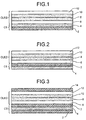
- FIG. 1 illustrates an organic light-emitting device with a composite structure as its substrate.
- OLED is used to denote the organic light-emitting device
- CS is used to denote the composite structure.
- the composite structure comprises a plastic layer 2 and a glass layer 4.
- the organic light-emitting device OLED comprises a first electrode layer 6, in this case an anode formed of indium tin oxide, a first thin film of an organic light emissive material 8 (in this case PPV), a second thin film of an organic material 10 (e.g. MEHPPV, and a second electrode layer 12 in this case a cathode, for example of a calcium layer capped by an aluminium layer.
- the second layer of organic material can be a light-emissive layer or a charge transport layer or have some other purpose. Further organic light-emissive layers can be provided.
- layer 8 could be a charge transport layer such as polyethylenedioxythiophene doped with polystyrene sulphonic acid (PEDT:PSS), polyaniline or PPV
- the second thin film layer 10 may be the light-emissive layer such as a blend of 5% poly(2,7-(9,9-di-n-octylfluorene)-3,6-(benzothiadiazole) with 95% poly(2,7-(9,9-di-n-octylfluorene) (5F8BT), poly(2,7-(9,9-di-n-octylfluorene) (F8), poly(2,7-(9,9-di-n-octylfluorene)-(1,4-phenylene- ((4-methylphenyl)imino)-1,4-phenylene-( (4-methylphenyl) imino)-1, 4-phenylene)
- the layer 12 forming the cathode can, for example, be a metallic element or alloy with a work function of typically less than or around 3.5 eV or preferably even less than or around 3 eV.
- Examples are Ca, Ba, Li, Sm, Yb, Tb, etc or alloys of Al, Ag or others with low work function elements such as Ca, Ba, Li, Sm, Yb, Tb, etc.
- the device of Figure 1 is constructed by first forming the composite structure CS.
- a laminate comprising the plastic layer 2 and glass layer 4 is first formed and then used as a substrate for deposition of the indium tin oxide layer 6 on top of the inner surface of the glass layer 4.
- the composite structure comprising the plastic layer 2 and glass layer 4 is first formed by laminating together a plastic sheet and a glass sheet.
- the glass sheet preferably has a thickness of around 200 ⁇ m and the plastic sheet has a thickness of around 200 ⁇ m.
- a layer of indium tin oxide 6 is deposited on the inner surface of the glass layer 4.
- an electroluminescent layer of poly(phenylene vinylene) (PPV) is deposited by spin-coating a precursor to PPV in a suitable solvent onto the ITO layer 6 and then heating the spin-coated layer to convert the precursor to the polymer PPV.
- a subsequent electroluminescent layer or charge transport layer 10 is put down in a similar fashion.
- a layer of Ca is evaporated followed by the evaporation of an Al capping layer.
- these layers could be deposited by sputtering, sequentially or by sputtering a Ca/Al alloy directly.
- the structure of Figure 1 is formed by a process in which the sequence of steps is varied.
- the layer of glass 4 Prior to forming the composite structure CS, the layer of glass 4 is coated on its surface with a layer of indium tin oxide 6 and, after that process, the plastic layer 2 is laminated to the underside of the glass layer 4. Subsequent steps for manufacture of the device are as described above with reference to the first embodiment.
- Figure 2 represents a different structure in accordance with the invention.
- the composite structure still comprises a layer of plastic 2 and a layer of glass 4, but these layers are now positioned with the glass layer being the outer layer of the device and the plastic layer being the inner layer.
- the construction of the device is as described earlier with reference to Figure 1.
- the device can be manufactured as already mentioned.
- Figure 3 illustrates a further different structure according to another embodiment of the invention.
- the composite structure comprises three layers, consisting of two plastic layers 2 and an intermediate glass layer 4.
- Manufacture of the device according to Figure 3 can be according to any of the preceding methods, that is by preformation of the composite structure and subsequent deposition of the organic light-emitting device layers, or by some intermediate coating step and subsequent laminating steps to form the composite structure.
- the structure of Figure 3 also includes an upper encapsulation layer 14 which encloses the cathode layer 12.
- the upper encapsulation layer 14 can similarly be used in the embodiments of Figures 1 and 2.
- the upper encapsulation layer 14 can be of the type already mentioned or can be a film/composite which has metal as the dominant barrier film, e.g. a metal foil or metal covered plastic foil.
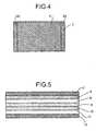
- Figure 4 illustrates a view looking down on the device, in which the plastic layer 2 of the composite extends slightly beyond the glass layer 4. This provides plastic strips 2a, 2b which allow the device to be picked up thus reducing the likelihood of cracking the glass layer.
- Figure 5 illustrates a device structure which has been fabricated in "reverse" order. That is, a metal encapsulation layer 14 forms the basis for deposition of the subsequent layers.
- like numerals denote like layers as in Figures 1 to 3.
- the lower encapsulation layer 14 can be replaced by an encapsulation layer having the following structures:
- the upper polymer layer 8 in Figure 5 can be a conducting polymer such as PEDT:PSS constituting a charge transport layer. It is possible to manufacture the device of Figure 5 by precoating a composite structure of a thin glass layer 4 and plastic layer 2 with a layer of ITO 6 and a layer of conducting polymer. That composite can then be laminated to a preformed structure comprising the metal layer 14, cathode layer 12 and polymer layer 10.
- a conducting polymer such as PEDT:PSS constituting a charge transport layer.
Landscapes
- Physics & Mathematics (AREA)
- Optics & Photonics (AREA)
- Electroluminescent Light Sources (AREA)
- Laminated Bodies (AREA)
- Devices For Indicating Variable Information By Combining Individual Elements (AREA)
Priority Applications (1)
| Application Number | Priority Date | Filing Date | Title |
|---|---|---|---|
| EP04076051.4A EP1439741B1 (en) | 1998-04-02 | 1999-03-31 | Flexible substrates for organic devices |
Applications Claiming Priority (2)
| Application Number | Priority Date | Filing Date | Title |
|---|---|---|---|
| GB9807149 | 1998-04-02 | ||
| GB9807149A GB2335884A (en) | 1998-04-02 | 1998-04-02 | Flexible substrates for electronic or optoelectronic devices |
Related Child Applications (1)
| Application Number | Title | Priority Date | Filing Date |
|---|---|---|---|
| EP04076051.4A Division EP1439741B1 (en) | 1998-04-02 | 1999-03-31 | Flexible substrates for organic devices |
Publications (2)
| Publication Number | Publication Date |
|---|---|
| EP0949850A1 EP0949850A1 (en) | 1999-10-13 |
| EP0949850B1 true EP0949850B1 (en) | 2004-08-04 |
Family
ID=10829786
Family Applications (2)
| Application Number | Title | Priority Date | Filing Date |
|---|---|---|---|
| EP99302512A Expired - Lifetime EP0949850B1 (en) | 1998-04-02 | 1999-03-31 | Flexible substrates for electronic or optoelectronic devices |
| EP04076051.4A Expired - Lifetime EP1439741B1 (en) | 1998-04-02 | 1999-03-31 | Flexible substrates for organic devices |
Family Applications After (1)
| Application Number | Title | Priority Date | Filing Date |
|---|---|---|---|
| EP04076051.4A Expired - Lifetime EP1439741B1 (en) | 1998-04-02 | 1999-03-31 | Flexible substrates for organic devices |
Country Status (5)
| Country | Link |
|---|---|
| US (3) | US6592969B1 (enExample) |
| EP (2) | EP0949850B1 (enExample) |
| JP (3) | JPH11329715A (enExample) |
| DE (1) | DE69919062T2 (enExample) |
| GB (1) | GB2335884A (enExample) |
Cited By (10)
| Publication number | Priority date | Publication date | Assignee | Title |
|---|---|---|---|---|
| US7326653B2 (en) | 2002-03-27 | 2008-02-05 | Cambridge Display Technology Limited | Method of preparation of organic optoelectronic and electronic devices and devices thereby obtained |
| US7510885B2 (en) | 2002-12-20 | 2009-03-31 | Cambridge Display Technology Limited | Method of preparing electronically connected optoelectronic devices, and optoelectronic devices |
| US7531831B2 (en) | 2003-03-20 | 2009-05-12 | Cambridge Display Technology Limited | Electroluminescent device comprising a cross-linked hole transporting and electron blocking material |
| US7531377B2 (en) | 2002-09-03 | 2009-05-12 | Cambridge Display Technology Limited | Optical device |
| US7745817B2 (en) | 2002-07-03 | 2010-06-29 | Cambridge Display Technology Limited | Combined information display and information input device |
| US8367798B2 (en) | 2008-09-29 | 2013-02-05 | The Regents Of The University Of California | Active materials for photoelectric devices and devices that use the materials |
| US8372945B2 (en) | 2009-07-24 | 2013-02-12 | Solarmer Energy, Inc. | Conjugated polymers with carbonyl substituted thieno[3,4-B]thiophene units for polymer solar cell active layer materials |
| CN103608927A (zh) * | 2011-06-15 | 2014-02-26 | 陶氏环球技术有限责任公司 | 柔性光伏制品 |
| US9136477B2 (en) | 2005-12-23 | 2015-09-15 | Cdt Oxford Limited | Light emissive device |
| US10276811B2 (en) | 2007-05-21 | 2019-04-30 | Corning Incorporated | Mechanically flexible and durable substrates and method of making |
Families Citing this family (209)
| Publication number | Priority date | Publication date | Assignee | Title |
|---|---|---|---|---|
| GB2335884A (en) * | 1998-04-02 | 1999-10-06 | Cambridge Display Tech Ltd | Flexible substrates for electronic or optoelectronic devices |
| WO2000006665A1 (en) * | 1998-07-28 | 2000-02-10 | The Dow Chemical Company | Organic electroluminescent devices |
| DE69827649T2 (de) * | 1998-12-21 | 2005-12-01 | Chi Mei Optoelectronics Corp. | Elektrisch leitfähiges Verbundglas |
| EP1048628A1 (de) | 1999-04-30 | 2000-11-02 | Schott Glas | Polymerbeschichtete Dünnglasfoliensubstrate |
| EP1186065A1 (en) * | 1999-04-28 | 2002-03-13 | E.I. Du Pont De Nemours And Company | Flexible organic electronic device with improved resistance to oxygen and moisture degradation |
| CA2342363A1 (en) * | 1999-07-09 | 2001-01-18 | Institute Of Materials Research & Engineering | Laminates for encapsulating devices |
| CN1218407C (zh) | 1999-07-09 | 2005-09-07 | 奥斯兰姆奥普托半导体股份有限两合公司 | 器件封装 |
| US6866901B2 (en) | 1999-10-25 | 2005-03-15 | Vitex Systems, Inc. | Method for edge sealing barrier films |
| US20100330748A1 (en) | 1999-10-25 | 2010-12-30 | Xi Chu | Method of encapsulating an environmentally sensitive device |
| US6623861B2 (en) | 2001-04-16 | 2003-09-23 | Battelle Memorial Institute | Multilayer plastic substrates |
| US7198832B2 (en) | 1999-10-25 | 2007-04-03 | Vitex Systems, Inc. | Method for edge sealing barrier films |
| US6413645B1 (en) | 2000-04-20 | 2002-07-02 | Battelle Memorial Institute | Ultrabarrier substrates |
| GB9928014D0 (en) * | 1999-11-26 | 2000-01-26 | Cambridge Display Tech Ltd | Method of producing an organic light-emissive device |
| DE19959084B4 (de) * | 1999-12-08 | 2005-05-12 | Schott Ag | Organisches LED-Display und Verfahren zu seiner Herstellung |
| TW480727B (en) | 2000-01-11 | 2002-03-21 | Semiconductor Energy Laboratro | Semiconductor display device |
| DE10045204A1 (de) * | 2000-09-13 | 2002-04-04 | Siemens Ag | Träger für eine OLED und Verfahren zur Herstellung eines Trägers für eine OLED |
| JP4491942B2 (ja) * | 2000-09-19 | 2010-06-30 | 凸版印刷株式会社 | エレクトロルミネッセンス素子およびその製造方法 |
| KR100359296B1 (ko) * | 2000-10-14 | 2002-11-07 | 삼성에스디아이 주식회사 | 유기 전계발광 디바이스 및 이의 제조 방법 |
| JP2002313558A (ja) * | 2001-04-13 | 2002-10-25 | Toppan Printing Co Ltd | 有機エレクトロルミネッセンス表示素子及びその製造方法 |
| US7211950B2 (en) * | 2001-05-29 | 2007-05-01 | Choong Hoon Yi | Organic electro luminescent display and manufacturing method thereof |
| JP2003036974A (ja) * | 2001-07-23 | 2003-02-07 | Victor Co Of Japan Ltd | 有機エレクトロルミネッセンス素子及びその製造方法 |
| CN102785419B (zh) * | 2001-09-11 | 2015-01-14 | 美国杜邦泰津胶片合伙人有限公司 | 用于柔性电子器件和光电子器件的热稳定聚萘二甲酸乙二醇酯膜 |
| JP2003140561A (ja) | 2001-10-30 | 2003-05-16 | Seiko Epson Corp | 電気光学装置及びその製造方法並びに電子機器 |
| JP4071652B2 (ja) | 2002-03-04 | 2008-04-02 | 株式会社 日立ディスプレイズ | 有機el発光表示装置 |
| JP2003308968A (ja) * | 2002-04-12 | 2003-10-31 | Rohm Co Ltd | エレクトロルミネッセンス発光素子及びその製法 |
| US8900366B2 (en) | 2002-04-15 | 2014-12-02 | Samsung Display Co., Ltd. | Apparatus for depositing a multilayer coating on discrete sheets |
| US8808457B2 (en) | 2002-04-15 | 2014-08-19 | Samsung Display Co., Ltd. | Apparatus for depositing a multilayer coating on discrete sheets |
| US6787990B2 (en) | 2002-05-28 | 2004-09-07 | Eastman Kodak Company | OLED area illumination light source having flexible substrate on a support |
| EP1416028A1 (en) | 2002-10-30 | 2004-05-06 | Covion Organic Semiconductors GmbH | New method for the production of monomers useful in the manufacture of semiconductive polymers |
| GB0226010D0 (en) | 2002-11-08 | 2002-12-18 | Cambridge Display Tech Ltd | Polymers for use in organic electroluminescent devices |
| US6982179B2 (en) * | 2002-11-15 | 2006-01-03 | University Display Corporation | Structure and method of fabricating organic devices |
| US20040096570A1 (en) * | 2002-11-15 | 2004-05-20 | Michael Weaver | Structure and method of fabricating organic devices |
| US7011983B2 (en) * | 2002-12-20 | 2006-03-14 | General Electric Company | Large organic devices and methods of fabricating large organic devices |
| JP2004207078A (ja) * | 2002-12-25 | 2004-07-22 | Seiko Epson Corp | 表示パネルおよびその製造方法 |
| JP4063082B2 (ja) * | 2003-01-10 | 2008-03-19 | 日本電気株式会社 | フレキシブル電子デバイスとその製造方法 |
| US6790594B1 (en) * | 2003-03-20 | 2004-09-14 | Eastman Kodak Company | High absorption donor substrate coatable with organic layer(s) transferrable in response to incident laser light |
| US7510913B2 (en) | 2003-04-11 | 2009-03-31 | Vitex Systems, Inc. | Method of making an encapsulated plasma sensitive device |
| US7648925B2 (en) | 2003-04-11 | 2010-01-19 | Vitex Systems, Inc. | Multilayer barrier stacks and methods of making multilayer barrier stacks |
| GB0311234D0 (en) | 2003-05-16 | 2003-06-18 | Isis Innovation | Organic phosphorescent material and organic optoelectronic device |
| JP2007504342A (ja) | 2003-05-30 | 2007-03-01 | メルク パテント ゲーエムベーハー | ポリマー |
| DE10328140B4 (de) * | 2003-06-20 | 2006-12-07 | Schott Ag | Organische lichtemittierende Einrichtung und Verfahren zu deren Herstellung |
| EP1491568A1 (en) | 2003-06-23 | 2004-12-29 | Covion Organic Semiconductors GmbH | Semiconductive Polymers |
| GB0322686D0 (en) | 2003-09-27 | 2003-10-29 | Koninkl Philips Electronics Nv | Display device arrangement & container |
| KR100781423B1 (ko) * | 2003-11-13 | 2007-12-03 | 스미토모 쇼지 가부시키가이샤 | 연성 기판 및 코팅액 |
| GB0329364D0 (en) | 2003-12-19 | 2004-01-21 | Cambridge Display Tech Ltd | Optical device |
| WO2005096675A1 (ja) * | 2004-03-31 | 2005-10-13 | Pioneer Corporation | 発光パネルの製造方法 |
| JP2005297498A (ja) * | 2004-04-16 | 2005-10-27 | Dainippon Printing Co Ltd | 可撓性基板およびそれを用いた有機デバイス |
| KR20070024613A (ko) * | 2004-05-19 | 2007-03-02 | 디에스엠 아이피 어셋츠 비.브이. | 전자 광학 소자용 복합 적층 물질의 제조방법 |
| GB0411572D0 (en) | 2004-05-24 | 2004-06-23 | Cambridge Display Tech Ltd | Light-emitting device |
| GB0411582D0 (en) | 2004-05-24 | 2004-06-23 | Cambridge Display Tech Ltd | Metal complex |
| US20050269943A1 (en) * | 2004-06-04 | 2005-12-08 | Michael Hack | Protected organic electronic devices and methods for making the same |
| JP2006041135A (ja) * | 2004-07-26 | 2006-02-09 | Sumitomo Bakelite Co Ltd | 電子デバイスおよびその製造方法 |
| US20060022910A1 (en) * | 2004-07-30 | 2006-02-02 | Takuro Sekiya | Multifunction display device |
| EP1627891A1 (en) | 2004-08-11 | 2006-02-22 | Covion Organic Semiconductors GmbH | Polymers for use in organic electroluminescent devices |
| US9179518B2 (en) | 2004-12-24 | 2015-11-03 | Cambridge Display Technology Limited | Light emissive device |
| GB2436996B8 (en) | 2004-12-29 | 2013-12-11 | Cambridge Display Tech Ltd | Rigid amines |
| GB0428445D0 (en) | 2004-12-29 | 2005-02-02 | Cambridge Display Tech Ltd | Blue-shifted triarylamine polymer |
| GB0428444D0 (en) | 2004-12-29 | 2005-02-02 | Cambridge Display Tech Ltd | Conductive polymer compositions in opto-electrical devices |
| JP2006221892A (ja) * | 2005-02-09 | 2006-08-24 | Hitachi Displays Ltd | 表示装置 |
| GB0507684D0 (en) | 2005-04-15 | 2005-05-25 | Cambridge Display Tech Ltd | Pulsed driven displays |
| US20080109941A1 (en) * | 2005-05-26 | 2008-05-15 | Energy Integration Technologies, Inc. | Thin film energy fabric integration, control and method of making |
| US20110127248A1 (en) * | 2005-05-26 | 2011-06-02 | Kinaptic,LLC | Thin film energy fabric for self-regulating heat generation layer |
| US20110130813A1 (en) * | 2005-05-26 | 2011-06-02 | Kinaptic, LLC | Thin film energy fabric for self-regulating heated wound dressings |
| US20110128726A1 (en) * | 2005-05-26 | 2011-06-02 | Kinaptic, LLC | Thin film energy fabric with light generation layer |
| US20110128686A1 (en) * | 2005-05-26 | 2011-06-02 | Kinaptic, LLC | Thin film energy fabric with energy transmission/reception layer |
| US20060278965A1 (en) * | 2005-06-10 | 2006-12-14 | Foust Donald F | Hermetically sealed package and methods of making the same |
| JP4982976B2 (ja) * | 2005-06-29 | 2012-07-25 | 住友化学株式会社 | フレキシブル基板の製造方法及びディスプレイ素子 |
| WO2007004131A2 (en) * | 2005-06-30 | 2007-01-11 | Polymer Vision Limited | Bagged rollable display |
| GB0514476D0 (en) | 2005-07-14 | 2005-08-17 | Cambridge Display Tech Ltd | Conductive polymer compositions in opto-electrical devices |
| US7767498B2 (en) | 2005-08-25 | 2010-08-03 | Vitex Systems, Inc. | Encapsulated devices and method of making |
| GB0518968D0 (en) | 2005-09-16 | 2005-10-26 | Cdt Oxford Ltd | Organic light-emitting device |
| KR100639919B1 (ko) * | 2005-10-10 | 2006-11-01 | 한국전자통신연구원 | 섬유강화 플라스틱 기판의 표면 처리 방법 |
| GB2432256B (en) | 2005-11-14 | 2009-12-23 | Cambridge Display Tech Ltd | Organic optoelectrical device |
| WO2007087016A2 (en) * | 2005-12-08 | 2007-08-02 | Stuart Weissman | Surface-mounted contour-fitting electronic visual display system for use on vehicles and other objects |
| GB2433509A (en) | 2005-12-22 | 2007-06-27 | Cambridge Display Tech Ltd | Arylamine polymer |
| GB0526185D0 (en) | 2005-12-22 | 2006-02-01 | Cambridge Display Tech Ltd | Electronic device |
| US7463734B2 (en) * | 2006-02-03 | 2008-12-09 | Sony Ericsson Mobile Communications Ab | Display window cover assemblies and electronic devices and methods using the same |
| JP5209504B2 (ja) * | 2006-02-08 | 2013-06-12 | スリーエム イノベイティブ プロパティズ カンパニー | ガラス転移点を超える温度でのフィルム基材の製造のための方法 |
| US7791271B2 (en) * | 2006-02-24 | 2010-09-07 | Global Oled Technology Llc | Top-emitting OLED device with light-scattering layer and color-conversion |
| GB2440934B (en) | 2006-04-28 | 2009-12-16 | Cdt Oxford Ltd | Opto-electrical polymers and devices |
| DE102006059129A1 (de) * | 2006-07-31 | 2008-02-07 | Osram Opto Semiconductors Gmbh | Strahlungsemittierendes Bauelement |
| GB0617167D0 (en) | 2006-08-31 | 2006-10-11 | Cdt Oxford Ltd | Compounds for use in opto-electrical devices |
| GB0620045D0 (en) | 2006-10-10 | 2006-11-22 | Cdt Oxford Ltd | Otpo-electrical devices and methods of making the same |
| JP2008107510A (ja) * | 2006-10-25 | 2008-05-08 | Nitto Denko Corp | 表示素子用基板およびその製造方法 |
| US20080145602A1 (en) * | 2006-12-15 | 2008-06-19 | Gary Lee Hendren | Processes for making shaped honeycomb and honeycombs made thereby |
| WO2008111481A1 (ja) * | 2007-03-12 | 2008-09-18 | Konica Minolta Medical & Graphic, Inc. | 放射線像変換パネル |
| JP4845129B2 (ja) * | 2007-03-28 | 2011-12-28 | 国立大学法人京都大学 | フレキシブル基板およびその製造方法 |
| GB2448175B (en) | 2007-04-04 | 2009-07-22 | Cambridge Display Tech Ltd | Thin film transistor |
| WO2009017700A1 (en) * | 2007-07-27 | 2009-02-05 | The Regents Of The University Of California | Polymer electronic devices by all-solution process |
| JP4621713B2 (ja) * | 2007-08-06 | 2011-01-26 | 株式会社東芝 | アクティブマトリクス型表示装置 |
| JP4550871B2 (ja) * | 2007-08-06 | 2010-09-22 | 株式会社東芝 | アクティブマトリクス型表示装置 |
| JP2009094050A (ja) * | 2007-09-19 | 2009-04-30 | Fujifilm Corp | 発光素子または表示素子、およびこれらの製造方法 |
| US8033882B2 (en) * | 2007-09-19 | 2011-10-11 | Fujifilm Corporation | Light-emitting device or display device, and method for producing them |
| GB2454890B (en) | 2007-11-21 | 2010-08-25 | Limited Cambridge Display Technology | Light-emitting device and materials therefor |
| GB2455747B (en) | 2007-12-19 | 2011-02-09 | Cambridge Display Tech Ltd | Electronic devices and methods of making the same using solution processing techniques |
| GB2456788B (en) | 2008-01-23 | 2011-03-09 | Cambridge Display Tech Ltd | White light emitting material |
| TWI369916B (en) * | 2008-01-31 | 2012-08-01 | Ind Tech Res Inst | Top emitting oled display and fabrication method thereof |
| JP4990182B2 (ja) * | 2008-02-21 | 2012-08-01 | 株式会社アイテス | 有機elパネルのリペア装置およびリペア方法 |
| GB0803950D0 (en) | 2008-03-03 | 2008-04-09 | Cambridge Display Technology O | Solvent for printing composition |
| US20090229667A1 (en) * | 2008-03-14 | 2009-09-17 | Solarmer Energy, Inc. | Translucent solar cell |
| GB2458454B (en) | 2008-03-14 | 2011-03-16 | Cambridge Display Tech Ltd | Electronic devices and methods of making the same using solution processing techniques |
| JP5296410B2 (ja) * | 2008-04-23 | 2013-09-25 | 日東電工株式会社 | 素子作製工程用基板 |
| JP5439019B2 (ja) * | 2008-04-24 | 2014-03-12 | 日東電工株式会社 | 表示素子用基板およびその製造方法 |
| JP5467792B2 (ja) * | 2008-04-24 | 2014-04-09 | 日東電工株式会社 | 可撓性基板 |
| KR101374400B1 (ko) * | 2008-04-24 | 2014-03-17 | 닛토덴코 가부시키가이샤 | 투명 기판 |
| JP5142382B2 (ja) * | 2008-04-24 | 2013-02-13 | 日東電工株式会社 | 太陽電池用基板、太陽電池素子、太陽電池用モジュールおよび太陽電池用基板の製造方法 |
| TWI370525B (en) * | 2008-04-25 | 2012-08-11 | Ind Tech Res Inst | Encapsulant composition and method for fabricating encapsulant material |
| GB2459895B (en) | 2008-05-09 | 2011-04-27 | Cambridge Display Technology Limited | Organic light emissive device |
| JP2008273211A (ja) * | 2008-05-19 | 2008-11-13 | Nitto Denko Corp | 透明ガスバリア性部材及びこれを用いた有機エレクトロルミネッセンス素子 |
| GB2462410B (en) | 2008-07-21 | 2011-04-27 | Cambridge Display Tech Ltd | Compositions and methods for manufacturing light-emissive devices |
| GB2462122B (en) | 2008-07-25 | 2013-04-03 | Cambridge Display Tech Ltd | Electroluminescent materials |
| GB2462314B (en) | 2008-08-01 | 2011-03-16 | Cambridge Display Tech Ltd | Organic light-emiting materials and devices |
| GB0814161D0 (en) | 2008-08-01 | 2008-09-10 | Cambridge Display Tech Ltd | Blue-light emitting material |
| JP5108675B2 (ja) * | 2008-08-12 | 2012-12-26 | 帝人デュポンフィルム株式会社 | 複合フィルム |
| GB2462844B (en) | 2008-08-21 | 2011-04-20 | Cambridge Display Tech Ltd | Organic electroluminescent device |
| GB2463040B (en) | 2008-08-28 | 2012-10-31 | Cambridge Display Tech Ltd | Light-emitting material |
| GB2463077B (en) | 2008-09-02 | 2012-11-07 | Sumitomo Chemical Co | Electroluminescent material and device |
| GB2464111B (en) | 2008-10-02 | 2011-06-15 | Cambridge Display Tech Ltd | Organic electroluminescent device |
| US20110244225A1 (en) | 2008-11-07 | 2011-10-06 | Nitto Denko Corporation | Transparent substrate and method for production thereof |
| EP2192636A1 (en) | 2008-11-26 | 2010-06-02 | Rijksuniversiteit Groningen | Modulatable light-emitting diode |
| GB2466251B (en) * | 2008-12-16 | 2011-03-09 | Ind Tech Res Inst | Encapsulant compositions and method for fabricating encapsulant materials |
| US9184410B2 (en) | 2008-12-22 | 2015-11-10 | Samsung Display Co., Ltd. | Encapsulated white OLEDs having enhanced optical output |
| US9337446B2 (en) | 2008-12-22 | 2016-05-10 | Samsung Display Co., Ltd. | Encapsulated RGB OLEDs having enhanced optical output |
| GB0823397D0 (en) * | 2008-12-23 | 2009-01-28 | Eastman Kodak Co | Multilayer devices on flexible supports |
| GB2466843A (en) | 2009-01-12 | 2010-07-14 | Cambridge Display Tech Ltd | Interlayer formulation for flat films |
| GB2466842B (en) | 2009-01-12 | 2011-10-26 | Cambridge Display Tech Ltd | Interlayer formulation for flat films |
| JP5297237B2 (ja) * | 2009-03-19 | 2013-09-25 | パナソニック株式会社 | 透明基板/ガラス板複合フィルムとその製造方法ならびにフレキシブル有機エレクトロルミネッセンス照明、フレキシブル太陽電池 |
| GB2469498B (en) | 2009-04-16 | 2012-03-07 | Cambridge Display Tech Ltd | Polymer and polymerisation method |
| GB2469500B (en) | 2009-04-16 | 2012-06-06 | Cambridge Display Tech Ltd | Method of forming a polymer |
| GB0906554D0 (en) | 2009-04-16 | 2009-05-20 | Cambridge Display Tech Ltd | Organic electroluminescent device |
| GB2469497B (en) | 2009-04-16 | 2012-04-11 | Cambridge Display Tech Ltd | Polymers comprising fluorene derivative repeat units and their preparation |
| US8418418B2 (en) | 2009-04-29 | 2013-04-16 | 3Form, Inc. | Architectural panels with organic photovoltaic interlayers and methods of forming the same |
| JP2010262897A (ja) * | 2009-05-11 | 2010-11-18 | Rohm Co Ltd | 有機半導体装置 |
| JP5330966B2 (ja) * | 2009-05-14 | 2013-10-30 | 日東電工株式会社 | 透明基板ならびに透明基板を用いた表示素子、太陽電池および照明素子 |
| US8440496B2 (en) | 2009-07-08 | 2013-05-14 | Solarmer Energy, Inc. | Solar cell with conductive material embedded substrate |
| US20110023548A1 (en) | 2009-07-29 | 2011-02-03 | Garner Sean M | Glass substrate comprising an edge web portion |
| DE102009038904A1 (de) | 2009-08-29 | 2011-03-10 | Bundesdruckerei Gmbh | Gegenstand mit einem Organic Light Emitting Display |
| JP2011082070A (ja) * | 2009-10-08 | 2011-04-21 | Dainippon Printing Co Ltd | 光学装置 |
| EP2374766A4 (en) * | 2009-10-09 | 2012-04-04 | Micro Technology Co Ltd | METHOD FOR PRODUCING A FLEXIBLE GLASS SUBSTRATE AND A FLEXIBLE GLASS SUBSTRATE |
| KR101811893B1 (ko) | 2009-10-22 | 2017-12-22 | 닛토덴코 가부시키가이샤 | 투명 기판 |
| JP5416546B2 (ja) | 2009-10-23 | 2014-02-12 | 日東電工株式会社 | 透明基板 |
| US8399889B2 (en) | 2009-11-09 | 2013-03-19 | Solarmer Energy, Inc. | Organic light emitting diode and organic solar cell stack |
| GB2475247B (en) | 2009-11-10 | 2012-06-13 | Cambridge Display Tech Ltd | Organic optoelectronic device and method |
| GB2475246B (en) | 2009-11-10 | 2012-02-29 | Cambridge Display Tech Ltd | Organic opto-electronic device and method |
| US8590338B2 (en) | 2009-12-31 | 2013-11-26 | Samsung Mobile Display Co., Ltd. | Evaporator with internal restriction |
| US8288187B2 (en) * | 2010-01-20 | 2012-10-16 | Universal Display Corporation | Electroluminescent devices for lighting applications |
| CN102782772A (zh) * | 2010-03-05 | 2012-11-14 | 卡尔斯特里姆保健公司 | 透明导电膜、制品及方法 |
| US9995831B2 (en) * | 2010-04-26 | 2018-06-12 | Koninklijke Philips N.V. | X-ray detector with improved spatial gain uniformity and resolution and method of fabricating such X-ray detector |
| JP5615134B2 (ja) | 2010-04-30 | 2014-10-29 | 日東電工株式会社 | 透明基板の製造方法 |
| GB2480323A (en) | 2010-05-14 | 2011-11-16 | Cambridge Display Tech Ltd | OLED hole transport layer |
| GB2487342B (en) | 2010-05-14 | 2013-06-19 | Cambridge Display Tech Ltd | Host polymer comprising conjugated repeat units and non-conjugated repeat units for light-emitting compositions, and organic light-emitting devices |
| GB2484253B (en) | 2010-05-14 | 2013-09-11 | Cambridge Display Tech Ltd | Organic light-emitting composition and device |
| GB2499969A (en) | 2010-06-25 | 2013-09-11 | Cambridge Display Tech Ltd | Composition comprising an organic semiconducting material and a triplet-accepting material |
| CN102959758B (zh) | 2010-06-25 | 2016-03-23 | 剑桥显示技术有限公司 | 有机发光材料、器件和方法 |
| GB2483269A (en) | 2010-09-02 | 2012-03-07 | Cambridge Display Tech Ltd | Organic Electroluminescent Device containing Fluorinated Compounds |
| GB2484537A (en) | 2010-10-15 | 2012-04-18 | Cambridge Display Tech Ltd | Light-emitting composition |
| GB2485001A (en) | 2010-10-19 | 2012-05-02 | Cambridge Display Tech Ltd | OLEDs |
| US20120192928A1 (en) * | 2011-01-27 | 2012-08-02 | Mark Francis Krol | Laminated pv module package |
| KR101911971B1 (ko) | 2011-01-31 | 2018-10-25 | 캠브리지 디스플레이 테크놀로지 리미티드 | 중합체 |
| GB2494096B (en) | 2011-01-31 | 2013-12-18 | Cambridge Display Tech Ltd | Polymer |
| US8227962B1 (en) | 2011-03-09 | 2012-07-24 | Allen Hui Long Su | LED light bulb having an LED light engine with illuminated curved surfaces |
| JP5688182B2 (ja) * | 2011-03-30 | 2015-03-25 | オーシャンズ キング ライティング サイエンスアンドテクノロジー カンパニー リミテッド | フレキシブル有機エレクトロルミネッセンスデバイス及びその製造方法 |
| GB201105582D0 (en) | 2011-04-01 | 2011-05-18 | Cambridge Display Tech Ltd | Organic light-emitting device and method |
| JP5724554B2 (ja) * | 2011-04-04 | 2015-05-27 | Jsr株式会社 | 発光素子および発光素子形成用樹脂組成物 |
| GB201107905D0 (en) | 2011-05-12 | 2011-06-22 | Cambridge Display Tech Ltd | Light-emitting material, composition and device |
| US9034458B2 (en) * | 2011-05-27 | 2015-05-19 | Corning Incorporated | Edge-protected product and finishing method |
| TWI547369B (zh) | 2011-05-27 | 2016-09-01 | 康寧公司 | 玻璃塑膠積層之裝置、處理線、及方法 |
| GB201110565D0 (en) | 2011-06-22 | 2011-08-03 | Cambridge Display Tech Ltd | Organic optoelectronic material, device and method |
| WO2013000797A1 (de) * | 2011-06-30 | 2013-01-03 | Osram Opto Semiconductors Gmbh | Verkapselungsstruktur für ein optoelektronisches bauelement und verfahren zum verkapseln eines optoelektronischen bauelementes |
| DE102011079160B4 (de) | 2011-07-14 | 2023-05-17 | Osram Oled Gmbh | Verkapselungsstruktur für ein optoelektronisches bauelement und verfahren zum verkapseln eines optoelektronischen bauelements |
| US9493613B2 (en) | 2011-07-04 | 2016-11-15 | Cambridge Display Technology, Ltd. | Organic light emitting composition, device and method |
| GB201111742D0 (en) | 2011-07-08 | 2011-08-24 | Cambridge Display Tech Ltd | Solution |
| WO2013007592A1 (de) * | 2011-07-14 | 2013-01-17 | Osram Opto Semiconductors Gmbh | Verkapselungsstruktur für ein optoelektronisches bauelement und verfahren zum verkapseln eines optoelektronischen bauelementes |
| GB201210131D0 (en) | 2011-11-02 | 2012-07-25 | Cambridge Display Tech Ltd | Light emitting composition and device |
| GB201118997D0 (en) | 2011-11-03 | 2011-12-14 | Cambridge Display Tech Ltd | Electronic device and method |
| CN104093689A (zh) | 2012-01-31 | 2014-10-08 | 剑桥显示技术有限公司 | 聚合物 |
| WO2013118508A1 (ja) * | 2012-02-07 | 2013-08-15 | パナソニック株式会社 | 複合基板及びその製造方法、並びに、有機エレクトロルミネッセンス素子 |
| JP2013186984A (ja) * | 2012-03-07 | 2013-09-19 | Panasonic Corp | 複合基板構造及びその作製方法、並びに、有機エレクトロルミネッセンス素子 |
| JP2012134544A (ja) * | 2012-03-09 | 2012-07-12 | Nitto Denko Corp | 太陽電池用基板、太陽電池素子、太陽電池用モジュールおよび太陽電池用基板の製造方法 |
| JP5883333B2 (ja) * | 2012-04-02 | 2016-03-15 | 日東電工株式会社 | 透明シートおよびその製造方法 |
| WO2013180134A1 (ja) | 2012-05-29 | 2013-12-05 | 日東電工株式会社 | 接着剤およびそれを用いた透明基板 |
| KR20150027067A (ko) | 2012-05-29 | 2015-03-11 | 닛토덴코 가부시키가이샤 | 접착제 및 그것을 사용한 투명 기판 |
| JP2012247785A (ja) * | 2012-07-04 | 2012-12-13 | Nitto Denko Corp | 表示素子用基板およびその製造方法 |
| US20140014260A1 (en) | 2012-07-12 | 2014-01-16 | Dipakbin Qasem Chowdhury | Laminated structures and methods of manufacturing laminated structures |
| KR20150042778A (ko) * | 2012-08-09 | 2015-04-21 | 아사히 가라스 가부시키가이샤 | 유리 시트 불소 수지 적층체 |
| TW201412521A (zh) * | 2012-08-09 | 2014-04-01 | Asahi Glass Co Ltd | 玻璃片積層體及玻璃片積層體之製造方法 |
| KR101963810B1 (ko) * | 2012-08-22 | 2019-04-02 | 삼성디스플레이 주식회사 | 유기 발광 디스플레이 장치 |
| KR20140063303A (ko) * | 2012-11-16 | 2014-05-27 | 삼성디스플레이 주식회사 | 플렉서블 디스플레이 장치의 제조 방법 |
| US9504124B2 (en) * | 2013-01-03 | 2016-11-22 | Apple Inc. | Narrow border displays for electronic devices |
| JP6278480B2 (ja) | 2013-01-07 | 2018-02-14 | コーニング インコーポレイテッド | 強化合わせガラス構造 |
| JP2014159352A (ja) * | 2013-02-20 | 2014-09-04 | Nitto Denko Corp | 可撓性フィルムの製造方法 |
| KR101924772B1 (ko) | 2013-03-08 | 2018-12-04 | 파이오니아 가부시키가이샤 | 발광 소자 |
| US9321677B2 (en) | 2014-01-29 | 2016-04-26 | Corning Incorporated | Bendable glass stack assemblies, articles and methods of making the same |
| TWI699023B (zh) * | 2014-06-30 | 2020-07-11 | 日商半導體能源研究所股份有限公司 | 發光裝置,模組,及電子裝置 |
| JP6592883B2 (ja) * | 2014-08-06 | 2019-10-23 | 三菱ケミカル株式会社 | 有機el素子及びそれを用いた有機el照明装置 |
| WO2016020498A1 (de) * | 2014-08-07 | 2016-02-11 | Ceramtec-Etec Gmbh | Kantenbruchsicheres sichtfenster |
| DE102014114453A1 (de) * | 2014-10-06 | 2016-04-07 | Sabine Rinke | Mehrschichtkörper |
| DE102014221245A1 (de) | 2014-10-20 | 2016-04-21 | Tesa Se | Dünnglasfolienverbundbahn mit Versteifungsstreifen |
| US20170024062A1 (en) * | 2015-07-21 | 2017-01-26 | Panasonic Avionics Corporation | Scratch resistant layer of ultra-thin glass on a substrate for touch sensitive display |
| KR102639302B1 (ko) * | 2015-10-15 | 2024-02-21 | 삼성디스플레이 주식회사 | 표시 패널 및 표시 패널의 제조 방법 |
| CN109155374A (zh) * | 2016-04-29 | 2019-01-04 | 沙特基础工业全球技术公司 | 提取衬底及其制造方法 |
| KR102696454B1 (ko) * | 2016-12-02 | 2024-08-22 | 삼성디스플레이 주식회사 | 저곡률로 굽힘이 가능한 플렉시블 글라스 물품 및 그 제조 방법 |
| CN207571423U (zh) * | 2017-08-28 | 2018-07-03 | 惠科股份有限公司 | 显示面板 |
| JP6790008B2 (ja) * | 2018-03-14 | 2020-11-25 | 株式会社東芝 | 検出素子および検出器 |
| KR102622861B1 (ko) * | 2018-06-22 | 2024-01-10 | 삼성디스플레이 주식회사 | 연성 기판 및 이를 포함하는 표시 장치 |
| GB2575089A (en) | 2018-06-28 | 2020-01-01 | Sumitomo Chemical Co | Phosphorescent light-emitting compound |
| JP2019035986A (ja) * | 2018-11-22 | 2019-03-07 | 株式会社半導体エネルギー研究所 | 電子機器の作製方法 |
| CN110854300B (zh) * | 2019-11-27 | 2024-09-13 | 京东方科技集团股份有限公司 | 显示装置、显示面板及其制造方法 |
| DE102020205028A1 (de) * | 2020-04-21 | 2021-10-21 | Implanta Beteiligungs-GmbH | Mehrlagiger Schutzglasverbund, Anzeigevorrichtung mit einem formflexiblen Anzeigeelement und einem daran befestigten derartigen Schutzglasverbund sowie Verwendung einer Dünnglaslage als Schutzglas |
Family Cites Families (22)
| Publication number | Priority date | Publication date | Assignee | Title |
|---|---|---|---|---|
| US3777222A (en) * | 1972-05-12 | 1973-12-04 | Ibm | Modular touch sensitive indicating panels with touch and light transmissive overlay cover membrane containing visible printed indicia |
| GB1461255A (en) * | 1972-11-09 | 1977-01-13 | Ici Ltd | Laminating process |
| US4318958A (en) * | 1979-03-19 | 1982-03-09 | The United States Of America As Represented By The Secretary Of The Army | Flexible, high contrast, non-glare, polarizing filter for an illuminated switch assembly |
| US4539507A (en) | 1983-03-25 | 1985-09-03 | Eastman Kodak Company | Organic electroluminescent devices having improved power conversion efficiencies |
| US4600640A (en) * | 1984-08-13 | 1986-07-15 | General Electric Company | Thermoplastic resinous substrates having an external thin glass sheet protective layer |
| JPS6314393Y2 (enExample) * | 1985-05-30 | 1988-04-22 | ||
| GB8712057D0 (en) * | 1987-05-21 | 1987-06-24 | British Petroleum Co Plc | Optical modulators |
| GB8909011D0 (en) | 1989-04-20 | 1989-06-07 | Friend Richard H | Electroluminescent devices |
| BR9306230A (pt) * | 1993-02-11 | 1998-06-30 | Ericsson Telefon Ab L M | Dispositivo para encerrar flexivelmente um conjunto circuito eletrônico |
| JP3059866B2 (ja) * | 1993-07-30 | 2000-07-04 | シャープ株式会社 | 表示装置用基板 |
| US5482896A (en) * | 1993-11-18 | 1996-01-09 | Eastman Kodak Company | Light emitting device comprising an organic LED array on an ultra thin substrate and process for forming same |
| GB9507862D0 (en) * | 1995-04-18 | 1995-05-31 | Cambridge Display Tech Ltd | Fabrication of organic light-emitting devices |
| KR100500078B1 (ko) * | 1996-02-26 | 2005-07-18 | 이데미쓰 고산 가부시키가이샤 | 유기 전자 발광 소자 및 그의 제조방법 |
| TW446637B (en) * | 1996-05-28 | 2001-07-21 | Mitsui Chemicals Inc | Transparent laminates and optical filters for displays using the same |
| JPH10106746A (ja) * | 1996-09-27 | 1998-04-24 | Pioneer Electron Corp | エレクトロルミネセンス素子及びエレクトロルミネセンス素子の製造方法 |
| US6287674B1 (en) | 1997-10-24 | 2001-09-11 | Agfa-Gevaert | Laminate comprising a thin borosilicate glass substrate as a constituting layer |
| WO1999021707A1 (en) | 1997-10-24 | 1999-05-06 | Agfa-Gevaert Naamloze Vennootschap | A laminate comprising a thin borosilicate glass substrate as a constituting layer |
| EP0948004A1 (en) * | 1998-03-26 | 1999-10-06 | Akzo Nobel N.V. | Method for making a photovoltaic cell containing a dye |
| GB2335884A (en) * | 1998-04-02 | 1999-10-06 | Cambridge Display Tech Ltd | Flexible substrates for electronic or optoelectronic devices |
| DE69926112T2 (de) | 1998-07-20 | 2006-05-11 | Koninklijke Philips Electronics N.V. | Flexibles substrat |
| US6197418B1 (en) * | 1998-12-21 | 2001-03-06 | Agfa-Gevaert, N.V. | Electroconductive glass laminate |
| EP1048628A1 (de) | 1999-04-30 | 2000-11-02 | Schott Glas | Polymerbeschichtete Dünnglasfoliensubstrate |
-
1998
- 1998-04-02 GB GB9807149A patent/GB2335884A/en not_active Withdrawn
-
1999
- 1999-03-31 EP EP99302512A patent/EP0949850B1/en not_active Expired - Lifetime
- 1999-03-31 DE DE69919062T patent/DE69919062T2/de not_active Expired - Lifetime
- 1999-03-31 EP EP04076051.4A patent/EP1439741B1/en not_active Expired - Lifetime
- 1999-04-01 US US09/283,424 patent/US6592969B1/en not_active Expired - Lifetime
- 1999-04-02 JP JP11097047A patent/JPH11329715A/ja active Pending
-
2002
- 2002-12-24 US US10/326,977 patent/US6994906B2/en not_active Expired - Lifetime
-
2006
- 2006-02-06 US US11/347,866 patent/US7514866B2/en not_active Expired - Fee Related
-
2007
- 2007-07-24 JP JP2007192528A patent/JP4577852B2/ja not_active Expired - Lifetime
-
2008
- 2008-04-01 JP JP2008095403A patent/JP4332579B2/ja not_active Expired - Lifetime
Cited By (14)
| Publication number | Priority date | Publication date | Assignee | Title |
|---|---|---|---|---|
| US7326653B2 (en) | 2002-03-27 | 2008-02-05 | Cambridge Display Technology Limited | Method of preparation of organic optoelectronic and electronic devices and devices thereby obtained |
| US7745817B2 (en) | 2002-07-03 | 2010-06-29 | Cambridge Display Technology Limited | Combined information display and information input device |
| US7531377B2 (en) | 2002-09-03 | 2009-05-12 | Cambridge Display Technology Limited | Optical device |
| US7510885B2 (en) | 2002-12-20 | 2009-03-31 | Cambridge Display Technology Limited | Method of preparing electronically connected optoelectronic devices, and optoelectronic devices |
| US7531831B2 (en) | 2003-03-20 | 2009-05-12 | Cambridge Display Technology Limited | Electroluminescent device comprising a cross-linked hole transporting and electron blocking material |
| US8216874B2 (en) | 2003-03-20 | 2012-07-10 | Cambridge Display Technology Limited | Electroluminescent device |
| US9136477B2 (en) | 2005-12-23 | 2015-09-15 | Cdt Oxford Limited | Light emissive device |
| US10312462B2 (en) | 2007-05-21 | 2019-06-04 | Corning Incorporated | Mechanically flexible and durable substrates and method of making |
| US10276811B2 (en) | 2007-05-21 | 2019-04-30 | Corning Incorporated | Mechanically flexible and durable substrates and method of making |
| US8367798B2 (en) | 2008-09-29 | 2013-02-05 | The Regents Of The University Of California | Active materials for photoelectric devices and devices that use the materials |
| US8697833B2 (en) | 2009-07-24 | 2014-04-15 | Solarmer Energy, Inc. | Conjugated polymers with carbonyl-substituted thieno [3,4-B] thiophene units for polymer solar cell active layer materials |
| US8372945B2 (en) | 2009-07-24 | 2013-02-12 | Solarmer Energy, Inc. | Conjugated polymers with carbonyl substituted thieno[3,4-B]thiophene units for polymer solar cell active layer materials |
| CN103608927B (zh) * | 2011-06-15 | 2016-03-09 | 陶氏环球技术有限责任公司 | 柔性光伏制品 |
| CN103608927A (zh) * | 2011-06-15 | 2014-02-26 | 陶氏环球技术有限责任公司 | 柔性光伏制品 |
Also Published As
| Publication number | Publication date |
|---|---|
| US20060134394A1 (en) | 2006-06-22 |
| EP1439741B1 (en) | 2014-05-07 |
| GB9807149D0 (en) | 1998-06-03 |
| JP4332579B2 (ja) | 2009-09-16 |
| JP2008218419A (ja) | 2008-09-18 |
| JPH11329715A (ja) | 1999-11-30 |
| JP2007299770A (ja) | 2007-11-15 |
| EP1439741A3 (en) | 2011-05-25 |
| US6994906B2 (en) | 2006-02-07 |
| DE69919062D1 (de) | 2004-09-09 |
| US7514866B2 (en) | 2009-04-07 |
| JP4577852B2 (ja) | 2010-11-10 |
| US20030124341A1 (en) | 2003-07-03 |
| GB2335884A (en) | 1999-10-06 |
| US6592969B1 (en) | 2003-07-15 |
| DE69919062T2 (de) | 2005-07-21 |
| EP0949850A1 (en) | 1999-10-13 |
| EP1439741A2 (en) | 2004-07-21 |
Similar Documents
| Publication | Publication Date | Title |
|---|---|---|
| EP0949850B1 (en) | Flexible substrates for electronic or optoelectronic devices | |
| US6960877B1 (en) | Organic light-emitting devices including specific barrier layers | |
| CN100508239C (zh) | 有机光电器件及其制造方法 | |
| US20070222370A1 (en) | Flexible Electroluminescent Devices | |
| US20020109458A1 (en) | Electrode deposition for organic light-emitting devices | |
| GB2464111A (en) | Organic electroluminescent device with micro-lens array and diffraction grating | |
| EP1610397B1 (en) | Metal compound-metal multilayer electrodes for organic electronic devices | |
| US8044571B2 (en) | Electrode stacks for electroactive devices and methods of fabricating the same | |
| US20090284158A1 (en) | Organic light emitting device based lighting for low cost, flexible large area signage | |
| US7391152B2 (en) | Inorganic thin layer, organic electroluminescence device including the same, and fabrication method thereof | |
| KR20080104324A (ko) | 가요성 전기발광 소자 | |
| KR100440898B1 (ko) | 유기 발광 디바이스 | |
| Weaver et al. | Flexible organic LED displays | |
| KR20060111643A (ko) | 가요성 전기발광 소자 |
Legal Events
| Date | Code | Title | Description |
|---|---|---|---|
| PUAI | Public reference made under article 153(3) epc to a published international application that has entered the european phase |
Free format text: ORIGINAL CODE: 0009012 |
|
| AK | Designated contracting states |
Kind code of ref document: A1 Designated state(s): DE FR GB IT NL |
|
| AX | Request for extension of the european patent |
Free format text: AL;LT;LV;MK;RO;SI |
|
| 17P | Request for examination filed |
Effective date: 20000327 |
|
| AKX | Designation fees paid |
Free format text: DE FR GB IT NL |
|
| 17Q | First examination report despatched |
Effective date: 20020814 |
|
| GRAP | Despatch of communication of intention to grant a patent |
Free format text: ORIGINAL CODE: EPIDOSNIGR1 |
|
| RTI1 | Title (correction) |
Free format text: FLEXIBLE SUBSTRATES FOR ELECTRONIC OR OPTOELECTRONIC DEVICES |
|
| GRAS | Grant fee paid |
Free format text: ORIGINAL CODE: EPIDOSNIGR3 |
|
| GRAA | (expected) grant |
Free format text: ORIGINAL CODE: 0009210 |
|
| AK | Designated contracting states |
Kind code of ref document: B1 Designated state(s): DE FR GB IT NL |
|
| PG25 | Lapsed in a contracting state [announced via postgrant information from national office to epo] |
Ref country code: IT Free format text: LAPSE BECAUSE OF FAILURE TO SUBMIT A TRANSLATION OF THE DESCRIPTION OR TO PAY THE FEE WITHIN THE PRESCRIBED TIME-LIMIT;WARNING: LAPSES OF ITALIAN PATENTS WITH EFFECTIVE DATE BEFORE 2007 MAY HAVE OCCURRED AT ANY TIME BEFORE 2007. THE CORRECT EFFECTIVE DATE MAY BE DIFFERENT FROM THE ONE RECORDED. Effective date: 20040804 |
|
| REG | Reference to a national code |
Ref country code: GB Ref legal event code: FG4D |
|
| REF | Corresponds to: |
Ref document number: 69919062 Country of ref document: DE Date of ref document: 20040909 Kind code of ref document: P |
|
| ET | Fr: translation filed | ||
| PLBE | No opposition filed within time limit |
Free format text: ORIGINAL CODE: 0009261 |
|
| STAA | Information on the status of an ep patent application or granted ep patent |
Free format text: STATUS: NO OPPOSITION FILED WITHIN TIME LIMIT |
|
| 26N | No opposition filed |
Effective date: 20050506 |
|
| PGFP | Annual fee paid to national office [announced via postgrant information from national office to epo] |
Ref country code: FR Payment date: 20130405 Year of fee payment: 15 |
|
| PGFP | Annual fee paid to national office [announced via postgrant information from national office to epo] |
Ref country code: NL Payment date: 20130326 Year of fee payment: 15 |
|
| REG | Reference to a national code |
Ref country code: NL Ref legal event code: V1 Effective date: 20141001 |
|
| REG | Reference to a national code |
Ref country code: FR Ref legal event code: ST Effective date: 20141128 |
|
| PG25 | Lapsed in a contracting state [announced via postgrant information from national office to epo] |
Ref country code: FR Free format text: LAPSE BECAUSE OF NON-PAYMENT OF DUE FEES Effective date: 20140331 |
|
| PG25 | Lapsed in a contracting state [announced via postgrant information from national office to epo] |
Ref country code: NL Free format text: LAPSE BECAUSE OF NON-PAYMENT OF DUE FEES Effective date: 20141001 |
|
| PGFP | Annual fee paid to national office [announced via postgrant information from national office to epo] |
Ref country code: DE Payment date: 20180308 Year of fee payment: 20 Ref country code: GB Payment date: 20180223 Year of fee payment: 20 |
|
| REG | Reference to a national code |
Ref country code: DE Ref legal event code: R071 Ref document number: 69919062 Country of ref document: DE |
|
| REG | Reference to a national code |
Ref country code: GB Ref legal event code: PE20 Expiry date: 20190330 |
|
| PG25 | Lapsed in a contracting state [announced via postgrant information from national office to epo] |
Ref country code: GB Free format text: LAPSE BECAUSE OF EXPIRATION OF PROTECTION Effective date: 20190330 |