EP0932201A2 - Halbleiteranordnung vom Druckkontakttyp und Umformer der diese anwendet - Google Patents
Halbleiteranordnung vom Druckkontakttyp und Umformer der diese anwendet Download PDFInfo
- Publication number
- EP0932201A2 EP0932201A2 EP99100944A EP99100944A EP0932201A2 EP 0932201 A2 EP0932201 A2 EP 0932201A2 EP 99100944 A EP99100944 A EP 99100944A EP 99100944 A EP99100944 A EP 99100944A EP 0932201 A2 EP0932201 A2 EP 0932201A2
- Authority
- EP
- European Patent Office
- Prior art keywords
- metallic
- main electrode
- plate
- main
- semiconductor device
- Prior art date
- Legal status (The legal status is an assumption and is not a legal conclusion. Google has not performed a legal analysis and makes no representation as to the accuracy of the status listed.)
- Withdrawn
Links
- 239000004065 semiconductor Substances 0.000 title claims abstract description 109
- 229910052751 metal Inorganic materials 0.000 claims description 54
- 239000002184 metal Substances 0.000 claims description 54
- 239000000463 material Substances 0.000 claims description 47
- 229910052802 copper Inorganic materials 0.000 claims description 31
- 239000011888 foil Substances 0.000 claims description 25
- 229910052782 aluminium Inorganic materials 0.000 claims description 17
- 229910052709 silver Inorganic materials 0.000 claims description 12
- 229910052737 gold Inorganic materials 0.000 claims description 11
- 229910045601 alloy Inorganic materials 0.000 claims description 9
- 239000000956 alloy Substances 0.000 claims description 9
- 230000003647 oxidation Effects 0.000 claims description 9
- 238000007254 oxidation reaction Methods 0.000 claims description 9
- 229910052759 nickel Inorganic materials 0.000 claims description 5
- 230000003746 surface roughness Effects 0.000 claims description 5
- 239000010949 copper Substances 0.000 description 64
- 230000003247 decreasing effect Effects 0.000 description 32
- 238000000034 method Methods 0.000 description 30
- 239000010408 film Substances 0.000 description 25
- 239000010931 gold Substances 0.000 description 25
- RYGMFSIKBFXOCR-UHFFFAOYSA-N Copper Chemical compound [Cu] RYGMFSIKBFXOCR-UHFFFAOYSA-N 0.000 description 24
- PXHVJJICTQNCMI-UHFFFAOYSA-N Nickel Chemical compound [Ni] PXHVJJICTQNCMI-UHFFFAOYSA-N 0.000 description 21
- 238000003825 pressing Methods 0.000 description 20
- 239000007769 metal material Substances 0.000 description 12
- 230000002441 reversible effect Effects 0.000 description 12
- 230000000694 effects Effects 0.000 description 10
- 238000011068 loading method Methods 0.000 description 10
- 239000000203 mixture Substances 0.000 description 10
- 239000004033 plastic Substances 0.000 description 10
- 229910052750 molybdenum Inorganic materials 0.000 description 9
- 239000000758 substrate Substances 0.000 description 9
- 230000005489 elastic deformation Effects 0.000 description 8
- XAGFODPZIPBFFR-UHFFFAOYSA-N aluminium Chemical compound [Al] XAGFODPZIPBFFR-UHFFFAOYSA-N 0.000 description 7
- 238000004519 manufacturing process Methods 0.000 description 7
- 229910052721 tungsten Inorganic materials 0.000 description 7
- 239000011800 void material Substances 0.000 description 7
- 239000011365 complex material Substances 0.000 description 6
- 238000009826 distribution Methods 0.000 description 6
- 239000010410 layer Substances 0.000 description 6
- 238000009941 weaving Methods 0.000 description 6
- XUIMIQQOPSSXEZ-UHFFFAOYSA-N Silicon Chemical compound [Si] XUIMIQQOPSSXEZ-UHFFFAOYSA-N 0.000 description 5
- 239000000835 fiber Substances 0.000 description 5
- 239000011347 resin Substances 0.000 description 5
- 229920005989 resin Polymers 0.000 description 5
- 229910052710 silicon Inorganic materials 0.000 description 5
- 239000010703 silicon Substances 0.000 description 5
- 229910052799 carbon Inorganic materials 0.000 description 4
- 239000000919 ceramic Substances 0.000 description 4
- PCHJSUWPFVWCPO-UHFFFAOYSA-N gold Chemical compound [Au] PCHJSUWPFVWCPO-UHFFFAOYSA-N 0.000 description 4
- 238000010438 heat treatment Methods 0.000 description 4
- 238000007747 plating Methods 0.000 description 4
- 239000011148 porous material Substances 0.000 description 4
- 239000004332 silver Substances 0.000 description 4
- 238000003466 welding Methods 0.000 description 4
- 229920000914 Metallic fiber Polymers 0.000 description 3
- ZOKXTWBITQBERF-UHFFFAOYSA-N Molybdenum Chemical compound [Mo] ZOKXTWBITQBERF-UHFFFAOYSA-N 0.000 description 3
- BQCADISMDOOEFD-UHFFFAOYSA-N Silver Chemical compound [Ag] BQCADISMDOOEFD-UHFFFAOYSA-N 0.000 description 3
- 230000006835 compression Effects 0.000 description 3
- 238000007906 compression Methods 0.000 description 3
- 238000010586 diagram Methods 0.000 description 3
- 239000012212 insulator Substances 0.000 description 3
- 239000011733 molybdenum Substances 0.000 description 3
- 239000011295 pitch Substances 0.000 description 3
- 238000004080 punching Methods 0.000 description 3
- 230000002829 reductive effect Effects 0.000 description 3
- 238000007789 sealing Methods 0.000 description 3
- 239000010935 stainless steel Substances 0.000 description 3
- 229910001220 stainless steel Inorganic materials 0.000 description 3
- OKTJSMMVPCPJKN-UHFFFAOYSA-N Carbon Chemical compound [C] OKTJSMMVPCPJKN-UHFFFAOYSA-N 0.000 description 2
- JOYRKODLDBILNP-UHFFFAOYSA-N Ethyl urethane Chemical compound CCOC(N)=O JOYRKODLDBILNP-UHFFFAOYSA-N 0.000 description 2
- 229910002555 FeNi Inorganic materials 0.000 description 2
- -1 and the like Substances 0.000 description 2
- 239000002131 composite material Substances 0.000 description 2
- 239000004020 conductor Substances 0.000 description 2
- 239000007772 electrode material Substances 0.000 description 2
- 238000004049 embossing Methods 0.000 description 2
- 238000005516 engineering process Methods 0.000 description 2
- WABPQHHGFIMREM-UHFFFAOYSA-N lead(0) Chemical compound [Pb] WABPQHHGFIMREM-UHFFFAOYSA-N 0.000 description 2
- 150000002739 metals Chemical class 0.000 description 2
- 230000036961 partial effect Effects 0.000 description 2
- 239000000843 powder Substances 0.000 description 2
- 238000007639 printing Methods 0.000 description 2
- 238000005245 sintering Methods 0.000 description 2
- 238000005476 soldering Methods 0.000 description 2
- 230000035882 stress Effects 0.000 description 2
- 239000010409 thin film Substances 0.000 description 2
- 230000001960 triggered effect Effects 0.000 description 2
- WFKWXMTUELFFGS-UHFFFAOYSA-N tungsten Chemical compound [W] WFKWXMTUELFFGS-UHFFFAOYSA-N 0.000 description 2
- 239000010937 tungsten Substances 0.000 description 2
- 229920000049 Carbon (fiber) Polymers 0.000 description 1
- 229910000881 Cu alloy Inorganic materials 0.000 description 1
- 229910017755 Cu-Sn Inorganic materials 0.000 description 1
- 229910017770 Cu—Ag Inorganic materials 0.000 description 1
- 229910017927 Cu—Sn Inorganic materials 0.000 description 1
- 229910017985 Cu—Zr Inorganic materials 0.000 description 1
- 229910008341 Si-Zr Inorganic materials 0.000 description 1
- 229910006682 Si—Zr Inorganic materials 0.000 description 1
- 239000004809 Teflon Substances 0.000 description 1
- 229920006362 Teflon® Polymers 0.000 description 1
- BNOODXBBXFZASF-UHFFFAOYSA-N [Na].[S] Chemical compound [Na].[S] BNOODXBBXFZASF-UHFFFAOYSA-N 0.000 description 1
- 239000011230 binding agent Substances 0.000 description 1
- 238000001354 calcination Methods 0.000 description 1
- 239000004917 carbon fiber Substances 0.000 description 1
- 229910052804 chromium Inorganic materials 0.000 description 1
- 239000011248 coating agent Substances 0.000 description 1
- 238000000576 coating method Methods 0.000 description 1
- 230000000052 comparative effect Effects 0.000 description 1
- 150000001875 compounds Chemical class 0.000 description 1
- 238000007796 conventional method Methods 0.000 description 1
- 150000001879 copper Chemical class 0.000 description 1
- 239000011889 copper foil Substances 0.000 description 1
- KUNSUQLRTQLHQQ-UHFFFAOYSA-N copper tin Chemical compound [Cu].[Sn] KUNSUQLRTQLHQQ-UHFFFAOYSA-N 0.000 description 1
- BERDEBHAJNAUOM-UHFFFAOYSA-N copper(I) oxide Inorganic materials [Cu]O[Cu] BERDEBHAJNAUOM-UHFFFAOYSA-N 0.000 description 1
- KRFJLUBVMFXRPN-UHFFFAOYSA-N cuprous oxide Chemical compound [O-2].[Cu+].[Cu+] KRFJLUBVMFXRPN-UHFFFAOYSA-N 0.000 description 1
- 238000000280 densification Methods 0.000 description 1
- 238000007606 doctor blade method Methods 0.000 description 1
- 230000005611 electricity Effects 0.000 description 1
- 230000005669 field effect Effects 0.000 description 1
- 239000006260 foam Substances 0.000 description 1
- 230000020169 heat generation Effects 0.000 description 1
- 229910001026 inconel Inorganic materials 0.000 description 1
- 230000000670 limiting effect Effects 0.000 description 1
- 229910044991 metal oxide Inorganic materials 0.000 description 1
- 150000004706 metal oxides Chemical class 0.000 description 1
- VNWKTOKETHGBQD-UHFFFAOYSA-N methane Chemical compound C VNWKTOKETHGBQD-UHFFFAOYSA-N 0.000 description 1
- 238000005457 optimization Methods 0.000 description 1
- 230000002093 peripheral effect Effects 0.000 description 1
- 238000002203 pretreatment Methods 0.000 description 1
- 239000010944 silver (metal) Substances 0.000 description 1
- 239000002002 slurry Substances 0.000 description 1
- 239000007779 soft material Substances 0.000 description 1
- 238000003860 storage Methods 0.000 description 1
- 239000002344 surface layer Substances 0.000 description 1
- 238000004381 surface treatment Methods 0.000 description 1
- 230000008646 thermal stress Effects 0.000 description 1
Images


Classifications
-
- H—ELECTRICITY
- H01—ELECTRIC ELEMENTS
- H01L—SEMICONDUCTOR DEVICES NOT COVERED BY CLASS H10
- H01L24/00—Arrangements for connecting or disconnecting semiconductor or solid-state bodies; Methods or apparatus related thereto
- H01L24/71—Means for bonding not being attached to, or not being formed on, the surface to be connected
- H01L24/72—Detachable connecting means consisting of mechanical auxiliary parts connecting the device, e.g. pressure contacts using springs or clips
-
- H—ELECTRICITY
- H01—ELECTRIC ELEMENTS
- H01L—SEMICONDUCTOR DEVICES NOT COVERED BY CLASS H10
- H01L29/00—Semiconductor devices adapted for rectifying, amplifying, oscillating or switching, or capacitors or resistors with at least one potential-jump barrier or surface barrier, e.g. PN junction depletion layer or carrier concentration layer; Details of semiconductor bodies or of electrodes thereof ; Multistep manufacturing processes therefor
- H01L29/66—Types of semiconductor device ; Multistep manufacturing processes therefor
- H01L29/68—Types of semiconductor device ; Multistep manufacturing processes therefor controllable by only the electric current supplied, or only the electric potential applied, to an electrode which does not carry the current to be rectified, amplified or switched
-
- H—ELECTRICITY
- H01—ELECTRIC ELEMENTS
- H01L—SEMICONDUCTOR DEVICES NOT COVERED BY CLASS H10
- H01L2224/00—Indexing scheme for arrangements for connecting or disconnecting semiconductor or solid-state bodies and methods related thereto as covered by H01L24/00
- H01L2224/01—Means for bonding being attached to, or being formed on, the surface to be connected, e.g. chip-to-package, die-attach, "first-level" interconnects; Manufacturing methods related thereto
- H01L2224/42—Wire connectors; Manufacturing methods related thereto
- H01L2224/47—Structure, shape, material or disposition of the wire connectors after the connecting process
- H01L2224/48—Structure, shape, material or disposition of the wire connectors after the connecting process of an individual wire connector
- H01L2224/4805—Shape
- H01L2224/4809—Loop shape
- H01L2224/48091—Arched
-
- H—ELECTRICITY
- H01—ELECTRIC ELEMENTS
- H01L—SEMICONDUCTOR DEVICES NOT COVERED BY CLASS H10
- H01L2924/00—Indexing scheme for arrangements or methods for connecting or disconnecting semiconductor or solid-state bodies as covered by H01L24/00
- H01L2924/01—Chemical elements
- H01L2924/01004—Beryllium [Be]
-
- H—ELECTRICITY
- H01—ELECTRIC ELEMENTS
- H01L—SEMICONDUCTOR DEVICES NOT COVERED BY CLASS H10
- H01L2924/00—Indexing scheme for arrangements or methods for connecting or disconnecting semiconductor or solid-state bodies as covered by H01L24/00
- H01L2924/01—Chemical elements
- H01L2924/01005—Boron [B]
-
- H—ELECTRICITY
- H01—ELECTRIC ELEMENTS
- H01L—SEMICONDUCTOR DEVICES NOT COVERED BY CLASS H10
- H01L2924/00—Indexing scheme for arrangements or methods for connecting or disconnecting semiconductor or solid-state bodies as covered by H01L24/00
- H01L2924/01—Chemical elements
- H01L2924/01006—Carbon [C]
-
- H—ELECTRICITY
- H01—ELECTRIC ELEMENTS
- H01L—SEMICONDUCTOR DEVICES NOT COVERED BY CLASS H10
- H01L2924/00—Indexing scheme for arrangements or methods for connecting or disconnecting semiconductor or solid-state bodies as covered by H01L24/00
- H01L2924/01—Chemical elements
- H01L2924/01011—Sodium [Na]
-
- H—ELECTRICITY
- H01—ELECTRIC ELEMENTS
- H01L—SEMICONDUCTOR DEVICES NOT COVERED BY CLASS H10
- H01L2924/00—Indexing scheme for arrangements or methods for connecting or disconnecting semiconductor or solid-state bodies as covered by H01L24/00
- H01L2924/01—Chemical elements
- H01L2924/01013—Aluminum [Al]
-
- H—ELECTRICITY
- H01—ELECTRIC ELEMENTS
- H01L—SEMICONDUCTOR DEVICES NOT COVERED BY CLASS H10
- H01L2924/00—Indexing scheme for arrangements or methods for connecting or disconnecting semiconductor or solid-state bodies as covered by H01L24/00
- H01L2924/01—Chemical elements
- H01L2924/01016—Sulfur [S]
-
- H—ELECTRICITY
- H01—ELECTRIC ELEMENTS
- H01L—SEMICONDUCTOR DEVICES NOT COVERED BY CLASS H10
- H01L2924/00—Indexing scheme for arrangements or methods for connecting or disconnecting semiconductor or solid-state bodies as covered by H01L24/00
- H01L2924/01—Chemical elements
- H01L2924/01024—Chromium [Cr]
-
- H—ELECTRICITY
- H01—ELECTRIC ELEMENTS
- H01L—SEMICONDUCTOR DEVICES NOT COVERED BY CLASS H10
- H01L2924/00—Indexing scheme for arrangements or methods for connecting or disconnecting semiconductor or solid-state bodies as covered by H01L24/00
- H01L2924/01—Chemical elements
- H01L2924/01029—Copper [Cu]
-
- H—ELECTRICITY
- H01—ELECTRIC ELEMENTS
- H01L—SEMICONDUCTOR DEVICES NOT COVERED BY CLASS H10
- H01L2924/00—Indexing scheme for arrangements or methods for connecting or disconnecting semiconductor or solid-state bodies as covered by H01L24/00
- H01L2924/01—Chemical elements
- H01L2924/01033—Arsenic [As]
-
- H—ELECTRICITY
- H01—ELECTRIC ELEMENTS
- H01L—SEMICONDUCTOR DEVICES NOT COVERED BY CLASS H10
- H01L2924/00—Indexing scheme for arrangements or methods for connecting or disconnecting semiconductor or solid-state bodies as covered by H01L24/00
- H01L2924/01—Chemical elements
- H01L2924/0104—Zirconium [Zr]
-
- H—ELECTRICITY
- H01—ELECTRIC ELEMENTS
- H01L—SEMICONDUCTOR DEVICES NOT COVERED BY CLASS H10
- H01L2924/00—Indexing scheme for arrangements or methods for connecting or disconnecting semiconductor or solid-state bodies as covered by H01L24/00
- H01L2924/01—Chemical elements
- H01L2924/01042—Molybdenum [Mo]
-
- H—ELECTRICITY
- H01—ELECTRIC ELEMENTS
- H01L—SEMICONDUCTOR DEVICES NOT COVERED BY CLASS H10
- H01L2924/00—Indexing scheme for arrangements or methods for connecting or disconnecting semiconductor or solid-state bodies as covered by H01L24/00
- H01L2924/01—Chemical elements
- H01L2924/01047—Silver [Ag]
-
- H—ELECTRICITY
- H01—ELECTRIC ELEMENTS
- H01L—SEMICONDUCTOR DEVICES NOT COVERED BY CLASS H10
- H01L2924/00—Indexing scheme for arrangements or methods for connecting or disconnecting semiconductor or solid-state bodies as covered by H01L24/00
- H01L2924/01—Chemical elements
- H01L2924/01058—Cerium [Ce]
-
- H—ELECTRICITY
- H01—ELECTRIC ELEMENTS
- H01L—SEMICONDUCTOR DEVICES NOT COVERED BY CLASS H10
- H01L2924/00—Indexing scheme for arrangements or methods for connecting or disconnecting semiconductor or solid-state bodies as covered by H01L24/00
- H01L2924/01—Chemical elements
- H01L2924/01074—Tungsten [W]
-
- H—ELECTRICITY
- H01—ELECTRIC ELEMENTS
- H01L—SEMICONDUCTOR DEVICES NOT COVERED BY CLASS H10
- H01L2924/00—Indexing scheme for arrangements or methods for connecting or disconnecting semiconductor or solid-state bodies as covered by H01L24/00
- H01L2924/01—Chemical elements
- H01L2924/01075—Rhenium [Re]
-
- H—ELECTRICITY
- H01—ELECTRIC ELEMENTS
- H01L—SEMICONDUCTOR DEVICES NOT COVERED BY CLASS H10
- H01L2924/00—Indexing scheme for arrangements or methods for connecting or disconnecting semiconductor or solid-state bodies as covered by H01L24/00
- H01L2924/01—Chemical elements
- H01L2924/01078—Platinum [Pt]
-
- H—ELECTRICITY
- H01—ELECTRIC ELEMENTS
- H01L—SEMICONDUCTOR DEVICES NOT COVERED BY CLASS H10
- H01L2924/00—Indexing scheme for arrangements or methods for connecting or disconnecting semiconductor or solid-state bodies as covered by H01L24/00
- H01L2924/01—Chemical elements
- H01L2924/01079—Gold [Au]
-
- H—ELECTRICITY
- H01—ELECTRIC ELEMENTS
- H01L—SEMICONDUCTOR DEVICES NOT COVERED BY CLASS H10
- H01L2924/00—Indexing scheme for arrangements or methods for connecting or disconnecting semiconductor or solid-state bodies as covered by H01L24/00
- H01L2924/01—Chemical elements
- H01L2924/01082—Lead [Pb]
-
- H—ELECTRICITY
- H01—ELECTRIC ELEMENTS
- H01L—SEMICONDUCTOR DEVICES NOT COVERED BY CLASS H10
- H01L2924/00—Indexing scheme for arrangements or methods for connecting or disconnecting semiconductor or solid-state bodies as covered by H01L24/00
- H01L2924/10—Details of semiconductor or other solid state devices to be connected
- H01L2924/11—Device type
- H01L2924/12—Passive devices, e.g. 2 terminal devices
- H01L2924/1203—Rectifying Diode
- H01L2924/12036—PN diode
-
- H—ELECTRICITY
- H01—ELECTRIC ELEMENTS
- H01L—SEMICONDUCTOR DEVICES NOT COVERED BY CLASS H10
- H01L2924/00—Indexing scheme for arrangements or methods for connecting or disconnecting semiconductor or solid-state bodies as covered by H01L24/00
- H01L2924/10—Details of semiconductor or other solid state devices to be connected
- H01L2924/11—Device type
- H01L2924/13—Discrete devices, e.g. 3 terminal devices
- H01L2924/1301—Thyristor
-
- H—ELECTRICITY
- H01—ELECTRIC ELEMENTS
- H01L—SEMICONDUCTOR DEVICES NOT COVERED BY CLASS H10
- H01L2924/00—Indexing scheme for arrangements or methods for connecting or disconnecting semiconductor or solid-state bodies as covered by H01L24/00
- H01L2924/10—Details of semiconductor or other solid state devices to be connected
- H01L2924/11—Device type
- H01L2924/13—Discrete devices, e.g. 3 terminal devices
- H01L2924/1304—Transistor
- H01L2924/1305—Bipolar Junction Transistor [BJT]
- H01L2924/13055—Insulated gate bipolar transistor [IGBT]
-
- H—ELECTRICITY
- H01—ELECTRIC ELEMENTS
- H01L—SEMICONDUCTOR DEVICES NOT COVERED BY CLASS H10
- H01L2924/00—Indexing scheme for arrangements or methods for connecting or disconnecting semiconductor or solid-state bodies as covered by H01L24/00
- H01L2924/10—Details of semiconductor or other solid state devices to be connected
- H01L2924/11—Device type
- H01L2924/13—Discrete devices, e.g. 3 terminal devices
- H01L2924/1304—Transistor
- H01L2924/1306—Field-effect transistor [FET]
- H01L2924/13091—Metal-Oxide-Semiconductor Field-Effect Transistor [MOSFET]
-
- H—ELECTRICITY
- H01—ELECTRIC ELEMENTS
- H01L—SEMICONDUCTOR DEVICES NOT COVERED BY CLASS H10
- H01L2924/00—Indexing scheme for arrangements or methods for connecting or disconnecting semiconductor or solid-state bodies as covered by H01L24/00
- H01L2924/30—Technical effects
- H01L2924/35—Mechanical effects
- H01L2924/351—Thermal stress
Definitions
- the present invention relates to a press contact type semiconductor device, particularly, to a press contact type semiconductor device capable of ensuring an uniform contact condition between semiconductor elements and package electrodes, and of decreasing thermal resistance and electrical resistance, and a converter using the same.
- thyristor thyristor
- GTO gate-turn-off thyristor
- IGBT insulated gate bipolar transistor
- MOSFET metal oxide semiconductor field effect transistor
- the semiconductor element is packaged per every wafer.
- the both main electrodes of the above element have a structure, wherein the main electrodes are contacted by pressing with a pair of external main electrode plates in the package via an intermediate electrode plate (buffer electrode plate for thermal stress) made of Mo or W.
- an intermediate electrode plate buffer electrode plate for thermal stress
- a plurality of chips have been mounted mainly by a package composition of wire-connecting electrodes type called a module type structure in IGBT and the like.
- a module type structure in IGBT and the like.
- heat generated in the internal of the element chip is released from only one side of the package (a plane which has not been connected by wire), that is, the side of the package where the electrode has been mounted directly on a base substrate. Accordingly, thermal resistance is generally significant, and the number of chips which can be mounted on a package, and an usable current capacity (an amount of heat generation, or a mounting density) were limited.
- a semiconductor device having a press contacting structure of multichips in parallel wherein a plurality of IGBT chips are assembled in parallel in a flat type package so as to be capable of taking out an emitter electrode and collector electrode formed on the main planes of each chips by plane-contacting to a pair of external main electrode plates provided at the package, such as disclosed in JP-A-8-88240 (1996) has been receiving attentions.
- JP-A-8-88240 Japanese Patent Application Laimeter
- JP-A-8-88240 discloses a method to insert a soft metallic sheet having a ductility such as silver as a thickness correcting plate.
- the size of the element (wafer size) in the package of the GTO and the like will be increased for responding to the demand for increasing their capacities in the future. Accordingly, the warps, waviness, and the like of the package members (electrode members) are in a trend to be increased in accordance with increasing the diameter of the element.
- the countermeasure to decrease warps and waviness by improving precision in manufacturing parts of the package (flatness, plainness) as described previously has a limit in manufacturing, and a serious problem in cost. Accordingly, it becomes increasingly difficult to ensure an uniform contact between the wafer and the package members (electrodes) in the whole plane of the element size (wafer size), and to decrease the thermal resistance and the electrical resistance.
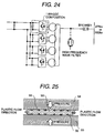
- the reason can be estimated that, when a pressure is added to a soft metallic sheet in a thickness direction to cause a plastic deformation in a lateral direction as indicated schematically in FIG. 25, deformation resistance in the lateral direction becomes extremely large, even if the soft metallic material is used, due to a friction force (friction resistance) 56 generated at the boundary between the electrode members 54, 55 interposing the soft metallic sheet 53. Even if the pressure is increased in order to cause a plastic deformation, the friction force is increased in proportion to the pressure, and the plastic deformation can not be readily caused.
- the present invention is to provide a method for ensuring an uniform press contact condition on a large area region, which has been becoming more difficult than ever in accordance with increasing the size of the package by increasing the diameter of the wafer, and with connecting multichips in parallel of the element corresponding to increasing the capacity. That is, the present invention is to provide a method, which is capable of accommodating the variation in height of the contacting plane (warps, waviness, variation in dimensions of the members, and the like), and of decreasing the thermal resistance and electrical resistance at the contacting boundary planes.
- the second object of the present invention is to provided a converter preferable for a system of a large capacity by using the semiconductor device obtained by the above methods.
- a semiconductor element comprising at least a first main electrode on a first main plane, and a second main electrode on a second main plane is assembled between a pair of main electrode plates, and a metallic body having macroscopic vacancies inside is arranged between electrodes of said semiconductor element and the main electrode plate.
- a semiconductor element comprising at least a first main electrode on a first main plane, and a second main electrode on a second main plane is assembled between a pair of main electrode plates, and any one selected from at least a metallic netting, a plate manufactured to be uneven, and a porous metallic plate is arranged between electrodes of said semiconductor element and the main electrode plate.
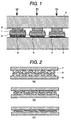
- FIG. 1 A fundamental application state of the present invention is indicated in FIG. 1.
- At least a first main electrode is formed on a first main plane, and a second main electrode is formed on a second main plane in a semiconductor element 1.
- Intermediate electrode plates 2, 3 composed of Mo, W, and the like are arranged above the both main electrode planes, and furthermore, a pair of main electrode plates (common electrode plates) 4, 5 composed of Cu, or a Cu alloy are arranged at outer side portions of the intermediate electrode plates.
- a metallic body having macroscopic vacancies inside such as a metallic netting, or a metallic plate manufactured to be uneven 6, is inserted between the intermediate electrode plate 3 and the main electrode plate 5, and all the members are contacted each other by pressing the whole together.
- FIG. 1 A fundamental application state of the present invention is indicated in FIG. 1.
- the thickness of the metallic netting, or the metallic plate manufactured to be uneven 6 which were a definite thickness before the pressing, have been decreased in the order of (a), (b), and (c) by crushing and thinning. That means, the metallic netting, or the metallic plate manufactured to be uneven, is deformed by pressing so that the total heights including the height of the metallic netting, or the metallic plate manufactured to be uneven (a sum of the heights of the members 1, 2, 3, and 6) become equal at the positions of (a), (b), and (c), and their thickness is varied.
- the semiconductor element can be mounted with ensuring a desirable press contact state at the plural chip positions (a), (b), and (c), and a semiconductor device having less variation in thermal resistance and electrical resistance can be realized.
- FIG. 1 an example wherein the metallic netting, or the metallic plated manufactured to be uneven 6 is inserted in the plane contacting with pressure facing to the main electrode plate 5 and the intermediate electrode plate 3 is indicated.
- the inserted position can be at other contacting planes such as between the main electrode plate 4 and the intermediate electrode plate 2, between the element 1 and the intermediate electrode plates 2, 3, and plural contacting planes can be used concurrently.
- the metallic netting different each other, or the metallic plates manufactured to be uneven different each other per each of the planes between the electrodes can be arranged.
- FIG. 2 is a set of schematic illustrations indicating a model of deformation processes of the metallic netting 9 provided between the electrode plate 7 and the electrode plate 8 caused by pressing.
- FIG. 2 (a) indicates a contacting state before causing a large pressure deformation, (b) indicates a state during deformation under pressing, and (c) indicates a state after the deformation is completed thoroughly by the applies pressure.
- FIG. 3 indicates the effects of the pressure on the amount of deformation in the thickness direction of the metallic netting, that is a variation in thickness, or electrical resistance when the metallic netting is contacted between two electrodes with pressure.
- the metallic netting referred to in the present invention includes, in addition to a sheet of netting woven with metallic fiber by various weaving manner, a sheet of netting woven with conductive fiber such as carbon fiber and the like, and a sheet material having a complex structure composed of an organic resin of core and a metal of surface layer.
- the material for the metallic fiber can be selected from the group consisting of soft metals having a small electrical resistance and thermal resistance such as copper, aluminum, silver, gold, and the like; significantly soft metal such as soldering material and the like; materials of inexpensive and superior in oxidation resistance such as nickel, stainless steel (SUS), and the like; and materials superior in high temperature characteristics as Ni base alloys and the like such as inconel and the like; and the material having the most suitable characteristics in consideration of the applied target can be selected.
- soft metals having a small electrical resistance and thermal resistance such as copper, aluminum, silver, gold, and the like
- significantly soft metal such as soldering material and the like
- materials of inexpensive and superior in oxidation resistance such as nickel, stainless steel (SUS), and the like
- materials superior in high temperature characteristics such as Ni base alloys and the like such as inconel and the like
- the material having the most suitable characteristics in consideration of the applied target can be selected.
- the amount of deformation can be increased if the diameter of the fiber is increased.
- the amount of deformation can be increased if the diameter of the fiber is increased.
- it is generally effective to decrease the mesh size for increasing the number of contacting points of the netting with the electrodes. Since the amount of deformation of the complex sheet material, wherein resin fiber is coated with metal, can be made larger than that of the sheet material made of metallic fiber, it is particularly effective in use, which requires a large amount of elastic deformation.
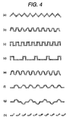
- the metallic plate manufactured to be uneven referred to in the present invention means a metallic body, which is manufactured so as to have different thickness depending on positions, in contrast with conventional metallic plate, metallic foil, and metallic sheet, which generally mean a flat dense body having substantially an uniform thickness.
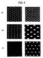
- Metallic plates called by various names such as expanded metal, meshed metal, grid metal, slit metal, punched metal, embossing manufactured plate, dimple manufactured plate, wave plate, and the like are included in the metallic plates of the present invention. Representative examples of shapes are indicated in FIG. 4 as the cross sectional shapes of the models, and examples of appearance photographs are indicated in FIG. 5 ((a) expanded metal, (b) slit manufactured plate, and (c) embossing manufactured plate).
- FIG. 6 (a) indicates a contacting state before causing a significant deformation by pressure, (b) indicates a state during deformation, and (c) indicates a state after deformation has been occurred sufficiently by pressure.
- the wave plate 10 provided between the electrode plate 7 and the electrode plate 8 is significantly deformed in a certain range of pressure, which is determined by the plate thickness, material of the plate, manufactured waving pitch, manufactured shape, and others. That means, the waving shape portion which has been manufactured to be uneven is deformed significantly by compressing, and thickness of the wave plate 10 is decreased.
- the electrodes 7, 8 come to contact with the wave plate 10 by a remarkably large area, and the pressure per area is not increased so much even if the applied load is increased. Furthermore, the variation rate of the amount of deformation becomes small, because the deformation resistance is increased as same as the case shown in FIG. 25.
- the material having the most suitable characteristics corresponding to the applied target can be selected from the group consisting of copper, aluminum, silver, gold, soldering material, nickel, stainless steel (SUS), and various alloys such as Ni base alloys and the like as same as the previous case.
- the most suitable conditions corresponding to the amount of deformation, electrical resistance, and thermal resistance required for the necessary pressure range can be selected.
- the most suitable material and surface processing are desirably selected depending on the using condition of the semiconductor device based on which must be prior to whether decreasing the thermal resistance and electrical resistance, or improving the deformation capability.
- any of a method of arranging the metallic netting, or the metallic plates manufactured to be uneven into plural different positions between electrodes, and a method of arranging a combined assembly of plural metallic netting, or plural metallic plates manufactured to be uneven into an interval between electrodes is desirable.
- a pre-treatment to assemble them into a body previously is effective.
- a method for decreasing the contacting resistance between the metallic netting, or the metallic plate manufactured to be uneven with electrodes interposing them forming a metallic layer, which is softer and more oxidation resistant than the metallic material of the metallic netting and the metallic plate, onto the surface of the metallic netting or the metallic plate by means such as printing, plating, and the like is desirable.
- a hard metallic material, or a readily oxidized metal is used.
- a Ni netting or a Ni plate manufactured to be uneven coated with a soft film made of Ag or Au, or a metallic netting or a metallic plate manufactured to be uneven made of Cu or Al having an oxidation preventing film made of Ag or Au at its surface is used.
- a method of arranging a dense metallic foil onto the surface of the metallic netting, or the metallic plate manufactured to be uneven, and forming a body together can be used.
- using a metallic foil which is softer and more oxidation resistant than the metallic material of the metallic netting and the metallic plate is effective.
- a metallic netting or a metallic plate manufactured to be uneven made of Cu or Al having a metallic foil made of any of Cu, Al, Ag, Au, and the like on its surface is used.
- a metallic netting or a metallic plate manufactured to be uneven but also a soft metallic foil can be arranged concurrently between the electrodes.
- a method for ensuring approximately same amount of deformation with the same loading even if the contacting areas differ each other by inserting an Au foil between the upper main electrode plate and the intermediate electrode plate, and inserting a metallic netting or a metallic plate manufactured to be uneven between the lower main electrode plate and the intermediate electrode plate is effective.
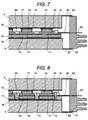
- FIG. 7 indicates an embodiment of the present invention applied to a reverse conductive type switching device, wherein a flywheel diode(FWD) 12 connected to a switching device using IGBT 11 in reverse parallel is integrated.
- FIG. 7 indicates a partial cross section from outer most portion of the press contact type semiconductor device at right side to the middle portion toward the center.
- an emitter electrode is formed on almost whole plane of a first main plane at upper side
- a collector electrode is formed on a second main plane at lower side
- an electrode for controlling (gate electrode) is formed on the first main plane.
- an anode electrode is formed on the upper plane of the silicon substrate, and a cathode electrode is formed on the lower plane of the silicon substrate.
- Each of these semiconductor chips is arranged on an integrated intermediate electrode 14 made of Mo, which operates to remove heat and concurrently to connect electrically, and, furthermore, is arranged so as to contact with each of the main electrodes on the chips via each intermediate electrode 13 per respective of the chips.
- This composition is further interposed between a first common main electrode plate (Cu) 4 and a second common main electrode plate (Cu) 5.
- a wave plate 17 made of Cu, i.e. a metallic plate manufactured to be uneven, is inserted between the intermediate electrode 13 and the common main electrode plate 4.
- An Au plated film 15 is formed on the surface of the intermediate electrode plate by approximately 1 ⁇ m in thickness, and a Ni plated film 16 is formed on the surface of the common electrode plate by approximately 1-3 ⁇ m in thickness.
- the above semiconductor chips and the intermediate electrode are fixed mutually by a frame 24.
- a lead wire is taken out from the gate electrode 18 of the IGBT chip 11 by a wire bond 19, and is connected to the gate electrode wiring plate 20 formed on the intermediate electrode 14.
- An interval between the above pair of common main electrode plate 4, 5 is insulated externally by an insulating outer cylinder 21 made of ceramics and the like, and a hermetic structure is formed at an interval between the common main electrode plate and the insulating outer cylinder by sealing inside the package by a metallic plate 22.
- the gate electrode lead is taken out to outside the package by a sealed wiring 23 through the external cylinder 21.
- the above wave plate 17 used in the present embodiment was made of Cu, its wave pitch was 1 mm, the thickness of the plate was 0.3 mm, and its surface was thin gold plated. The whole thickness of the wave plate including the initial uneven portion was 0.6 mm. Variation in thickness of the intermediate electrode plate mounted practically in the present embodiment was 100 ⁇ m at maximum. However, results of determining pressure distribution by inserting pressure sensitive paper between the intermediate electrode plate 14 and the chips 11, 12 revealed that the pressure difference was small, and they were pressed almost uniformly.
- FIG. 8 indicates an embodiment of the present invention applied to a reverse conductive type switching device, wherein a MOS control type switching device 11 and a flywheel diode 12 are integrated.
- Main electrodes (collector, cathode) at lower side of each of these semiconductor chips are made of Au, and are connected to an intermediate electrode 14, whereon an Ag plated film 15 of 2-3 ⁇ m thick is formed previously, by heating and pressure welding.
- main electrodes (emitter, anode) at upper side of each of these semiconductor chips are made of Al, and are connected to an intermediate electrode 13, whereon an Au plated film 15 of 1-2 ⁇ m thick is formed previously.
- the above integrated intermediate bodies of electrodes and semiconductor chips are arranged in parallel between a first common main electrode plate (Cu) 4, a Ni plated film 16 of 2-4 ⁇ m thick is formed on its surface previously, and a second common main electrode plate (Cu) 5.
- a second common main electrode plate (Cu) 5 In this case, an expanded metal plate 17 was inserted as the metallic plate manufactured to be uneven between the intermediate electrode 14 and the common main electrode plate 5, and the whole body was pressed via both of the common main electrode plates 4, 5.
- the expanded metal plate 17 was made of Ag, thickness of the metal plate was approximately 0.1 mm, approximately 3000 mesh, and the whole thickness including the initial uneven portion was approximately 0.25 mm. Variation in thickness at each position of the chips mounted practically in the present embodiment was 80 ⁇ m at maximum. However, results of determining pressure distribution by inserting pressure sensitive paper between the intermediate electrode plate 13 and the common main electrode plate 4 revealed that the pressure difference was small, and they were pressed almost uniformly.
- FIG. 9 indicates an example of mounting state, wherein a pin 25 for taking out a gate control electrode from the chip is formed at the center of the chip.
- FIG. 9 indicated an embodiment of the present invention applied to a reverse conductive type switching device, wherein a flywheel diode (FWD) 12 connected to a switching device using IGBT 11 in reverse parallel was integrated, as same as shown in FIG. 7.
- Main electrodes (collector, cathode) at lower side of each of these semiconductor chips are made of Au, and are connected to an intermediate electrode 14, whereon an Ag plated film of 2-3 ⁇ m thick is formed previously, by heating and pressure welding.
- the surface of the intermediate electrode 13 is plated with an Au film 15 of 2-3 ⁇ m thick, and is connected to each of the semiconductor chips by press contact.
- the above integrated bodies of electrodes and semiconductor chips are inserted between a first common main electrode plate (Cu) 4 and a second common main electrode plate (Cu) 5.
- complex metallic netting 17 composed of double-overlapped netting manufactured in a shape having a hole at the center are arranged around the pin 25 and a member 26 for insulating the pin between the intermediate electrode plate 13 and the common electrode plate 4. In accordance with this method, shifting the location of respective complex netting 17 can be prevented by the member 26 for insulating the central pin, and an assembling operation can be performed easily.
- the complex netting composed of double-overlapped metallic netting can be integrated to a body at their peripheral portion by stamping the double-overlapped netting to a designated shape using a die, and the complex netting can be handled as a single complex netting component.
- the gate circuit 27 is contained in a groove 28 provided to the first common main electrode plate (Cu), taken out to the periphery of the package, and further taken out by the wire 29, 23 to outside the package.
- the complex netting made of Cu was used, and its surface was plated with Au in order to decrease the contacting resistance, further. Accordingly, the contacting resistance between the intermediate electrode plate and the common electrode plate could be decreased significantly. The above effect was remarkable in the region where the pressure was small. Variation in thickness at each position of the chips mounted practically in the present embodiment was 200 ⁇ m at maximum. However, results of determining pressure distribution by inserting pressure sensitive paper between the intermediate electrode plate 14 and the common main electrode plate 5 revealed that the pressure difference was small, and they were pressed almost uniformly.
- FIG. 10 indicates an embodiment of the present invention applied to a GTO.
- a semiconductor element substrate 31 is made of silicon (Si), and has at least a PN junction inside.
- Cathode electrodes and gate electrodes made of aluminum (Al) are formed on one of main planes of the semiconductor element substrate 31, and anode electrodes made of aluminum (Al) are formed on another main plane.
- Intermediate electrode plates 32, 33 made of molybdenum (Mo) are arranged on the upper side of the cathode electrode and the anode electrode, respectively.
- Metallic netting 34, 35 made of Cu were arranged between the intermediate electrode plates 32, 33 and a pair of external main electrode plates 4, 5 made of copper (Cu), and the whole body was pressed.
- a cap member 36 is arranged at side planes of the semiconductor element substrate 31.
- a part of gate lead 37 is arranged and contacted on the gate electrode on the semiconductor substrate, and the part is contacted with the gate electrode by pressing with the gate insulator 38 and a disc spring 39. All the above parts are arranged in a sealed package surrounded by an insulator 40, a pair of external electrodes 4, 5, and a flange 41. Another end of the gate lead 37 is taken out outside the insulator 40 via a sealing structure as a gate terminal.
- FIG. 11 indicates an embodiment, wherein a punching metal 42 made of Cu, a dense Ag thin film layer is formed on its surface, is arranged between a cathode electrode side of a semiconductor element 31 of wafer size and an intermediate electrode plate 32.
- the variation in height could be absorbed with the punching copper plate 42 better than a flat copper plate, and contacting resistance could be decreased.
- FIG. 12 indicates an embodiment, wherein no intermediate electrode plate is inserted between a collector side electrode of the semiconductor chip 1 and a main electrode plate 5.
- a metallic netting, or a metallic plate manufactured to be uneven was arranged between an intermediate electrode plate 2 and a main electrode plate 4 of emitter side.
- an embossed plate 44 manufactured to have slits was used as the metallic plate manufactured to be uneven.
- a soft metal foil 45 was inserted between a chip main electrode and a main electrode plate 5, in order to decrease further contacting resistance and to protect the chips.
- the material for the intermediate electrode a material having a thermal expansion coefficient at a middle of Si and a material of the external main electrode, and a desirable thermal conductivity and electrical conductivity is used.
- a single metal such as tungsten (W), molybdenum (Mo), or complex material or alloys containing these element as a main composition material such as Cu-W, Ag-W, Cu-Mo, Ag-Mo, Cu-FeNi, and the like
- a complex material of metal with ceramics or carbon for instance, such as Cu/SiC, Cu/C, Al/SiC, Al/AlN, Cu/Cu 2 O, and the like are desirable.
- a conductive material having a desirable thermal conductivity such as copper, aluminum, and their alloys, for instance, using Cu-Ag, Cu-Sn, Cu-Zr, Cu-Zr-Cr, Cu-Ni-Si-Zr, and the like, or the above complex materials are desirable.
- FIG. 13 indicates another applying state of the present invention. At least a first main electrode is formed on a first main plane of a semiconductor element 1, and a second main electrode is formed on a second main plane. Intermediate electrode plates 2, 3 made of Mo, or W and others are arranged on both of the main electrode planes, and furthermore, common electrode plates (main electrode plate) 4, 5 made of a pair of copper, and the like, are arranged at outer portions of the intermediate electrode plates. A porous metallic plate 6, as an example of metallic body having macroscopic vacancies inside, is inserted between the intermediate electrode plate 3 and the main electrode late 5, and each of the members are contacted by pressing its whole body together. FIG.
- the thickness of the porous metallic plates 6 are decreased in the order of (a), (b), and (c) after contacting with pressure, although their thickness before contacting have been same. That means, the thickness of the porous metallic plate has been varied so as to make the whole height including the height of the porous metallic plate (a sum of the members 1, 2, 3, and 6) equal at the positions of (a), (b), and (c).
- the inserting position can be varied to other contacting planes, such as between the main electrode plate 4 and the intermediate electrode plate 2, between the element 1 and the intermediate electrode plates 2, 3, and plural boundary planes can be used concurrently.
- various porous metallic plates made of different material each other can be arranged at respective of intervals between the electrodes.
- the porous metal referred to in the present invention is metallic material including a large number of voids, while terminology of metallic plate, metallic foil, and metallic sheet mean in general substantially dense metallic members.
- the porous metal has a fine structure, wherein three dimensional random network of continuous metallic portions is formed.
- Examples of the porous metal include foamed metal, sponge metal, porous metal, foam metal, and the like.
- the soft materials having a small electrical resistance and thermal resistance such as copper, aluminum, silver, gold, and the like, and materials of inexpensive and superior in oxidation resistance such as nickel, stainless steel (SUS), and the like are preferable in particular, and the material having the most suitable characteristics in consideration of the applied target can be selected.
- FIG. 14 indicates the effects of the pressure on the amount of deformation (the amount of change in the thickness of porous metallic plate) and electrical resistance, determined by using a porous Cu plate (foamed metal copper plate) as the representative of the porous metallic plate.
- a porous Cu plate Foamed metal copper plate
- the foamed metal copper plate is prepared by the steps of; forming a coated film of copper powder on surface of vacancies in foamed urethane by dry adhesion method; removing the urethane by thermal processing; and sintering the copper powder in a reducing atmosphere.
- the foamed metal copper plate is a porous copper metal plate having a three dimensional network skeleton of copper.
- Another method wherein Cu coating film is formed on surface of foamed resin by a wet plating method, is similarly usable. Thickness of the porous Cu plate is decreased accompanied with increasing pressure. The porous Cu plate is deformed significantly in a specific pressure region (approximately 0.5 - 2 kg/mm 2 ), and the amount of deformation is decreased accompanied with increasing its density. The electrical resistance is decreased with increasing the pressure, and is changed significantly in the specific region of remarkable deformation of the porous Cu plate. On the contrary, in case of Cu thin plate, significant deformation caused by plastic deformation is not generated even if a pressure exceeding its yield stress is applies as explained previously (FIG. 25), but only minor deformation as much as elastic deformation is generated. Electrical resistance is decreased gradually, because contact resistance with measuring electrode is decreased in accordance with increasing pressure.
- the porous metal different from the case of dense metal foil (thin plate) (FIG. 25), a large deformation can be occurred by relatively small pressure, because the porous metal itself has vacancies at its interior portion, and microscopically the material pressed with a force can be moved easily to these vacancies.
- the deformation is occurred substantially only in a thickness direction (a pressing direction), because the porous metal itself has vacancies, which make it possible to absorb the deformation, at its interior portion, and deformation resistance by friction in a lateral direction at the contacting planes. Accordingly, the porous metal after the deformation has less vacancies than the initial period, and becomes dense.
- the shape of the vacancy is varied to be flatten in the thickness direction.
- the material of the present invention makes it possible to decrease electrical resistance and thermal resistance effectively with ensuring an capability to cause significant deformation to the thickness direction, because the material of the present invention has a feature that metallic channel portion particularly in the thickness direction is more increased by deformation with pressure in comparison with the lateral direction.
- conventional dense material is deformed (decreasing its thickness) significantly, the material as much as its changed volume flows plastically in the lateral direction, and a phenomenon that side plane of the material is swelled remarkably can be observed.
- the porous material when used, its side plane is scarcely swelled even if it is deformed (decreasing its thickness) significantly, because the porous metal itself has sufficient vacancies, which makes it possible to absorb the deformation of the material, at its interior portion. Therefore, since any problems such as contacting with adjacent material are not generated, the porous material is suitable for high density mounting.
- a large fraction of vacancy in the porous metallic material before the deformation is desirable, larger than 50 % is desirable, and particularly a range of 60-80 % is preferable.
- the contacting resistance (electricity, heat) in the practical using condition at a boundary with the electrodes interposing the porous metallic plate becomes an important factor.
- a microscopic shape at the outermost surface of the porous metallic plate is more desirable to be a structure shown in FIG. 15 (b), which has a large number of terminal parts in approximately parallel to the contacting surface, or of terminal parts 8 having a large declining angle as possible, than a structure shown in FIG. 15 (a), which has a large number of columnar metal 7 extruding perpendicularly to the contacting surface.
- FIG. 16 and FIG. 17 indicate an embodiment, wherein a metallic layer 9, which is softer and more oxidation resistant than the metallic material of the porous metallic plate, is formed onto the surface of the porous metallic plate 6 by means such as printing, plating, and the like.
- FIG. 17 (a) indicates an embodiment, wherein a dense metallic foil 10 is arranged onto the surface of porous metallic plate 6 and a body is formed together.
- a metallic foil which is softer and more oxidation resistant than the metallic material of the porous metallic plate, in addition to the same material as the porous metallic material, is effective.
- a porous metallic plate made of Cu or Al having a metallic foil made of any of Cu, Al, Ag, Au, and the like on its surface is used.
- FIG. 17 (b) indicates a cross section of a plate obtained by punching out from the material indicated in FIG. 17 (a) with a pressing machine. Because the end planes are crushed when pressing is performed, the porous metallic plate becomes a shape that side planes are also covered with the surface foil. Therefore, the above method is simple and convenient method for a case when side planes of the porous metallic plate are desirably protected with a dense film. As further another method, a method for increasing its density only at the surface of the porous metallic plate by exposing it to a high temperature for a short time can be used.
- FIG. 18 indicates an embodiment of the present invention applied to a reverse conductive type switching device, wherein a flywheel diode (FWD) 12 connected to a switching device using IGBT 11 in reverse parallel is integrated.
- FIG. 18 indicates a partial cross section from outermost portion of the press contact type semiconductor device at right side to the middle portion toward the center.
- an emitter electrode is formed on almost whole plane of a first main plane at upper side
- a collector electrode is formed on a second main plane at lower side
- an electrode for controlling (gate electrode) is formed on the first main plane.
- an anode electrode is formed on the upper plane of the silicon substrate, and a cathode electrode is formed on the lower plane of the silicon substrate.
- Each of these semiconductor chips is arranged on an integrated intermediate electrode 14 made of Mo, which operates to remove heat and concurrently to connect electrically, and, furthermore, is arranged so as to contact with each of the main electrodes on the chips via each intermediate electrode 13 per respective of the chips.
- This composition is further interposed between a first common main electrode plate (Cu) 4 and a second common main electrode plate (Cu) 5.
- a porous copper plate 17 is inserted between the intermediate electrode 13 and the common main electrode plate 4.
- An Au plated film 15 is formed on the surface of the intermediate electrode by approximately 3-5 ⁇ m in thickness, and a Ni plated film 16 is formed on the surface of the common electrode plate by approximately 1-3 ⁇ m in thickness.
- the above semiconductor chips and the intermediate electrode are fixed mutually by a frame 24 made of teflon .
- a lead wire is taken out from the gate electrode 18 of the IGBT chip 11 by a wire bond 19, and is connected to the gate electrode wiring plate 20 formed on the intermediate electrode 14 .
- An interval between the above pair of common main electrode plates 4, 5 is insulated externally by an insulating outer cylinder 21 made of ceramics and the like, and a hermetic structure is formed at an interval between the common main electrode plate and the insulating outer cylinder by sealing inside the package by a metallic plate 22.
- the gate electrode lead is taken out to outside the package by a sealed wiring 23 through the external cylinder 21.
- the above porous copper plate was prepared by the steps of; forming a sheet from Cu powder slurry by doctor blade method, calcining the sheet for removing organic binder components, and reducing and pre-sintering the Cu powder so as to remain voids at a higher temperature.
- Initial void fraction was 60 %
- average void diameter was 30 ⁇ m
- thickness was 150 ⁇ m.
- Variation in thickness of the intermediate electrode plate mounted practically in the present embodiment was 50 ⁇ m at maximum.
- results of determining pressure distribution by inserting pressure sensitive paper between the intermediate electrode plate 14 and the chips 11, 12 revealed that the pressure difference was small, and they were pressed almost uniformly.
- FIG. 19 indicates an embodiment of the present invention applied to a reverse conductive type switching device, wherein a MOS control type switching device 11 and a flywheel diode 12 are integrated.
- Main electrodes (collector, cathode) at lower side of each of these semiconductor chips are made of Au, and are connected to an intermediate electrode 14, whereon an Ag plated film 15 of 2-3 ⁇ m thick is formed previously, by heating and pressure welding.
- main electrodes (emitter, anode) at upper side of each of these semiconductor chips are made of Al, and are connected to an intermediate electrode 13, whereon an Au plated film 15 of 1-2 ⁇ m thick is formed previously.
- the above integrated intermediate bodies of electrodes and semiconductor chips are arranged in parallel between a first common main electrode plate (Cu) 4, an Ag plated film 16 of 2-4 ⁇ m thick is formed on its surface previously, and a second common main electrode plate (Cu) 5.
- a porous Ni plate 17 was inserted between the intermediate electrode 14 and the common main electrode late 5, and the whole body was pressed via both of the common main electrode plates 4, 5.
- the porous Ni plate 17 was obtained by the steps of; processing foamed resin for making it have conductivity, plating with electrolytic Ni, heat treating for removing the foamed resin by burning. This material was further pressed to be formed as a plate material having a void diameter of approximately 0.2 mm, the number of cells of 60 pieces/inch, thickness of the metallic channel portion of 40-80 ⁇ m, plate thickness of 0.6 mm, and void fraction of approximately 80 %.
- the contacting resistance between the porous Ni plate and the above electrodes is reduced significantly, because both of the surfaces of electrodes at both sides interposing the porous Ni plate are plated with Ag. Variation in thickness at each position of the chips mounted practically in the present embodiment was 100 ⁇ m at maximum.
- results of determining pressure distribution by inserting pressure sensitive paper between the intermediate electrode plate 13 and the common main electrode plate 4 revealed that the pressure difference was small, and they were pressed almost uniformly.
- the porous metallic plate In order to realize correction of the height and decrease of the electrical resistance and the thermal resistance at optimum, not only the porous metallic plate, but also soft metal foil can be inserted concurrently between the electrodes. For instance, a following method is effective; wherein an Au foil is inserted between the upper main electrode plate and the intermediate electrode plate, and a porous Ni plate is inserted between the lower main electrode plate and the intermediate electrode plate, for ensuring approximately same amount of deformation with a same loading even in a case when the contacting areas differ each other.
- FIG. 20 indicates an example of mounting state, wherein a pin 25 for taking out a gate control electrode from the chip is formed at the center of the chip.
- FIG. 20 indicated an embodiment of the present invention applied to a reverse conductive type switching device, wherein a flywheel diode (FWD) 12 connected to a switching device using IGBT 11 in reverse parallel was integrated, as same as shown in FIG. 18.
- Main electrodes (collector, cathode) at lower side of each of these semiconductor chips are made of Au, and are connected to an intermediate electrode 14, whereon an Ag plated film of 2-3 ⁇ m thick is formed previously, by heating and pressure welding.
- the surface of the intermediate electrode 13 is plated with an Au film 15 of 2-3 ⁇ m thick, and is connected to each of the semiconductor chips by press contact.
- the above integrated bodies of electrodes and semiconductor chips are inserted between a first common main electrode plate (Cu) 4 and a second common main electrode plate (Cu) 5, on each surface of them an Au plated film of 2-4 ⁇ m thick is formed.
- a porous copper plates 17 manufactured in a shape having a hole at the center are arranged around the pin 25 and a member 26 for insulating the pin between the intermediate electrode plate 13 and the common electrode plate 4. In accordance with this method, shifting the location of respective porous metallic plate 17 can be prevented by the member 26 for insulating the central pin, and an assembling operation can be performed readily.
- the gate circuit 27 is contained in a groove 28 provided to the first common main electrode plate (Cu) 4, taken out to the periphery of the package, and further taken out by the wire 29, 23 to outside the package.
- a complex porous copper plate was utilized as the porous metallic plate in the present embodiment.
- the complex porous copper plate has a structure as shown in FIG. 17, wherein a dense copper foil was integrated onto the surface of the porous plate. Accordingly, the contacting resistance between the porous metallic plate and the intermediate electrode plate, and the common electrode plate could be decreased significantly. The above effect was remarkable in the region where the pressure was small, and the contacting resistance could be decreased from 1/5 to 1/10.
- Variation in thickness at each position of the chips mounted practically in the present embodiment was 200 ⁇ m at maximum.
- results of determining pressure distribution by inserting pressure sensitive paper between the intermediate electrode plate 14 and the common main electrode plate 5 revealed that the pressure difference was small, and they were pressed almost uniformly.
- the intermediate electrode plates having various average thickness depending on the kinds of the chips are prepared; large difference of the thickness of the chips are adjusted with the intermediate electrode plates; furthermore, the porous metallic plate of the present invention is used for accommodating the variation in height of the intermediate electrode plates and the semiconductor chips.
- FIG. 21 indicates an embodiment, wherein a porous copper plate 30, on which surface a dense thin film layer 33 of Ag is formed as a body, is arranged between cathode electrode side of a wafer size semiconductor element 31 and an intermediate electrode plate 32.
- the porous copper plate had an average void diameter of approximately 0.1 mm, cell number of 40 pieces/mm 2 , thickness of metallic channel of 30-50 ⁇ m, plate thickness of 0.8 mm, and void fraction of approximately 75 %.
- variation of height is absorbed, and the contacting resistance can be decreased by compensating the decrease in contacting area based on voids at the surface of the porous metal.
- FIG. 22 indicates an embodiment, wherein no intermediate electrode plate is inserted between a collector side electrode of the semiconductor chip 1 and a common electrode plate.
- a porous metallic plate was arranged between the common electrode plate 5 and the semiconductor element 1
- the porous metallic plate 36 is arranged in a region same or smaller than the shape of the intermediate electrode plate 2, on which surface a soft metal film 38 is formed.
- a soft metal foil 37 is inserted between a chip main electrode and the porous metallic plate, in order to decrease further contacting resistance and to protect the chips.
- metals mainly such as Cu, Al, Ag, Au, Ni, and the like, or their alloy are desirable. Based on using state of the semiconductor device, it is desirable to select optimum material and surface treatment in consideration of priority of decreasing the thermal resistance and electrical resistance, and improving deformation capability.
- the material for the intermediate electrode a material having a thermal expansion coefficient at a middle of Si and a material of the external main electrode, and a desirable thermal conductivity and electrical conductive is used.
- a single metal such as tungsten (W), molybdenum (Mo), or complex material or alloys containing these element as a main composition material such as Cu-W, Ag-W, Cu-Mo, Ag-Mo, Cu-FeNi, and the like, a complex material of metal with ceramics or carbon, for instance, such as Cu/SiC, Cu/C, Al/SiC, Al/AlN, and the like are desirable.
- a conductive material having a desirable thermal conductivity such as copper, aluminum, and their alloys, or the above complex materials are desirable.
- the mounting method of the present invention can be applied naturally to the press contact type semiconductor devices composed of no diode, but only switching semiconductors such as IGBT and the like. Additionally, the mounting method of the present invention is naturally effective in mounting, for instance, a large number of diodes in a press contact type package by the above method. Furthermore, the above embodiments are explained using mainly IGBT, but targets of the present invention are all the semiconductor elements comprising at least a first main electrode on a first main plane and a second main electrode on a second main plane.
- the present invention can be applied to the insulated gate type transistors (MOS transistor) other than the IGBT, the insulated gate type thyristors (MOS controlled thyristor) including IGCT (Insulated Gate Controlled Thyristor) , GTO, thyristors, and diodes, and others in a similar way. Furthermore, the present invention is effective to the compound semiconductor elements such as SiC other than Si element, GaN, and the like.
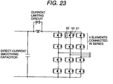
- the IGBT elements 40 as the main converting elements and diode elements 41 are arranged in reverse parallel, and the converter is composed by connecting n pieces of these elements in series.
- IGBT and diodes indicate the press contact type semiconductor device, wherein a large number of semiconductor chips are mounted in parallel, by the present invention.
- the IGBT chips and the diode chips in the figures are assembled and contained in a package.
- snubber circuits 42 and a current limiting circuit are added to the above assembly.
- a composition of self-commutated converter using four bridges of the three phase bridge indicated in FIG. 23 is indicated in FIG. 24.
- the press contact type semiconductor devices of the present invention are mounted in a shape called a stack structure, wherein a plurality of the semiconductor devices connected in series interposing water-cooled electrodes in a shape to contact with outer side plane of the main electrode plate, and the whole stack is pressed together.
- uniform contact can be obtained with lower pressure than conventional products. Therefore, an effect to simplify the above stack structure and the like can be realized.
- the press contact type semiconductor device of the present invention is particularly preferable not only for the above embodiments, but also for self-commutated large capacity converters using for power systems, and for large capacity converter using for mill. Furthermore, the press contact type semiconductor device of the present invention can be used for variable speed pumped storage power plant, substation facilities in building, substation facilities for railway, sodium-sulfur (NaS) battery systems, and converter for traction and the like.
- NaS sodium-sulfur
- uniform press contact state in a large area region which has been becoming more difficult with increasing the size of package accompanied with increasing the diameter of wafer and increasing the number of chips connected in parallel in an element corresponding to increasing the capacity, can be easily realized with a relatively low pressure. That is, the variation in height of the contacting plane can be absorbed sufficiently, and thermal resistance and electrical resistance at contacting boundary planes can be decreased.
Applications Claiming Priority (6)
| Application Number | Priority Date | Filing Date | Title |
|---|---|---|---|
| JP1011898 | 1998-01-22 | ||
| JP1011898 | 1998-01-22 | ||
| JP10434498 | 1998-04-15 | ||
| JP10434498A JP3617306B2 (ja) | 1998-04-15 | 1998-04-15 | 加圧接触型半導体装置、及びこれを用いた変換器 |
| JP22784798A JP3721795B2 (ja) | 1998-01-22 | 1998-08-12 | 圧接型半導体装置、及びこれを用いた変換器 |
| JP22784798 | 1998-08-12 |
Publications (2)
| Publication Number | Publication Date |
|---|---|
| EP0932201A2 true EP0932201A2 (de) | 1999-07-28 |
| EP0932201A3 EP0932201A3 (de) | 2000-03-22 |
Family
ID=27278843
Family Applications (1)
| Application Number | Title | Priority Date | Filing Date |
|---|---|---|---|
| EP99100944A Withdrawn EP0932201A3 (de) | 1998-01-22 | 1999-01-20 | Halbleiteranordnung vom Druckkontakttyp und Umformer der diese anwendet |
Country Status (5)
| Country | Link |
|---|---|
| US (2) | US6495924B2 (de) |
| EP (1) | EP0932201A3 (de) |
| KR (1) | KR19990067924A (de) |
| CN (1) | CN1236982A (de) |
| CA (1) | CA2259846A1 (de) |
Cited By (10)
| Publication number | Priority date | Publication date | Assignee | Title |
|---|---|---|---|---|
| DE10048436A1 (de) * | 2000-09-29 | 2002-04-18 | Siemens Ag | Elektronische Leistungsschaltervorrichtung |
| DE10048859A1 (de) * | 2000-10-02 | 2002-04-18 | Infineon Technologies Ag | Druckkontaktanordnung sowie deren Verwendung |
| EP1389802A1 (de) * | 2002-08-16 | 2004-02-18 | ABB Schweiz AG | Schutzschicht für Leistungshalbleitermodul-Kontaktplättchen |
| EP2257142A1 (de) * | 2009-05-26 | 2010-12-01 | Semikron Elektronik GmbH & Co. KG Patentabteilung | Befestigung eines Bauelementes an einem Substrat und/oder eines Anschlusselementes an dem Bauelement oder an dem Substrat durch Drucksinterung |
| CN103380495A (zh) * | 2012-01-11 | 2013-10-30 | 松下电器产业株式会社 | 压接型半导体装置及其制造方法 |
| US20140353818A1 (en) * | 2013-06-04 | 2014-12-04 | Infineon Technologies Ag | Power module comprising two substrates and method of manufacturing the same |
| DE102013219433A1 (de) * | 2013-09-26 | 2015-03-26 | Siemens Aktiengesellschaft | Elektronisches Leistungsmodul mit elastischen Kontakten und Stapelaufbau mit einem solchen Leistungsmodul |
| WO2016000762A1 (de) * | 2014-07-01 | 2016-01-07 | Siemens Aktiengesellschaft | Spannverband mit druckstück |
| EP3306663A1 (de) * | 2016-10-05 | 2018-04-11 | ABB Schweiz AG | Sic-auf-si-basiertes halbleitermodul mit kurzschlussfehlermodus |
| WO2021052758A1 (en) * | 2019-09-17 | 2021-03-25 | Danfoss Silicon Power Gmbh | Method of forming a cohesive connection between a semiconductor with an aluminium coated contact surface and a shaped metal body, as well as a semiconductor module comprising and a shaped metal body cohesively attached to a semiconductor |
Families Citing this family (50)
| Publication number | Priority date | Publication date | Assignee | Title |
|---|---|---|---|---|
| JP2001210761A (ja) * | 2000-01-24 | 2001-08-03 | Shinko Electric Ind Co Ltd | 半導体装置及びその製造方法 |
| EP2244289B1 (de) * | 2000-04-19 | 2014-03-26 | Denso Corporation | Kühlmittelgekühltes Halbleiterbauelement |
| US6887769B2 (en) * | 2002-02-06 | 2005-05-03 | Intel Corporation | Dielectric recess for wafer-to-wafer and die-to-die metal bonding and method of fabricating the same |
| US6661085B2 (en) * | 2002-02-06 | 2003-12-09 | Intel Corporation | Barrier structure against corrosion and contamination in three-dimensional (3-D) wafer-to-wafer vertical stack |
| US6975016B2 (en) * | 2002-02-06 | 2005-12-13 | Intel Corporation | Wafer bonding using a flexible bladder press and thinned wafers for three-dimensional (3D) wafer-to-wafer vertical stack integration, and application thereof |
| US6762076B2 (en) * | 2002-02-20 | 2004-07-13 | Intel Corporation | Process of vertically stacking multiple wafers supporting different active integrated circuit (IC) devices |
| JP2004023083A (ja) * | 2002-06-20 | 2004-01-22 | Toshiba Corp | 圧接型半導体装置 |
| US6987032B1 (en) | 2002-07-19 | 2006-01-17 | Asat Ltd. | Ball grid array package and process for manufacturing same |
| US6800948B1 (en) * | 2002-07-19 | 2004-10-05 | Asat Ltd. | Ball grid array package |
| US6979594B1 (en) | 2002-07-19 | 2005-12-27 | Asat Ltd. | Process for manufacturing ball grid array package |
| JP4210908B2 (ja) * | 2003-02-19 | 2009-01-21 | 株式会社デンソー | 半導体モジュール |
| US7193326B2 (en) * | 2003-06-23 | 2007-03-20 | Denso Corporation | Mold type semiconductor device |
| US7372151B1 (en) | 2003-09-12 | 2008-05-13 | Asat Ltd. | Ball grid array package and process for manufacturing same |
| US7397968B2 (en) * | 2003-10-29 | 2008-07-08 | Hewlett-Packard Development Company, L.P. | System and method for tone composition |
| JP2005251784A (ja) * | 2004-03-01 | 2005-09-15 | Renesas Technology Corp | 半導体モジュールおよびその製造方法 |
| US7091581B1 (en) | 2004-06-14 | 2006-08-15 | Asat Limited | Integrated circuit package and process for fabricating the same |
| US7411289B1 (en) | 2004-06-14 | 2008-08-12 | Asat Ltd. | Integrated circuit package with partially exposed contact pads and process for fabricating the same |
| US7087538B2 (en) * | 2004-08-16 | 2006-08-08 | Intel Corporation | Method to fill the gap between coupled wafers |
| US8610262B1 (en) | 2005-02-18 | 2013-12-17 | Utac Hong Kong Limited | Ball grid array package with improved thermal characteristics |
| US7593228B2 (en) * | 2005-10-26 | 2009-09-22 | Indium Corporation Of America | Technique for forming a thermally conductive interface with patterned metal foil |
| JP4764159B2 (ja) * | 2005-12-20 | 2011-08-31 | 富士通セミコンダクター株式会社 | 半導体装置 |
| JP5253161B2 (ja) | 2006-06-07 | 2013-07-31 | 三菱電機株式会社 | 熱抵抗体ならびにこれを用いた半導体装置および電気装置 |
| EP2088623A1 (de) * | 2008-02-07 | 2009-08-12 | ABB Oy | Elektrisches Modul mit mehreren elektrischen Bauelementen |
| US20110212379A1 (en) * | 2008-11-21 | 2011-09-01 | Jean Yamanis | Method of forming a fuel cell sheet |
| US8531027B2 (en) * | 2010-04-30 | 2013-09-10 | General Electric Company | Press-pack module with power overlay interconnection |
| US8368208B2 (en) * | 2010-10-01 | 2013-02-05 | Raytheon Company | Semiconductor cooling apparatus |
| WO2012172991A1 (ja) * | 2011-06-16 | 2012-12-20 | 富士電機株式会社 | 半導体ユニットおよびそれを用いた半導体装置 |
| EP2544229A1 (de) * | 2011-07-07 | 2013-01-09 | ABB Research Ltd. | Leistungshalbleiteranordnung |
| JP5529208B2 (ja) * | 2011-08-25 | 2014-06-25 | トヨタ自動車株式会社 | パワーモジュールの構造及び成形方法 |
| KR101252014B1 (ko) | 2011-11-22 | 2013-04-08 | 주식회사 브이씨텍 | 대전류용 병렬 스위치 배열을 갖는 인버터 |
| JP6094592B2 (ja) | 2012-10-01 | 2017-03-15 | 富士電機株式会社 | 半導体装置とその製造方法 |
| CN102915985B (zh) * | 2012-10-09 | 2015-06-03 | 天津大学 | 一种功率电子器件双面粘接结构及制备方法 |
| CN104183556B (zh) * | 2013-05-23 | 2018-09-14 | 国家电网公司 | 一种全压接式绝缘栅双极晶体管器件 |
| US9177943B2 (en) | 2013-10-15 | 2015-11-03 | Ixys Corporation | Power device cassette with auxiliary emitter contact |
| US9941229B2 (en) * | 2013-10-31 | 2018-04-10 | Infineon Technologies Ag | Device including semiconductor chips and method for producing such device |
| DE102014102493A1 (de) * | 2014-02-26 | 2015-08-27 | Infineon Technologies Bipolar Gmbh & Co. Kg | Verbesserte Scheibenzelle für mehrere druckkontaktierte Halbleiterbauelemente |
| CN104979224B (zh) * | 2014-04-04 | 2017-10-20 | 中国科学院苏州纳米技术与纳米仿生研究所 | 一种器件封装互联方法 |
| CN104779228B (zh) * | 2015-04-14 | 2018-09-28 | 天津大学 | 一种功率半导体模块三维封装的结构和方法 |
| CN107230644B (zh) * | 2016-03-25 | 2020-06-12 | 胡迪群 | 具有金属海绵的金属柱 |
| DE102017203132A1 (de) | 2017-02-06 | 2018-08-09 | Siemens Aktiengesellschaft | Leistungsmodul |
| CN107706299B (zh) * | 2017-08-22 | 2020-04-10 | 长安大学 | 一种适用于道路压电发电的堆叠式压电换能器及制作方法 |
| CN109827693B (zh) * | 2019-03-22 | 2023-09-12 | 华北电力大学 | 一种压接型功率半导体器件内部压力分布测量系统 |
| DE102019111964A1 (de) * | 2019-05-08 | 2020-11-12 | Danfoss Silicon Power Gmbh | Halbleitermodul mit einem ersten Substrat, einem zweiten Substrat und einen Abstandhalter, der die Substrate voneinander trennt |
| CN110416187B (zh) * | 2019-06-28 | 2021-07-09 | 西安中车永电电气有限公司 | 一种新型压接式igbt内部封装结构 |
| DE102019211084A1 (de) * | 2019-07-25 | 2021-01-28 | Siemens Aktiengesellschaft | Leistungsmodul und Verfahren zur Herstellung eines Leistungsmoduls |
| JP7395452B2 (ja) * | 2020-09-23 | 2023-12-11 | 株式会社東芝 | 半導体装置 |
| DE102020134563A1 (de) | 2020-12-22 | 2022-06-23 | Danfoss Silicon Power Gmbh | Leistungsmodul und Verfahren zur Herstellung eines Leistungsmoduls |
| US11488927B2 (en) | 2021-02-18 | 2022-11-01 | Abb Schweiz Ag | Press-pack semiconductor fixtures |
| EP4064345A1 (de) | 2021-03-22 | 2022-09-28 | Hitachi Energy Switzerland AG | Chipverpackung mit poröser elastisch verformbarer schicht |
| EP4300554A1 (de) * | 2022-06-29 | 2024-01-03 | Siemens Aktiengesellschaft | Verfahren zur herstellung einer halbleiteranordnung mit einem halbleiterelement und einem substrat |
Citations (6)
| Publication number | Priority date | Publication date | Assignee | Title |
|---|---|---|---|---|
| GB2074373A (en) * | 1980-03-27 | 1981-10-28 | Asea Ab | Composite material for intermediate phates for semiconductor devices |
| FR2601477A1 (fr) * | 1986-07-11 | 1988-01-15 | Bull Cp8 | Procede de montage d'un circuit integre dans une carte a microcircuits electroniques, et carte en resultant |
| EP0285074A2 (de) * | 1987-03-31 | 1988-10-05 | Kabushiki Kaisha Toshiba | Halbleiteranordnung vom Druckkontakt-Typ |
| US5089439A (en) * | 1990-02-02 | 1992-02-18 | Hughes Aircraft Company | Process for attaching large area silicon-backed chips to gold-coated surfaces |
| EP0512742A1 (de) * | 1991-05-02 | 1992-11-11 | Semitron Industries Limited | Halbleiteranordnung-Zusammenbau |
| DE4418679A1 (de) * | 1994-05-28 | 1995-11-30 | Telefunken Microelectron | Vorrichtung zur Kontaktierung zweier Schaltungsteile |
Family Cites Families (7)
| Publication number | Priority date | Publication date | Assignee | Title |
|---|---|---|---|---|
| JPS57100737A (en) * | 1980-12-16 | 1982-06-23 | Toshiba Corp | Semiconductor device |
| JP3137375B2 (ja) * | 1990-09-20 | 2001-02-19 | 株式会社東芝 | 圧接型半導体装置 |
| JP3256636B2 (ja) * | 1994-09-15 | 2002-02-12 | 株式会社東芝 | 圧接型半導体装置 |
| JP3588503B2 (ja) * | 1995-06-20 | 2004-11-10 | 株式会社東芝 | 圧接型半導体装置 |
| JP3480811B2 (ja) * | 1997-07-15 | 2003-12-22 | 株式会社東芝 | 電圧駆動型電力用半導体装置 |
| JP3344552B2 (ja) * | 1997-09-17 | 2002-11-11 | 株式会社東芝 | 圧接型半導体装置 |
| JP3480901B2 (ja) * | 1998-06-18 | 2003-12-22 | 株式会社東芝 | 圧接形半導体素子および電力変換装置 |
-
1999
- 1999-01-12 CN CN99100892A patent/CN1236982A/zh active Pending
- 1999-01-15 KR KR1019990001060A patent/KR19990067924A/ko not_active Application Discontinuation
- 1999-01-20 EP EP99100944A patent/EP0932201A3/de not_active Withdrawn
- 1999-01-21 CA CA002259846A patent/CA2259846A1/en not_active Abandoned
- 1999-01-22 US US09/235,384 patent/US6495924B2/en not_active Expired - Fee Related
-
2002
- 2002-08-30 US US10/231,271 patent/US6686658B2/en not_active Expired - Fee Related
Patent Citations (6)
| Publication number | Priority date | Publication date | Assignee | Title |
|---|---|---|---|---|
| GB2074373A (en) * | 1980-03-27 | 1981-10-28 | Asea Ab | Composite material for intermediate phates for semiconductor devices |
| FR2601477A1 (fr) * | 1986-07-11 | 1988-01-15 | Bull Cp8 | Procede de montage d'un circuit integre dans une carte a microcircuits electroniques, et carte en resultant |
| EP0285074A2 (de) * | 1987-03-31 | 1988-10-05 | Kabushiki Kaisha Toshiba | Halbleiteranordnung vom Druckkontakt-Typ |
| US5089439A (en) * | 1990-02-02 | 1992-02-18 | Hughes Aircraft Company | Process for attaching large area silicon-backed chips to gold-coated surfaces |
| EP0512742A1 (de) * | 1991-05-02 | 1992-11-11 | Semitron Industries Limited | Halbleiteranordnung-Zusammenbau |
| DE4418679A1 (de) * | 1994-05-28 | 1995-11-30 | Telefunken Microelectron | Vorrichtung zur Kontaktierung zweier Schaltungsteile |
Cited By (21)
| Publication number | Priority date | Publication date | Assignee | Title |
|---|---|---|---|---|
| DE10048436A1 (de) * | 2000-09-29 | 2002-04-18 | Siemens Ag | Elektronische Leistungsschaltervorrichtung |
| DE10048859A1 (de) * | 2000-10-02 | 2002-04-18 | Infineon Technologies Ag | Druckkontaktanordnung sowie deren Verwendung |
| DE10048859B4 (de) * | 2000-10-02 | 2005-12-15 | Infineon Technologies Ag | Druckkontaktanordnung sowie deren Verwendung |
| EP1389802A1 (de) * | 2002-08-16 | 2004-02-18 | ABB Schweiz AG | Schutzschicht für Leistungshalbleitermodul-Kontaktplättchen |
| WO2004017406A1 (de) * | 2002-08-16 | 2004-02-26 | Abb Schweiz Ag | Funktionale beschichtung der scfm preform |
| EP2257142A1 (de) * | 2009-05-26 | 2010-12-01 | Semikron Elektronik GmbH & Co. KG Patentabteilung | Befestigung eines Bauelementes an einem Substrat und/oder eines Anschlusselementes an dem Bauelement oder an dem Substrat durch Drucksinterung |
| CN103380495A (zh) * | 2012-01-11 | 2013-10-30 | 松下电器产业株式会社 | 压接型半导体装置及其制造方法 |
| EP2804208A4 (de) * | 2012-01-11 | 2015-07-29 | Panasonic Ip Man Co Ltd | Druckkontakt-halbleitervorrichtung und verfahren zu ihrer herstellung |
| CN103380495B (zh) * | 2012-01-11 | 2016-05-18 | 松下知识产权经营株式会社 | 压接型半导体装置及其制造方法 |
| US20140353818A1 (en) * | 2013-06-04 | 2014-12-04 | Infineon Technologies Ag | Power module comprising two substrates and method of manufacturing the same |
| DE102014107743B4 (de) * | 2013-06-04 | 2018-11-15 | Infineon Technologies Ag | Leistungsmodul, das zwei Substrate aufweist, und Verfahren zu seiner Herstellung |
| US11574889B2 (en) | 2013-06-04 | 2023-02-07 | Infineon Technologies Ag | Power module comprising two substrates and method of manufacturing the same |
| DE102013219433A1 (de) * | 2013-09-26 | 2015-03-26 | Siemens Aktiengesellschaft | Elektronisches Leistungsmodul mit elastischen Kontakten und Stapelaufbau mit einem solchen Leistungsmodul |
| DE102013219433B4 (de) | 2013-09-26 | 2019-05-29 | Siemens Aktiengesellschaft | Elektronisches Leistungsmodul mit elastischen Kontakten und Stapelaufbau mit einem solchen Leistungsmodul |
| WO2016000762A1 (de) * | 2014-07-01 | 2016-01-07 | Siemens Aktiengesellschaft | Spannverband mit druckstück |
| RU2660397C1 (ru) * | 2014-07-01 | 2018-07-06 | Сименс Акциенгезелльшафт | Стяжной узел с прижимным элементом |
| US10103085B2 (en) | 2014-07-01 | 2018-10-16 | Siemens Aktiengesellschaft | Clamping assembly having a pressure element |
| KR20170013938A (ko) * | 2014-07-01 | 2017-02-07 | 지멘스 악티엔게젤샤프트 | 가압 요소를 갖는 클램핑 조립체 |
| WO2018065317A1 (en) * | 2016-10-05 | 2018-04-12 | Abb Schweiz Ag | Sic-on-si-based semiconductor module with short circuit failure mode |
| EP3306663A1 (de) * | 2016-10-05 | 2018-04-11 | ABB Schweiz AG | Sic-auf-si-basiertes halbleitermodul mit kurzschlussfehlermodus |
| WO2021052758A1 (en) * | 2019-09-17 | 2021-03-25 | Danfoss Silicon Power Gmbh | Method of forming a cohesive connection between a semiconductor with an aluminium coated contact surface and a shaped metal body, as well as a semiconductor module comprising and a shaped metal body cohesively attached to a semiconductor |
Also Published As
| Publication number | Publication date |
|---|---|
| EP0932201A3 (de) | 2000-03-22 |
| US20020005578A1 (en) | 2002-01-17 |
| KR19990067924A (ko) | 1999-08-25 |
| CN1236982A (zh) | 1999-12-01 |
| US6495924B2 (en) | 2002-12-17 |
| US20030001258A1 (en) | 2003-01-02 |
| CA2259846A1 (en) | 1999-07-22 |
| US6686658B2 (en) | 2004-02-03 |
Similar Documents
| Publication | Publication Date | Title |
|---|---|---|
| US6686658B2 (en) | Semiconductor device, including an arrangement to provide a uniform press contact and converter using same | |
| US3969754A (en) | Semiconductor device having supporting electrode composite structure of metal containing fibers | |
| CN100343987C (zh) | 具有金属板和半导体芯片的半导体器件 | |
| EP0071748A2 (de) | Wärmeleitendes Element für Halbleiteranordnungen | |
| US4996586A (en) | Crimp-type semiconductor device having non-alloy structure | |
| KR970024069A (ko) | 반도체장치 및 그 제조방법(semiconductor device and method of manufacturing semiconductor device) | |
| JP3617306B2 (ja) | 加圧接触型半導体装置、及びこれを用いた変換器 | |
| WO2002058142A2 (de) | Leistungsmodul | |
| US6647625B2 (en) | Method for fabricating a heat pipe structure in a radiating plate | |
| EP3979315A1 (de) | Wärmeableitendes substrat für halbleiter und verfahren zu seiner herstellung | |
| JP3721795B2 (ja) | 圧接型半導体装置、及びこれを用いた変換器 | |
| US5751061A (en) | Semiconductor diode device with non-planar heatsink and method of manufacture | |
| CN108364930B (zh) | 一种vdmos功率器件芯片焊接层空洞补偿结构 | |
| JPH10290000A (ja) | 圧接型半導体装置 | |
| JP2809419B2 (ja) | ゲートターンオフ半導体素子 | |
| JP2000068297A (ja) | 加圧接触型半導体装置、及びこれを用いた変換器 | |
| US20020030276A1 (en) | Dimple array interconnect technique for semiconductor device | |
| US5063436A (en) | Pressure-contacted semiconductor component | |
| JPH11186299A (ja) | 加圧接触型半導体装置及びこれを用いた電力変換器 | |
| JPS63224242A (ja) | 熱伝達装置 | |
| CN216902911U (zh) | 一种复合构件 | |
| CN210516703U (zh) | 一种功率模块 | |
| JP3506341B2 (ja) | 半導体装置 | |
| JPH10303228A (ja) | 圧接型半導体装置 | |
| CA1131793A (en) | Fluid cooled semiconductor device |
Legal Events
| Date | Code | Title | Description |
|---|---|---|---|
| PUAI | Public reference made under article 153(3) epc to a published international application that has entered the european phase |
Free format text: ORIGINAL CODE: 0009012 |
|
| AK | Designated contracting states |
Kind code of ref document: A2 Designated state(s): CH DE FR GB LI |
|
| AX | Request for extension of the european patent |
Free format text: AL;LT;LV;MK;RO;SI |
|
| PUAL | Search report despatched |
Free format text: ORIGINAL CODE: 0009013 |
|
| AK | Designated contracting states |
Kind code of ref document: A3 Designated state(s): AT BE CH CY DE DK ES FI FR GB GR IE IT LI LU MC NL PT SE |
|
| AX | Request for extension of the european patent |
Free format text: AL;LT;LV;MK;RO;SI |
|
| RIC1 | Information provided on ipc code assigned before grant |
Free format text: 7H 01L 23/48 A, 7H 01L 23/051 B, 7H 01L 23/492 B |
|
| 17P | Request for examination filed |
Effective date: 20000919 |
|
| AKX | Designation fees paid |
Free format text: CH DE FR GB LI |
|
| STAA | Information on the status of an ep patent application or granted ep patent |
Free format text: STATUS: THE APPLICATION IS DEEMED TO BE WITHDRAWN |
|
| 18D | Application deemed to be withdrawn |
Effective date: 20051230 |