EP0877399A2 - Bariumtitanat-Magnesium Keramik zur Verwendung, u.a., in Kondensatoren - Google Patents
Bariumtitanat-Magnesium Keramik zur Verwendung, u.a., in Kondensatoren Download PDFInfo
- Publication number
- EP0877399A2 EP0877399A2 EP98107958A EP98107958A EP0877399A2 EP 0877399 A2 EP0877399 A2 EP 0877399A2 EP 98107958 A EP98107958 A EP 98107958A EP 98107958 A EP98107958 A EP 98107958A EP 0877399 A2 EP0877399 A2 EP 0877399A2
- Authority
- EP
- European Patent Office
- Prior art keywords
- ceramic
- crystal grains
- capacitors
- percent
- shells
- Prior art date
- Legal status (The legal status is an assumption and is not a legal conclusion. Google has not performed a legal analysis and makes no representation as to the accuracy of the status listed.)
- Granted
Links
- 239000000919 ceramic Substances 0.000 title claims abstract description 43
- 229910052788 barium Inorganic materials 0.000 title claims description 14
- 239000011777 magnesium Substances 0.000 title abstract description 29
- 239000003990 capacitor Substances 0.000 title abstract description 19
- 229910052749 magnesium Inorganic materials 0.000 title abstract description 3
- DSAJWYNOEDNPEQ-UHFFFAOYSA-N barium atom Chemical compound [Ba] DSAJWYNOEDNPEQ-UHFFFAOYSA-N 0.000 title description 3
- 239000013078 crystal Substances 0.000 claims abstract description 27
- 238000009792 diffusion process Methods 0.000 claims abstract description 7
- VYPSYNLAJGMNEJ-UHFFFAOYSA-N silicon dioxide Inorganic materials O=[Si]=O VYPSYNLAJGMNEJ-UHFFFAOYSA-N 0.000 claims description 13
- 229910052791 calcium Inorganic materials 0.000 claims description 12
- 229910052719 titanium Inorganic materials 0.000 claims description 11
- 229910052681 coesite Inorganic materials 0.000 claims description 9
- 229910052906 cristobalite Inorganic materials 0.000 claims description 9
- 229910052682 stishovite Inorganic materials 0.000 claims description 9
- 229910052905 tridymite Inorganic materials 0.000 claims description 9
- PNEYBMLMFCGWSK-UHFFFAOYSA-N aluminium oxide Inorganic materials [O-2].[O-2].[O-2].[Al+3].[Al+3] PNEYBMLMFCGWSK-UHFFFAOYSA-N 0.000 claims description 8
- 229910011255 B2O3 Inorganic materials 0.000 claims description 7
- FUJCRWPEOMXPAD-UHFFFAOYSA-N Li2O Inorganic materials [Li+].[Li+].[O-2] FUJCRWPEOMXPAD-UHFFFAOYSA-N 0.000 claims description 7
- 229910052726 zirconium Inorganic materials 0.000 claims description 7
- QDOXWKRWXJOMAK-UHFFFAOYSA-N chromium(III) oxide Inorganic materials O=[Cr]O[Cr]=O QDOXWKRWXJOMAK-UHFFFAOYSA-N 0.000 claims description 6
- 229910052692 Dysprosium Inorganic materials 0.000 claims description 3
- 229910052691 Erbium Inorganic materials 0.000 claims description 3
- 229910052688 Gadolinium Inorganic materials 0.000 claims description 3
- 229910052689 Holmium Inorganic materials 0.000 claims description 3
- 229910052771 Terbium Inorganic materials 0.000 claims description 3
- 229910052775 Thulium Inorganic materials 0.000 claims description 3
- 229910052769 Ytterbium Inorganic materials 0.000 claims description 3
- 229910052706 scandium Inorganic materials 0.000 claims description 3
- 229910052727 yttrium Inorganic materials 0.000 claims description 3
- QVGXLLKOCUKJST-UHFFFAOYSA-N atomic oxygen Chemical compound [O] QVGXLLKOCUKJST-UHFFFAOYSA-N 0.000 claims description 2
- 229910052760 oxygen Inorganic materials 0.000 claims description 2
- 239000001301 oxygen Substances 0.000 claims description 2
- 229910052761 rare earth metal Inorganic materials 0.000 claims description 2
- 150000002910 rare earth metals Chemical class 0.000 claims 1
- 238000010304 firing Methods 0.000 abstract description 14
- 230000002349 favourable effect Effects 0.000 abstract description 4
- FYYHWMGAXLPEAU-UHFFFAOYSA-N Magnesium Chemical compound [Mg] FYYHWMGAXLPEAU-UHFFFAOYSA-N 0.000 abstract description 2
- 239000011575 calcium Substances 0.000 description 13
- 239000010936 titanium Substances 0.000 description 11
- 239000000654 additive Substances 0.000 description 9
- 229910002113 barium titanate Inorganic materials 0.000 description 7
- 239000011258 core-shell material Substances 0.000 description 6
- 229910052712 strontium Inorganic materials 0.000 description 6
- 239000004615 ingredient Substances 0.000 description 4
- CPLXHLVBOLITMK-UHFFFAOYSA-N magnesium oxide Inorganic materials [Mg]=O CPLXHLVBOLITMK-UHFFFAOYSA-N 0.000 description 4
- 239000000203 mixture Substances 0.000 description 4
- OYPRJOBELJOOCE-UHFFFAOYSA-N Calcium Chemical compound [Ca] OYPRJOBELJOOCE-UHFFFAOYSA-N 0.000 description 2
- XEEYBQQBJWHFJM-UHFFFAOYSA-N Iron Chemical compound [Fe] XEEYBQQBJWHFJM-UHFFFAOYSA-N 0.000 description 2
- 229910052765 Lutetium Inorganic materials 0.000 description 2
- PXHVJJICTQNCMI-UHFFFAOYSA-N Nickel Chemical compound [Ni] PXHVJJICTQNCMI-UHFFFAOYSA-N 0.000 description 2
- 230000000996 additive effect Effects 0.000 description 2
- 239000011651 chromium Substances 0.000 description 2
- 239000006185 dispersion Substances 0.000 description 2
- 229910001947 lithium oxide Inorganic materials 0.000 description 2
- 238000004519 manufacturing process Methods 0.000 description 2
- 239000000377 silicon dioxide Substances 0.000 description 2
- CIOAGBVUUVVLOB-UHFFFAOYSA-N strontium atom Chemical compound [Sr] CIOAGBVUUVVLOB-UHFFFAOYSA-N 0.000 description 2
- VYZAMTAEIAYCRO-UHFFFAOYSA-N Chromium Chemical compound [Cr] VYZAMTAEIAYCRO-UHFFFAOYSA-N 0.000 description 1
- ZOKXTWBITQBERF-UHFFFAOYSA-N Molybdenum Chemical compound [Mo] ZOKXTWBITQBERF-UHFFFAOYSA-N 0.000 description 1
- RTAQQCXQSZGOHL-UHFFFAOYSA-N Titanium Chemical compound [Ti] RTAQQCXQSZGOHL-UHFFFAOYSA-N 0.000 description 1
- WGLPBDUCMAPZCE-UHFFFAOYSA-N Trioxochromium Chemical compound O=[Cr](=O)=O WGLPBDUCMAPZCE-UHFFFAOYSA-N 0.000 description 1
- 230000006978 adaptation Effects 0.000 description 1
- 230000004075 alteration Effects 0.000 description 1
- JRPBQTZRNDNNOP-UHFFFAOYSA-N barium titanate Chemical compound [Ba+2].[Ba+2].[O-][Ti]([O-])([O-])[O-] JRPBQTZRNDNNOP-UHFFFAOYSA-N 0.000 description 1
- 239000003985 ceramic capacitor Substances 0.000 description 1
- 229910010293 ceramic material Inorganic materials 0.000 description 1
- 229910052804 chromium Inorganic materials 0.000 description 1
- 229910017052 cobalt Inorganic materials 0.000 description 1
- 239000010941 cobalt Substances 0.000 description 1
- GUTLYIVDDKVIGB-UHFFFAOYSA-N cobalt atom Chemical compound [Co] GUTLYIVDDKVIGB-UHFFFAOYSA-N 0.000 description 1
- 150000001875 compounds Chemical class 0.000 description 1
- JKWMSGQKBLHBQQ-UHFFFAOYSA-N diboron trioxide Chemical compound O=BOB=O JKWMSGQKBLHBQQ-UHFFFAOYSA-N 0.000 description 1
- 230000008034 disappearance Effects 0.000 description 1
- KBQHZAAAGSGFKK-UHFFFAOYSA-N dysprosium atom Chemical compound [Dy] KBQHZAAAGSGFKK-UHFFFAOYSA-N 0.000 description 1
- UYAHIZSMUZPPFV-UHFFFAOYSA-N erbium Chemical compound [Er] UYAHIZSMUZPPFV-UHFFFAOYSA-N 0.000 description 1
- UIWYJDYFSGRHKR-UHFFFAOYSA-N gadolinium atom Chemical compound [Gd] UIWYJDYFSGRHKR-UHFFFAOYSA-N 0.000 description 1
- KJZYNXUDTRRSPN-UHFFFAOYSA-N holmium atom Chemical compound [Ho] KJZYNXUDTRRSPN-UHFFFAOYSA-N 0.000 description 1
- 238000007689 inspection Methods 0.000 description 1
- 229910052742 iron Inorganic materials 0.000 description 1
- OHSVLFRHMCKCQY-UHFFFAOYSA-N lutetium atom Chemical compound [Lu] OHSVLFRHMCKCQY-UHFFFAOYSA-N 0.000 description 1
- WPBNNNQJVZRUHP-UHFFFAOYSA-L manganese(2+);methyl n-[[2-(methoxycarbonylcarbamothioylamino)phenyl]carbamothioyl]carbamate;n-[2-(sulfidocarbothioylamino)ethyl]carbamodithioate Chemical compound [Mn+2].[S-]C(=S)NCCNC([S-])=S.COC(=O)NC(=S)NC1=CC=CC=C1NC(=S)NC(=O)OC WPBNNNQJVZRUHP-UHFFFAOYSA-L 0.000 description 1
- 238000000034 method Methods 0.000 description 1
- 238000012986 modification Methods 0.000 description 1
- 230000004048 modification Effects 0.000 description 1
- 229910052750 molybdenum Inorganic materials 0.000 description 1
- 239000011733 molybdenum Substances 0.000 description 1
- 229910052759 nickel Inorganic materials 0.000 description 1
- 229910052758 niobium Inorganic materials 0.000 description 1
- 239000010955 niobium Substances 0.000 description 1
- GUCVJGMIXFAOAE-UHFFFAOYSA-N niobium atom Chemical compound [Nb] GUCVJGMIXFAOAE-UHFFFAOYSA-N 0.000 description 1
- TWNQGVIAIRXVLR-UHFFFAOYSA-N oxo(oxoalumanyloxy)alumane Chemical compound O=[Al]O[Al]=O TWNQGVIAIRXVLR-UHFFFAOYSA-N 0.000 description 1
- 239000002245 particle Substances 0.000 description 1
- 230000002829 reductive effect Effects 0.000 description 1
- SIXSYDAISGFNSX-UHFFFAOYSA-N scandium atom Chemical compound [Sc] SIXSYDAISGFNSX-UHFFFAOYSA-N 0.000 description 1
- VSZWPYCFIRKVQL-UHFFFAOYSA-N selanylidenegallium;selenium Chemical compound [Se].[Se]=[Ga].[Se]=[Ga] VSZWPYCFIRKVQL-UHFFFAOYSA-N 0.000 description 1
- 235000012239 silicon dioxide Nutrition 0.000 description 1
- 239000002002 slurry Substances 0.000 description 1
- 239000000126 substance Substances 0.000 description 1
- 229910052715 tantalum Inorganic materials 0.000 description 1
- GUVRBAGPIYLISA-UHFFFAOYSA-N tantalum atom Chemical compound [Ta] GUVRBAGPIYLISA-UHFFFAOYSA-N 0.000 description 1
- JBQYATWDVHIOAR-UHFFFAOYSA-N tellanylidenegermanium Chemical compound [Te]=[Ge] JBQYATWDVHIOAR-UHFFFAOYSA-N 0.000 description 1
- GZCRRIHWUXGPOV-UHFFFAOYSA-N terbium atom Chemical compound [Tb] GZCRRIHWUXGPOV-UHFFFAOYSA-N 0.000 description 1
- FRNOGLGSGLTDKL-UHFFFAOYSA-N thulium atom Chemical compound [Tm] FRNOGLGSGLTDKL-UHFFFAOYSA-N 0.000 description 1
- WFKWXMTUELFFGS-UHFFFAOYSA-N tungsten Chemical compound [W] WFKWXMTUELFFGS-UHFFFAOYSA-N 0.000 description 1
- 229910052721 tungsten Inorganic materials 0.000 description 1
- 239000010937 tungsten Substances 0.000 description 1
- 229910052720 vanadium Inorganic materials 0.000 description 1
- GPPXJZIENCGNKB-UHFFFAOYSA-N vanadium Chemical compound [V]#[V] GPPXJZIENCGNKB-UHFFFAOYSA-N 0.000 description 1
- XLYOFNOQVPJJNP-UHFFFAOYSA-N water Substances O XLYOFNOQVPJJNP-UHFFFAOYSA-N 0.000 description 1
- NAWDYIZEMPQZHO-UHFFFAOYSA-N ytterbium Chemical compound [Yb] NAWDYIZEMPQZHO-UHFFFAOYSA-N 0.000 description 1
- VWQVUPCCIRVNHF-UHFFFAOYSA-N yttrium atom Chemical compound [Y] VWQVUPCCIRVNHF-UHFFFAOYSA-N 0.000 description 1
Images


Classifications
-
- H—ELECTRICITY
- H01—ELECTRIC ELEMENTS
- H01G—CAPACITORS; CAPACITORS, RECTIFIERS, DETECTORS, SWITCHING DEVICES, LIGHT-SENSITIVE OR TEMPERATURE-SENSITIVE DEVICES OF THE ELECTROLYTIC TYPE
- H01G4/00—Fixed capacitors; Processes of their manufacture
- H01G4/002—Details
- H01G4/018—Dielectrics
- H01G4/20—Dielectrics using combinations of dielectrics from more than one of groups H01G4/02 - H01G4/06
Definitions
- This invention relates to dielectric ceramics, and more specifically to ferroelectric ceramics composed principally of barium titanate (BaTiO 3 ) for use in capacitors, among other applications.
- barium titanate BaTiO 3
- BaTi0 3 is a well known major component of ferroelectric ceramics.
- the ceramics have also been known wherein each crystal grain is constituted of a ferroelectric core and a paraelectric shell, with the former nested in the latter, with a view to a higher dielectric constant and a more favorable temperature characteristic (change in capacitance with temperature).
- Magnesium (Mg) is employed, usually in combination with other additives, to create the paraelectric shells by dispersion in the ferroelectric crystal grains.
- the present invention seeks to improve BaTi0 3 -Mg dielectric ceramics for a higher dielectric constant and a more constant temperature characteristic.
- this invention is directed to a dielectric ceramic consisting essentially of a major ingredient expressed by the general formula, ABO 3 , and one or more additives including Mg.
- A is either barium (Ba), Ba and calcium (Ca), or Ba and Ca and strontium (Sr);
- B is either titanium (Ti), Ti and zirconium (Zr), Ti and R, or Ti and Zr and R, where R is one or more of scandium (Sc), yttrium (Y), gadolinium (Gd), dysprosium (Dy), holmium (Ho), erbium (Er), ytterbium (Yb), terbium (Tb), thulium (Tm), and lutetium (Lu); and O is oxygen.
- the ceramic of this general composition is essentially an aggregate of a multiplicity of crystal grains each having a paraelectric shell enclosing a ferroelectric core.
- the invention specifically concerns the depth of the grain shells, which typically are formed by thermal diffusion of Mg into the grains.
- the shell depth of each crystal grain should be from about five to about 30 percent of the average grain size.
- the major component of the dielectric ceramics according to this invention can take the form of any of the following substances in the practice of the invention:
- Mg is currently considered an indispensable additive.
- This additive may be additionally combined with one or more of lithium oxide or lithia (Li 2 0), silicon dioxide or silica (Si0 2 ), boric oxide (B 2 0 3 ), chromic oxide (Cr 2 0 3 ), and aluminum oxide or alumina (Al 2 0 3 ).
- Preferred combinations of additives are:
- the oxides of barium (Ba), strontium (Sr), calcium (Ca), and zinc (Zn) may be added, either singly or in combination of two or more, to any of the foregoing preferred combinations of additives.
- Laminated capacitors were manufactured by use of a dielectric ceramic fabricated according to the present invention.
- the following major ingredient and additives were prepared in the following proportions for fabrication of the ceramic:
- the mixture of the above ingredients was ball milled with pure water for 15 hours. After being dried, the mixture was then slurried, and the slurry was molded into sheet form by a reverse coater. Then an electroconductive paste was coated on the sheets. Then 150 such coated sheets were stacked up, and the stack was cut in latticed pattern into a multiplicity of chips. Then these chips were fired at 1200° C. in a reductive atmosphere for three hours, thereby completing laminated capacitors, which will be hereinafter referred to as the Sample I capacitors.
- each crystal grain 1 is constituted of a ferroelectric core 2 and a paraelectric shell 3.
- the shells 3 are considered created by diffusion of Mg into the crystal grains to limited depths.
- FIG. 2 graphically represents a typical distribution of Mg concentration in the shells 3 of the crystal grains 1 of the Sample I capacitors as studied by an analytical electron microscope. It will be noted that Mg was distributed, in the sample grain studied, to a depth D 2 of 70 nanometers from the grain interface, forming a shell 3 of that thickness.
- the average size D 1 of the crystal grains 1 of the Sample 1 capacitors was about 400 nanometers.
- the percentage of the shell depth D 2 to the average grain size D 1 was 17.5 percent.
- the fact that the percentage of the shell depth D 2 of the sample grain to the average grain size D 1 is 17.5 percent means that, practically, the percentages of the shell depths D 2 to the sizes D 1 of all the crystal grains are also approximately 17.5 percent on the average.
- the percentages of the shell depths D 2 to the average grain size D 1 should be from about five to about 30 percent for providing ceramics suitable for use in high quality, laminated ferroelectric capacitors.
- the specific dielectric constants of the Sample 1 capacitors averaged 2360 at 25° C.
- Additional sample capacitors were manufactured by the same method as Sample I except that the firing time was set at 1.0, 1.5, 5.0, and 8.0 hours in order to vary the depth D 2 to which Mg is diffused into the crystal grains to form the paraelectric shells 3. Then the shell depths D 2 , specific dielectric constants ⁇ r, and temperature characteristics of capacitances of these additional samples at +125° and -55° C. were measured. The results were as tabulated below: Sample Shell Depth D 2 (nm) Specific Dielectric Constant ⁇ r Temperature Characteristic at +125° C. (%) Temperature Characteristic at -55° C. (%) 2 10 1670 +13.8 -12.2 3 20 2000 +9.5 -9.0 4 120 2400 +10.0 -9.5 5 150 1890 +22.3 -23.4
- Samples 2 through 5 were all 400 nanometers in average grain size D 1 .
- the percentages of the shell depths D 2 of these Samples with respect to the average grain size D 1 were therefore 2.5 percent, 5.0 percent, 30.0 percent, and 37.5 percent, respectively.
- the specific dielectric constant should be not less than 2000, and the temperature characteristics of capacitances at +125° and -55° C. should be not more than +10 percent and not less than -10 percent, respectively.
- Samples 3 and 4 meet these criteria and are therefore in accordance with the present invention. Samples 2 and 5 do not come up to the criteria and so fall outside the purview of the invention.
- the required range of percentages of the shell depth D 2 to the average grain size D 1 is from about five to about 30 percent, preferably from 10 to 25 percent, and most desirably from 15 to 20 percent.
- FIGS. 3 and 4 These graphs plot the curves of typical Mg concentrations against the distance from the grain surface in Samples 2 and 5 ceramic crystal grains, respectively.
- FIG. 3 when the Mg shells are as shallow as 10 nanometers as in Sample 2, the Mg concentration is very high at the grain surfaces but rapidly drops to zero.
- FIG. 4 indicates, on the other hand, that the Mg concentration becomes too low with an increase in depth, and the ferroelectric cores become too small. There is, moreover, no well defined boundary between cores and shells.
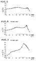
- FIGS. 6 and 7 represent the temperature characteristics of capacitances of Samples 2 and 5, respectively.
- FIG. 5 which shows the similar characteristic of Sample 1
- the characteristics of Samples 2 and 5 are far less uneven. Particularly objectionable are the peaks at high temperatures.
- the firing temperature need not be 1200° C. as in the production of Samples 1-5 but can be anywhere from the sinterable temperature of the particular ceramic material in use to less than a temperature at which Mg diffusion proceeds too fast to permit creation of the desired core-shell configuration.
- ceramic compositions composed primarily of BaTi0 3 such as the one used for Sample 1, are generally not sinterable at 1150° C., and at 1400° C. Mg diffusion is too fast to form the core-shell configuration, so that the firing temperature should be chosen from between these limits.
- the firing time is subject to change depending upon the firing temperature. Ceramics similar to those of Sample 5, not meeting the criteria of this invention, will be obtained if the firing time is as long as five hours when the firing temperature is 1250° C. The firing time at that firing temperature should therefore be up to four hours or so.
- the relative depths of the paraelectric shells depend not only on the firing temperature and firing time but also on the relative proportions of Ba and Ti in the major component, the proportion of Mg, the proportions of any other additives, the conditions of pretreatment, the firing temperature, and the profile of firing temperatures.
- the present invention specifies, therefore, that the percentage of the shell depth to the average grain size be from about five to about 30 percent,
Landscapes
- Engineering & Computer Science (AREA)
- Power Engineering (AREA)
- Manufacturing & Machinery (AREA)
- Microelectronics & Electronic Packaging (AREA)
- Compositions Of Oxide Ceramics (AREA)
- Ceramic Capacitors (AREA)
- Inorganic Insulating Materials (AREA)
Applications Claiming Priority (3)
| Application Number | Priority Date | Filing Date | Title |
|---|---|---|---|
| JP132851/97 | 1997-05-06 | ||
| JP13285197A JP3487539B2 (ja) | 1997-05-06 | 1997-05-06 | 誘電体磁器 |
| JP13285197 | 1997-05-06 |
Publications (3)
| Publication Number | Publication Date |
|---|---|
| EP0877399A2 true EP0877399A2 (de) | 1998-11-11 |
| EP0877399A3 EP0877399A3 (de) | 2000-01-05 |
| EP0877399B1 EP0877399B1 (de) | 2004-08-18 |
Family
ID=15091013
Family Applications (1)
| Application Number | Title | Priority Date | Filing Date |
|---|---|---|---|
| EP98107958A Expired - Lifetime EP0877399B1 (de) | 1997-05-06 | 1998-04-30 | Bariumtitanat-Magnesium Keramik zur Verwendung, u.a., in Kondensatoren |
Country Status (7)
| Country | Link |
|---|---|
| US (2) | US5977006A (de) |
| EP (1) | EP0877399B1 (de) |
| JP (1) | JP3487539B2 (de) |
| KR (1) | KR100279015B1 (de) |
| CN (1) | CN1100331C (de) |
| DE (1) | DE69825664T2 (de) |
| MY (1) | MY114946A (de) |
Cited By (8)
| Publication number | Priority date | Publication date | Assignee | Title |
|---|---|---|---|---|
| EP1128404A2 (de) * | 2000-02-28 | 2001-08-29 | Taiyo Yuden Co., Ltd. | Dielektrische Keramiken, keramische Vielschicht-Elektronikbauteile und Herstellungsverfahren |
| US6656865B2 (en) * | 2000-06-30 | 2003-12-02 | Taiyo Yuden Co., Ltd. | Dielectric ceramic composition and ceramic capacitor |
| EP1607989A2 (de) * | 2004-06-18 | 2005-12-21 | TDK Corporation | Keramisches Elektronikbauteil und dessen Herstellungsverfahren |
| EP1612816A1 (de) * | 2004-06-28 | 2006-01-04 | TDK Corporation | Dielektrische Zusammensetzung für einen keramischen Mehrschichtkondensator |
| EP1662522A1 (de) * | 2004-11-30 | 2006-05-31 | TDK Corporation | Dielektrische keramische Zusammensetzung mit Core-Shell Partikeln und elektronisches Gerät |
| EP1708211A2 (de) * | 2005-04-01 | 2006-10-04 | TDK Corporation | Keramischer Mehrschichtkondensator auf der Basis von Bariumtitanat oder Bariumcalciumtitanat |
| US7297403B2 (en) * | 2004-10-12 | 2007-11-20 | Tdk Corporation | Dielectric ceramic composition and electronic device |
| EP1972605A1 (de) * | 2007-03-14 | 2008-09-24 | TDK Corporation | Dielektrische keramische Zusammensetzung und elektronische Vorrichtung |
Families Citing this family (40)
| Publication number | Priority date | Publication date | Assignee | Title |
|---|---|---|---|---|
| JP2000072540A (ja) * | 1998-08-31 | 2000-03-07 | Ngk Spark Plug Co Ltd | 誘電体材料 |
| US6074971A (en) * | 1998-11-13 | 2000-06-13 | The United States Of America As Represented By The Secretary Of The Army | Ceramic ferroelectric composite materials with enhanced electronic properties BSTO-Mg based compound-rare earth oxide |
| JP3376963B2 (ja) * | 1999-06-30 | 2003-02-17 | 株式会社村田製作所 | 積層セラミックコンデンサ及びその製造方法 |
| JP3908458B2 (ja) * | 1999-12-28 | 2007-04-25 | Tdk株式会社 | 誘電体磁器組成物の製造方法 |
| KR100738760B1 (ko) * | 2000-02-16 | 2007-07-12 | 다이요 유덴 가부시키가이샤 | 적층 세라믹 콘덴서와 그 제조 방법 |
| US6785121B2 (en) * | 2000-05-30 | 2004-08-31 | Tdk Corporation | Multilayer ceramic capacitor and production method thereof |
| US6514895B1 (en) * | 2000-06-15 | 2003-02-04 | Paratek Microwave, Inc. | Electronically tunable ceramic materials including tunable dielectric and metal silicate phases |
| JP5046432B2 (ja) * | 2000-06-29 | 2012-10-10 | 京セラ株式会社 | 誘電体磁器および積層型電子部品 |
| US6673274B2 (en) | 2001-04-11 | 2004-01-06 | Cabot Corporation | Dielectric compositions and methods to form the same |
| US20030059366A1 (en) * | 2001-09-21 | 2003-03-27 | Cabot Corporation | Dispersible barium titanate-based particles and methods of forming the same |
| JP4446324B2 (ja) * | 2001-09-27 | 2010-04-07 | 株式会社村田製作所 | 誘電体磁器組成物及びそれを用いたコンデンサ |
| DE60335427D1 (de) | 2002-01-15 | 2011-02-03 | Tdk Corp | Dielektrische keramische Zusammensetzung und elektronische Vorrichtung |
| US20030215606A1 (en) * | 2002-05-17 | 2003-11-20 | Clancy Donald J. | Dispersible dielectric particles and methods of forming the same |
| KR100466072B1 (ko) * | 2002-05-24 | 2005-01-13 | 삼성전기주식회사 | 적층 세라믹 콘덴서용 유전체 조성물 및 이를 이용한 적층세라믹 콘덴서 |
| KR100479415B1 (ko) * | 2002-06-08 | 2005-03-30 | 학교법인 한양학원 | 표면개질된 티탄산바륨의 제조방법 및 적층 세라믹 콘덴서 제조용 슬러리의 제조방법 |
| US20040014588A1 (en) * | 2002-07-19 | 2004-01-22 | Van Iersel Godefridus J.F.A. | Npo dielectric compositions |
| US20040052721A1 (en) * | 2002-09-13 | 2004-03-18 | Kerchner Jeffrey A. | Dielectric particles having passivated surfaces and methods of forming same |
| US20040121153A1 (en) * | 2002-12-20 | 2004-06-24 | Sridhar Venigalla | High tetragonality barium titanate-based compositions and methods of forming the same |
| FR2861088B1 (fr) * | 2003-10-13 | 2006-01-20 | Centre Nat Rech Scient | Procede d'obtention d'un materiau composite ferroelectrique |
| JP4661203B2 (ja) * | 2004-12-15 | 2011-03-30 | Tdk株式会社 | セラミック電子部品およびその製造方法 |
| JP4483597B2 (ja) * | 2005-01-20 | 2010-06-16 | Tdk株式会社 | 電子部品、誘電体磁器組成物およびその製造方法 |
| JP4937522B2 (ja) * | 2005-04-04 | 2012-05-23 | Tdk株式会社 | 電子部品、誘電体磁器組成物およびその製造方法 |
| JP4936850B2 (ja) | 2006-09-15 | 2012-05-23 | 太陽誘電株式会社 | 積層セラミックコンデンサ |
| JP5078307B2 (ja) * | 2006-09-27 | 2012-11-21 | 京セラ株式会社 | 誘電体磁器およびその製法、ならびにコンデンサ |
| WO2008105240A1 (ja) * | 2007-02-26 | 2008-09-04 | Murata Manufacturing Co., Ltd. | 誘電体セラミック、及び積層セラミックコンデンサ |
| JP4858248B2 (ja) * | 2007-03-14 | 2012-01-18 | Tdk株式会社 | 誘電体磁器組成物および電子部品 |
| JP5023748B2 (ja) * | 2007-03-14 | 2012-09-12 | Tdk株式会社 | 誘電体磁器組成物および電子部品 |
| JP5132972B2 (ja) * | 2007-04-09 | 2013-01-30 | 太陽誘電株式会社 | 誘電体セラミックス及びその製造方法並びに積層セラミックコンデンサ |
| JP5109872B2 (ja) | 2008-08-27 | 2012-12-26 | 株式会社村田製作所 | 積層セラミックコンデンサおよびその製造方法 |
| WO2010140868A2 (ko) * | 2009-06-05 | 2010-12-09 | 씨큐브 주식회사 | 산화물층이 코팅된 티탄산바륨 분말 및 그의 제조 방법 |
| CN102459083A (zh) * | 2009-06-05 | 2012-05-16 | Cqv株式会社 | 涂敷有氧化物层的钛酸钡粉末及其制备方法 |
| JP5018839B2 (ja) * | 2009-07-22 | 2012-09-05 | 株式会社村田製作所 | 誘電体セラミックおよび積層セラミックコンデンサ |
| JP5548924B2 (ja) * | 2009-11-06 | 2014-07-16 | Tdk株式会社 | 誘電体磁器組成物および電子部品 |
| CN102153351B (zh) * | 2010-12-03 | 2013-03-13 | 中国兵器工业第五二研究所 | 一种添加B2O3-Li2CO3助烧剂低温烧结制备钛酸锶钡钙复相陶瓷的方法 |
| JP5372034B2 (ja) * | 2011-01-24 | 2013-12-18 | 京セラ株式会社 | 誘電体磁器および積層型電子部品 |
| CN105453201B (zh) * | 2013-07-30 | 2018-10-02 | 京瓷株式会社 | 电介质膜、膜电容器以及电子设备 |
| JP6502092B2 (ja) * | 2014-12-26 | 2019-04-17 | 太陽誘電株式会社 | 積層セラミックコンデンサ |
| JP6711840B2 (ja) * | 2015-10-28 | 2020-06-17 | 京セラ株式会社 | コンデンサ |
| KR102483896B1 (ko) * | 2017-12-19 | 2022-12-30 | 삼성전자주식회사 | 세라믹 유전체 및 그 제조 방법, 세라믹 전자 부품 및 전자장치 |
| JP2022098294A (ja) * | 2020-12-21 | 2022-07-01 | Tdk株式会社 | 誘電体磁器組成物および電子部品 |
Citations (1)
| Publication number | Priority date | Publication date | Assignee | Title |
|---|---|---|---|---|
| EP0504756A1 (de) * | 1991-03-16 | 1992-09-23 | Taiyo Yuden Co., Ltd. | Keramischer Kondensator und seine Herstellungsmethode |
Family Cites Families (5)
| Publication number | Priority date | Publication date | Assignee | Title |
|---|---|---|---|---|
| US5312790A (en) * | 1993-06-09 | 1994-05-17 | The United States Of America As Represented By The Secretary Of The Army | Ceramic ferroelectric material |
| GB9504443D0 (en) * | 1995-03-06 | 1995-04-26 | Cookson Group Plc | Temperature stable dielectric |
| US5646080A (en) * | 1995-11-20 | 1997-07-08 | Tam Ceramics, Inc. | Dielectric stable at high temperature |
| US5801112A (en) * | 1996-06-14 | 1998-09-01 | Kyocera Corporation | Dielectric ceramic composition |
| JP3282520B2 (ja) * | 1996-07-05 | 2002-05-13 | 株式会社村田製作所 | 積層セラミックコンデンサ |
-
1997
- 1997-05-06 JP JP13285197A patent/JP3487539B2/ja not_active Expired - Lifetime
-
1998
- 1998-04-30 EP EP98107958A patent/EP0877399B1/de not_active Expired - Lifetime
- 1998-04-30 DE DE69825664T patent/DE69825664T2/de not_active Expired - Lifetime
- 1998-05-04 KR KR1019980015903A patent/KR100279015B1/ko not_active IP Right Cessation
- 1998-05-05 MY MYPI98001998A patent/MY114946A/en unknown
- 1998-05-06 CN CN98114815A patent/CN1100331C/zh not_active Expired - Lifetime
- 1998-05-06 US US09/072,789 patent/US5977006A/en not_active Expired - Lifetime
-
1999
- 1999-09-13 US US09/394,729 patent/US6087287A/en not_active Expired - Lifetime
Patent Citations (1)
| Publication number | Priority date | Publication date | Assignee | Title |
|---|---|---|---|---|
| EP0504756A1 (de) * | 1991-03-16 | 1992-09-23 | Taiyo Yuden Co., Ltd. | Keramischer Kondensator und seine Herstellungsmethode |
Cited By (17)
| Publication number | Priority date | Publication date | Assignee | Title |
|---|---|---|---|---|
| EP1128404A2 (de) * | 2000-02-28 | 2001-08-29 | Taiyo Yuden Co., Ltd. | Dielektrische Keramiken, keramische Vielschicht-Elektronikbauteile und Herstellungsverfahren |
| EP1128404A3 (de) * | 2000-02-28 | 2003-08-06 | Taiyo Yuden Co., Ltd. | Dielektrische Keramiken, keramische Vielschicht-Elektronikbauteile und Herstellungsverfahren |
| US6656865B2 (en) * | 2000-06-30 | 2003-12-02 | Taiyo Yuden Co., Ltd. | Dielectric ceramic composition and ceramic capacitor |
| EP1607989A2 (de) * | 2004-06-18 | 2005-12-21 | TDK Corporation | Keramisches Elektronikbauteil und dessen Herstellungsverfahren |
| US7538057B2 (en) | 2004-06-18 | 2009-05-26 | Tdk Corporation | Ceramic electronic device and the production method |
| EP1607989A3 (de) * | 2004-06-18 | 2008-06-04 | TDK Corporation | Keramisches Elektronikbauteil und dessen Herstellungsverfahren |
| EP1612816A1 (de) * | 2004-06-28 | 2006-01-04 | TDK Corporation | Dielektrische Zusammensetzung für einen keramischen Mehrschichtkondensator |
| US7061748B2 (en) | 2004-06-28 | 2006-06-13 | Tdk Corporation | Multilayer ceramic capacitor |
| US7297403B2 (en) * | 2004-10-12 | 2007-11-20 | Tdk Corporation | Dielectric ceramic composition and electronic device |
| US7381464B2 (en) | 2004-11-30 | 2008-06-03 | Tdk Corporation | Dielectric ceramic composition and electronic device |
| EP2003665A1 (de) * | 2004-11-30 | 2008-12-17 | TDK Corporation | Dielektrische keramische Zusammensetzung und elektronische Vorrichtung |
| EP1662522A1 (de) * | 2004-11-30 | 2006-05-31 | TDK Corporation | Dielektrische keramische Zusammensetzung mit Core-Shell Partikeln und elektronisches Gerät |
| EP1708211A2 (de) * | 2005-04-01 | 2006-10-04 | TDK Corporation | Keramischer Mehrschichtkondensator auf der Basis von Bariumtitanat oder Bariumcalciumtitanat |
| EP1708211A3 (de) * | 2005-04-01 | 2008-06-11 | TDK Corporation | Keramischer Mehrschichtkondensator auf der Basis von Bariumtitanat oder Bariumcalciumtitanat |
| US7528088B2 (en) | 2005-04-01 | 2009-05-05 | Tdk Corporation | Electronic device |
| EP1972605A1 (de) * | 2007-03-14 | 2008-09-24 | TDK Corporation | Dielektrische keramische Zusammensetzung und elektronische Vorrichtung |
| US8192851B2 (en) | 2007-03-14 | 2012-06-05 | Tdk Corporation | Dielectric ceramic composition and electronic device |
Also Published As
| Publication number | Publication date |
|---|---|
| JPH10308321A (ja) | 1998-11-17 |
| MY114946A (en) | 2003-02-28 |
| KR100279015B1 (ko) | 2001-01-15 |
| US6087287A (en) | 2000-07-11 |
| DE69825664D1 (de) | 2004-09-23 |
| EP0877399A3 (de) | 2000-01-05 |
| CN1204846A (zh) | 1999-01-13 |
| CN1100331C (zh) | 2003-01-29 |
| US5977006A (en) | 1999-11-02 |
| JP3487539B2 (ja) | 2004-01-19 |
| EP0877399B1 (de) | 2004-08-18 |
| KR19980086731A (ko) | 1998-12-05 |
| DE69825664T2 (de) | 2005-08-25 |
Similar Documents
| Publication | Publication Date | Title |
|---|---|---|
| EP0877399B1 (de) | Bariumtitanat-Magnesium Keramik zur Verwendung, u.a., in Kondensatoren | |
| US8154851B2 (en) | Dielectric ceramic, manufacturing method thereof, and multilayer ceramic capacitor | |
| US7365958B2 (en) | Dielectric ceramics, multilayer ceramic capacitor and method for manufacturing the same | |
| EP1792880B1 (de) | Dielektrische keramische Zusammensetzung, elektronische Vorrichtung und keramischer Vielschichtkondensator | |
| EP1648004B1 (de) | Dielektrische keramische Zusammensetzung mit dielektrischen Kern-Hülle Partikeln und elektronisches Gerät | |
| EP1786005B1 (de) | Dielektrische Keramikzusammensetzung, Elektronikbauteil und keramischer Mehrschichtkondensator | |
| KR100414331B1 (ko) | 비환원성 유전체 세라믹 및 이것을 사용한 모놀리식 세라믹 커패시터 | |
| EP0534378B1 (de) | Nichtreduzierbare dielektrische keramische Zusammensetzung | |
| JPH05152158A (ja) | セラミツクコンデンサ | |
| US5130281A (en) | Dielectric ceramic compositions and manufacturing method of dielectric ceramics | |
| JP2003040671A (ja) | 誘電体磁器及び積層型電子部品並びに積層型電子部品の製法 | |
| US5672378A (en) | Method for making a BaTiO3 powder mixture the powder mixture and method for making a Y5V ceramic body therefrom | |
| US6423243B2 (en) | Manganese-zinc base ferrite | |
| KR100673878B1 (ko) | 유전체 자기 조성물, 전자 부품 및 이들의 제조 방법 | |
| US5361187A (en) | Ceramic dielectric compositions and capacitors produced therefrom | |
| EP0121161B1 (de) | Keramische Zusammensetzung mit hoher Dielektrizitätskonstante | |
| US4723193A (en) | Low temperature sintered ceramic capacitor with a temperature compensating capability, and method of manufacture | |
| KR20140118557A (ko) | 유전체 자기 조성물 및 이를 포함하는 적층 세라믹 캐패시터 | |
| US5103369A (en) | Solid dielectric capacitor | |
| JP2006156450A (ja) | 積層セラミックコンデンサおよびその製法 | |
| JP4508858B2 (ja) | 積層セラミックコンデンサおよびその製法 | |
| JP2002284571A (ja) | 温度特性及びdcバイアス特性に優れた誘電体磁器 | |
| KR20060135304A (ko) | 저온 소성용 유전체 분말의 제조 방법과 이를 이용한 적층세라믹 콘덴서의 제조 방법 | |
| US4700267A (en) | Low temperature sintered ceramic capacitor with a temperature compensating capability, and method of manufacture | |
| JP2006179675A (ja) | 積層セラミックコンデンサおよびその製法 |
Legal Events
| Date | Code | Title | Description |
|---|---|---|---|
| PUAI | Public reference made under article 153(3) epc to a published international application that has entered the european phase |
Free format text: ORIGINAL CODE: 0009012 |
|
| AK | Designated contracting states |
Kind code of ref document: A2 Designated state(s): DE GB NL |
|
| AX | Request for extension of the european patent |
Free format text: AL;LT;LV;MK;RO;SI |
|
| PUAL | Search report despatched |
Free format text: ORIGINAL CODE: 0009013 |
|
| AK | Designated contracting states |
Kind code of ref document: A3 Designated state(s): AT BE CH CY DE DK ES FI FR GB GR IE IT LI LU MC NL PT SE |
|
| AX | Request for extension of the european patent |
Free format text: AL;LT;LV;MK;RO;SI |
|
| 17P | Request for examination filed |
Effective date: 20000406 |
|
| AKX | Designation fees paid |
Free format text: DE GB NL |
|
| GRAP | Despatch of communication of intention to grant a patent |
Free format text: ORIGINAL CODE: EPIDOSNIGR1 |
|
| GRAS | Grant fee paid |
Free format text: ORIGINAL CODE: EPIDOSNIGR3 |
|
| GRAA | (expected) grant |
Free format text: ORIGINAL CODE: 0009210 |
|
| AK | Designated contracting states |
Kind code of ref document: B1 Designated state(s): DE GB NL |
|
| REG | Reference to a national code |
Ref country code: GB Ref legal event code: FG4D |
|
| REF | Corresponds to: |
Ref document number: 69825664 Country of ref document: DE Date of ref document: 20040923 Kind code of ref document: P |
|
| PLBE | No opposition filed within time limit |
Free format text: ORIGINAL CODE: 0009261 |
|
| STAA | Information on the status of an ep patent application or granted ep patent |
Free format text: STATUS: NO OPPOSITION FILED WITHIN TIME LIMIT |
|
| 26N | No opposition filed |
Effective date: 20050519 |
|
| PGFP | Annual fee paid to national office [announced via postgrant information from national office to epo] |
Ref country code: NL Payment date: 20120425 Year of fee payment: 15 |
|
| PGFP | Annual fee paid to national office [announced via postgrant information from national office to epo] |
Ref country code: GB Payment date: 20120419 Year of fee payment: 15 |
|
| REG | Reference to a national code |
Ref country code: NL Ref legal event code: V1 Effective date: 20131101 |
|
| GBPC | Gb: european patent ceased through non-payment of renewal fee |
Effective date: 20130430 |
|
| PG25 | Lapsed in a contracting state [announced via postgrant information from national office to epo] |
Ref country code: GB Free format text: LAPSE BECAUSE OF NON-PAYMENT OF DUE FEES Effective date: 20130430 |
|
| PG25 | Lapsed in a contracting state [announced via postgrant information from national office to epo] |
Ref country code: NL Free format text: LAPSE BECAUSE OF NON-PAYMENT OF DUE FEES Effective date: 20131101 |
|
| REG | Reference to a national code |
Ref country code: DE Ref legal event code: R082 Ref document number: 69825664 Country of ref document: DE Representative=s name: WEICKMANN & WEICKMANN PATENT- UND RECHTSANWAEL, DE Ref country code: DE Ref legal event code: R082 Ref document number: 69825664 Country of ref document: DE Representative=s name: WEICKMANN & WEICKMANN PATENTANWAELTE - RECHTSA, DE Ref country code: DE Ref legal event code: R082 Ref document number: 69825664 Country of ref document: DE Representative=s name: PATENTANWAELTE WEICKMANN & WEICKMANN, DE |
|
| PGFP | Annual fee paid to national office [announced via postgrant information from national office to epo] |
Ref country code: DE Payment date: 20170426 Year of fee payment: 20 |
|
| REG | Reference to a national code |
Ref country code: DE Ref legal event code: R071 Ref document number: 69825664 Country of ref document: DE |