EP0862829B1 - Bildsensor mit linearem ausgang mit grossem dynamikbereich - Google Patents
Bildsensor mit linearem ausgang mit grossem dynamikbereich Download PDFInfo
- Publication number
- EP0862829B1 EP0862829B1 EP96942754A EP96942754A EP0862829B1 EP 0862829 B1 EP0862829 B1 EP 0862829B1 EP 96942754 A EP96942754 A EP 96942754A EP 96942754 A EP96942754 A EP 96942754A EP 0862829 B1 EP0862829 B1 EP 0862829B1
- Authority
- EP
- European Patent Office
- Prior art keywords
- pixel
- integration
- buffer
- signals
- readout
- Prior art date
- Legal status (The legal status is an assumption and is not a legal conclusion. Google has not performed a legal analysis and makes no representation as to the accuracy of the status listed.)
- Expired - Lifetime
Links
Images


Classifications
-
- H—ELECTRICITY
- H04—ELECTRIC COMMUNICATION TECHNIQUE
- H04N—PICTORIAL COMMUNICATION, e.g. TELEVISION
- H04N23/00—Cameras or camera modules comprising electronic image sensors; Control thereof
- H04N23/70—Circuitry for compensating brightness variation in the scene
-
- H—ELECTRICITY
- H04—ELECTRIC COMMUNICATION TECHNIQUE
- H04N—PICTORIAL COMMUNICATION, e.g. TELEVISION
- H04N25/00—Circuitry of solid-state image sensors [SSIS]; Control thereof
- H04N25/50—Control of the SSIS exposure
- H04N25/53—Control of the integration time
- H04N25/533—Control of the integration time by using differing integration times for different sensor regions
-
- H—ELECTRICITY
- H04—ELECTRIC COMMUNICATION TECHNIQUE
- H04N—PICTORIAL COMMUNICATION, e.g. TELEVISION
- H04N25/00—Circuitry of solid-state image sensors [SSIS]; Control thereof
- H04N25/50—Control of the SSIS exposure
- H04N25/57—Control of the dynamic range
- H04N25/58—Control of the dynamic range involving two or more exposures
- H04N25/587—Control of the dynamic range involving two or more exposures acquired sequentially, e.g. using the combination of odd and even image fields
-
- H—ELECTRICITY
- H04—ELECTRIC COMMUNICATION TECHNIQUE
- H04N—PICTORIAL COMMUNICATION, e.g. TELEVISION
- H04N25/00—Circuitry of solid-state image sensors [SSIS]; Control thereof
- H04N25/70—SSIS architectures; Circuits associated therewith
- H04N25/71—Charge-coupled device [CCD] sensors; Charge-transfer registers specially adapted for CCD sensors
- H04N25/75—Circuitry for providing, modifying or processing image signals from the pixel array
-
- H—ELECTRICITY
- H04—ELECTRIC COMMUNICATION TECHNIQUE
- H04N—PICTORIAL COMMUNICATION, e.g. TELEVISION
- H04N25/00—Circuitry of solid-state image sensors [SSIS]; Control thereof
- H04N25/70—SSIS architectures; Circuits associated therewith
- H04N25/76—Addressed sensors, e.g. MOS or CMOS sensors
- H04N25/767—Horizontal readout lines, multiplexers or registers
-
- H—ELECTRICITY
- H04—ELECTRIC COMMUNICATION TECHNIQUE
- H04N—PICTORIAL COMMUNICATION, e.g. TELEVISION
- H04N25/00—Circuitry of solid-state image sensors [SSIS]; Control thereof
- H04N25/70—SSIS architectures; Circuits associated therewith
- H04N25/76—Addressed sensors, e.g. MOS or CMOS sensors
- H04N25/77—Pixel circuitry, e.g. memories, A/D converters, pixel amplifiers, shared circuits or shared components
Definitions
- the present invention relates to semiconductor image sensors, and more specifically, to a system and method of extending dynamic range in CMOS active pixel sensor circuits.
- EP 0599570 describes an imaging device comprising an array of sensing elements in which a timing difference between two field shift pulses in the same vertical blanking period is used to control each of two different charge accumulation periods for each sensing element to provide for expanded dynamic range.
- US 5264944 describes a CCD camera system in which an electronic iris control circuit controls an opening time of an iris in front of a sensor array to block the array to achieve different integration times in different frames.
- US 4819070 describes a CCD image sensor array that can sequentially select two separate rows of pixels within the same horizontal blanking period to produce a desired integration time.
- US 5274459 describes a CCD solid state image sensing device having a plurality of photo-sensing sections arranged in a two dimensional array.
- An active pixel sensor is a special kind of light sensing device. Each active pixel includes a light sensing element and one or more active transistors within the pixel itself. The active transistors amplify and buffer the signals generated by the light sensing elements in the pixels.
- One type of such APS device is disclosed in US Patent No. 5,471,515 by Fossum et al.
- APS devices represent an emerging technology in a wide range of imaging applications. APS devices have a number of significant advantages in comparison with the well-developed and widely used charge coupled devices (CCDs). Because of the number of stages in a CCD, a nearly perfect charge transfer efficiency must be maintained in a CCD in order to maintain good signal fidelity. This usually makes CCDs susceptible to damage from both ionizing and displacement damage. In particular, the displacement damage caused by high-energy particles and photons may prove to be deadly to CCDs.
- CCDs charge coupled devices
- CCD arrays present engineering difficulties in manufacturing. Device miniaturization is difficult with CCD devices since the extreme requirements of CCDs necessitate a special formation process. This formation process prevents CCDs from being easily integrated with on-chip integrated circuits such as complementary-metal-oxide-semiconductor (CMOS) integrated circuits. CCDs also suffer limited spectral responsivity range and readout rates. Furthermore, the readout of CCDs is destructive, i.e., their stored value is destroyed upon reading out. Implementation of the nondestructive readout in a CCD device is difficult.
- CMOS complementary-metal-oxide-semiconductor
- an APS device receives and processes input signals with the active pixel itself, thus eliminating the charge transfer over distances that are inherent in CCDs. Consequently, many drawbacks associated with CCDs are avoided in APS devices. For example, the performance of APS devices can be maintained as the array size increases. The APS readout rate is usually higher than that of CCDs. Since CMOS circuitry is often associated with the image sensor, the power consumption can be significantly reduced. APS devices are inherently compatible with CMOS processes, allowing reduced cost of manufacturing. Many on-chip operations and controls can be relatively easily implemented including timing and analog-to-digital conversion. APS devices are also less vulnerable to radiation damage and can be designed for non-destructive readout. Moreover, the active pixels of APS devices allow random access and on-chip signal processing.
- SNR signal-to-noise ratio
- a large dynamic range is desirable in applications for sensing low light signals and capturing images with large variations in brightness.
- CMOS-based APS circuits The dynamic range of previously-reported CMOS-based APS circuits has been limited by both the saturation level of the signal chain circuit, which is typically about 1.2 volts for a 5-volt power supply, and the noise floor of the sensor, which is typically about 150 ⁇ V. This results in a dynamic range of approximately 78dB (13 bits), which is comparable to the dynamic range of the state-of-art CCD devices.
- the output voltage signal of an imaging device is dependent on the input light level, the efficiency of the optical coupling device and the detector characteristics including the quantum efficiency, the effective active sensing area, the integration time, and the electrical conversion gain of volts/electron.
- the output signal can be approximately expressed as the following: V out ⁇ ⁇ 4 f 2 ⁇ optics A det T int ⁇ G , where ⁇ is the incident photon flux, f is the f-stop of the coupling optical system, ⁇ optics is the transmission of the optical system, A det is the pixel size, T int is the integration time, ⁇ is the pixel quantum efficiency, and G is the conversion gain in volts/electron.
- the typical values for a APS device are f/8, 80% for ⁇ optics , 20 ⁇ m for A det , 33ms for T int , 25% in ⁇ , and G ⁇ 10 ⁇ V/e, respectively.
- the exposure of an imaging device for a given hardware configuration is usually controlled by changing either the aperture (i.e., f-stop) or the integration time. If the input light level is low, the integration time is increased to improve the signal-to-noise ratio. If the input light is bright, the integration time is reduced to avoid saturation of the detector while maintaining a high SNR. The lower limit of the integration time is set by the readout time.
- the integration time of a CMOS APS device with N rows of pixels can be controlled by resetting a row of pixels in advance of readout. If the readout time for one row of pixels is T row , the total frame readout time is NT row . Since the pixels of a row are reset for a new integration upon readout, the integration time is simply the frame time NT row .
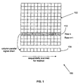
- FIG. 1 illustrates an exemplary APS.
- a pixel array 102 has N rows of pixels with each row having M columns.
- a column-parallel signal chain 104 such as a sampling capacitor bank with M storage cells is used for readout.
- a particular row is selected for readout at one time.
- the sensor data from the M pixels in the selected row is copied onto the capacitor bank 104.
- the copy process also resets the pixels in the selected row and begins a new integration.
- the M storage cells in the capacitor bank 104 are then scanned sequentially for readout.
- the above readout process is then repeated for the next row. Therefore, the integration time for each pixel is identical and is equal to the readout time of a frame, i.e., NT row .
- the inventors of the present invention recognized a limitation of the above two methods in that the exposure remains the same for the entire image. This can result in distortion of the detected images in some circumstances. For example, an outdoor scene might be optimally exposed for the sunlit areas but overexposed in the shadowed areas. This can result in loss of detail in shadowed areas.
- a nonlinear output sensor is designed to have a high differential gain for light levels, and low differential gain for high light levels. It is desirable that the nonlinear gain be achieved within each pixel. As a result, pixel to pixel variations in the transfer function can lead to unacceptable values of fixed pattern noise.
- Another approach is to implement multiple storage sites in each pixel in CCD devices to record different integration signals from the same pixel.
- one storage site corresponds to a short integration period and the second to a long integration period, thus increasing the dynamic range.
- the readout data can be transformed to a lower bit count encoding using nonlinear techniques for display, storage, and transmission.
- One limitation of this technique is a decreased readout rate since the readout time may be doubled since twice as much of the amount of data may need to be read.
- Another limitation is the reduced fill factor since two storage sites occupy considerable pixel area.
- the present invention describes a new technique in APS sensors and operation methods thereof to increase their dynamic ranges.
- at least two different integration times are obtained for each active pixel.
- One or more column-parallel signal chains are used to implement the multiple integration times for each active pixel.
- each pixel is sampled multiple times during a single frame readout, thus resulting in multiple integration times.
- Another aspect of the present invention increases the frame rate by using more than one column-parallel signal chain to achieve multiple data points of different integration times for each pixel.
- a maximal frame rate is achieved for a given APS device by having the number of column-parallel signal chains match the number of different integration times.
- a preferred operation mode of such system in accordance with the present invention includes simultaneously copying multiple columns into the column-parallel signal chains and subsequently reading out all the column-parallel signal chains simultaneously with each being scanned in a sequential manner.
- the frame rate is increased by a factor equal to the number of the column-parallel signal chains as compared with achieving the same number of integration times with a single column-parallel signal chain for readout.
- the dynamic range of the APS device is thus extended by a factor given by the ratio of the longest integration time versus the shortest integration time.
- a new readout method is also described. This method can be used to improve the dynamic range of a conventional APS device having a single column-parallel signal chain by achieving multiple integration times for each active pixel. Special advantages are obtained when used with non-destructive readout of an APS device in achieving multiple integration times of each pixel.
- Another aspect incorporates digital processors including analog-to-digital converters in the column-parallel signal chains.
- On-chip buffer memory units and/or multiple source followers may be used for each pixel to further enhance the flexibility and performance of the systems in accordance with the present invention.
- CMOS APS devices as an example for implementation. However, it should be understood that the method and design can also be implemented in other active pixel sensors, and may be usable in other image acquiring systems.
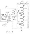
- FIG. 2 illustrates the first preferred embodiment 200 of the present invention.
- An active pixel array 202 has N rows and M columns, hence with a total of NxM pixels.
- Each pixel comprises a light sensing element and one or more active transistors.
- the active transistors amplify and buffer the signals generated by the light sensing element in the pixel.
- Each active pixel has one output source follower that is connected to the corresponding column bus.
- Each of the signal chains, 204 and 206 has M storage cells for temporarily storing the electrical signals from the pixels being read.
- the column-parallel signal chains 204 and 206 can be implemented with capacitor banks for analog processing and analog-to-digital converters (ADCs) for digital processing or any other device that is capable of storing image information.
- ADCs analog-to-digital converters
- the device 200 also includes an control circuit (not shown) having row and column decoders for addressing the proper row/column of pixels, clock generator circuits for synchronization, and readout circuits.
- the control circuit is operable to control the readout of the pixels and the operation of the column-parallel signal chain(s) in a desired sequence with desired integration time(s).
- FIG. 3 shows the active pixel 302 including a photogate 310, a DC biased transfer gate 311, an output floating diffusion 314, a reset transistor 315, a drain diffusion 316, a gate source follower 317, and a row selection transistor 318.
- the circuit 304 represents a storage cell shared by a column of active pixels.
- the storage cell 304 includes a load transistor 320, a first output circuit 321 for buffering and exporting the reset level, and a second output circuit 322 for buffering and exporting the signal level.
- each active pixel of a column is connected to two such storage cells substantially similar to 304. It should be understood that other designs of the active pixel and column storage cell can also be used in accordance with the present invention.
- a row of pixels in the active pixel array 202 e.g., the row n 210
- the signals representing the M pixels of the row n 210 are copied simultaneously to the corresponding M storage cells in the first column-parallel signal chain 204.
- the time duration of the copying process is T copy , typically about 1-10 ⁇ s for an APS device.
- the copying process also resets the pixels in the row n 210 and a new integration in the row n 210 is started.
- the signals of M pixels in another row 220 that is shifted by ⁇ rows relative to row 210 are simultaneously copied to the corresponding M storage cells in the second column-parallel signal chain 206 during time T copy and the pixels in the row (n- ⁇ ) 220 are subsequently reset for another integration.
- the M storage cells in each of the first column-parallel signal chain 204 and the second column-parallel signal chain 206 are simultaneously and respectively scanned for readout.
- the M storage cells in each column-parallel signal chain are sequentially scanned and the signals therein are read out. This completes the readout of the row n 210 and row (n- ⁇ ) 220.
- the time for scanning and reading one pixel is T scan , which is typically between 100ns-10 ⁇ s. Then, the next two rows are selected for readout in the same fashion. Therefore, a single row readout process reads two separated rows of pixels.
- the above readout process repeats until every row in the active pixel array 202 is read to complete a frame. This results in two sets of data from every active pixel in the array 202, one from the first column-parallel signal chain 204 and another one from the second column-parallel signal chain 206, respectively.
- the two sets of data have different integration times and the two data points for the same pixel are read out at different times by a time lag of the time for a row readout process multiplied by ⁇ .
- T row 2 T copy +MT scan , comparing to ( T copy +MT scan ) in a row readout in the prior-art system as in FIG. 1.
- T frame NT row .
- the integration time for each pixel is the same and is the readout time for a frame.
- the two sets of readout from the two column-parallel signal chains 204 and 206 in the system of FIG. 2 have different integration times.
- the dynamic range D 2 of the active pixel sensor 200 is improved over the dynamic range D 1 of the system 100 by a factor of T 1int /T 2int :
- D 2 ( dB ) log( T 1int T 2in t ) +D 1 ( dB );
- D 2 ( bits ) log 2 ( T 1int T 2int ) +D 1 ( bits ).
- the detected image is reconstructed by reading out the bright portions of the image with the data of short integration time T 2int from the second column-parallel signal chain 206. Conversely, darker portions of the image are read out using the data of long integration time T 1int from the first column-parallel signal chain 204. Therefore, portions of a scene which appear saturated by the long integration time T 1int can be managed by using the short integration time T 2int .
- the second embodiment of the present invention uses the readout technique for the system 200 of FIG. 2 in the system 100 of FIG. 1 to extend the dynamic range.
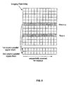
- the readout sequence is illustrated in FIG. 4.
- the row n of pixels 110 in the active pixel array 102 is first selected for readout.
- the signals in the M pixels of the row n 110 are then copied simultaneously to the corresponding M storage cells in the column-parallel signal chain 104.
- the copying process also resets the pixels in the row n 110 and begins a new integration in the row n 110.
- the M storage cells of the column-parallel signal chain 104 is sequentially scanned and the signals therein are read out.
- the signals of M pixels of another row(n- ⁇ ) 402 are simultaneously copied to the corresponding M storage cells in the column-parallel signal chain 104.
- the row 402 is displaced from the row 110 by ⁇ number of rows.
- the pixels in the row (n- ⁇ ) 402 are subsequently reset for another integration.
- the above process then repeats for row (n+1) and row (n- ⁇ +1), etc. until all N rows of active pixels in the array 102 are processed.
- Two data points of different integration times from the same pixel are read out at two different times.
- the increase in the dynamic range is essentially the same as in the first embodiment using a sensor design 200 of two column-parallel signal chains although the integration times are different.
- the second embodiment has an additional advantage of being compatible with previously-fabricated CMOS APS sensors with single column-parallel signal chain but has a reduced frame rate for readout due to the increased readout time per frame.
- a third embodiment implements more than two integration times in an active pixel array.
- k column-parallel signal chains can be implemented and used in a similar way as in the first embodiment 200. k rows of pixels are read out simultaneously and stored in the k column-parallel signal chains, respectively. The k column-parallel signal chains are subsequently scanned and read out simultaneously. Thus, the frame time is reduced by approximately a factor of k while achieving essentially similar dynamic range increase comparing to the use of a single column-parallel signal chain for k integration times.
- an intermediate number of column-parallel signal chains between 1 and k can be used to produce a desired set of k integration times and a frame rate tailored for a specific application. At least one of the column-parallel chains is used to obtain at least two sets of data with different integration times.
- the above embodiments contemplate using a destructive readout, wherein an active pixel is reset for another integration after the signal therein is copied and read out.
- One advantage of the destructive readout is that the on-chip correlated doubling sampling can be implemented in many active pixel sensors to suppress noise such as the fixed patten noise and the kTC noise. This is disclosed by Mendis et al. in "CMOS Active Pixel Image Sensor", IEEE Transactions On Electron Devices, Vol.41(3),pp.452-453, March, 1994.
- a non-destructive readout can also be used with the above embodiments for an increased dynamic range and possibly increased speed. Each pixel continues to integrate the signal and the pixel value is copied and read out without resetting.
- ADC High Performance Analog-to-Digital Converter
- a high speed ADC with a high resolution can be made using the described techniques of the present invention.
- the multiple data points generated from each pixel can be converted from analog to digital with multiple ADCs with each data point being processed by one ADC. This can generate both a high resolution conversion by combining the bits from each data point and a fast conversion speed since the multiple ADCs operate in parallel.
- the architecture shown in FIG. 1 with a readout of four data points per pixel can be used for such a ADC.
- an ADC word length of 12 bits can be generated by patching the four outputs of the ADCs together.
- the time domain which can be accurately controlled, is used to provide the effective gain of 8x between each of the four data points. This is shown in Table 1.
- Each of the four ADCs is shown as a single slope ADC, with an increment of 0.250mV per step and a total of 8 levels.
- the time required for each conversion is 8 cycles. Since the four ADCs can be operated in parallel, the total time to achieve the 12-bit resolution could remain as 8 cycles. Typically, each cycle is of the order 1 ⁇ s so that a complete conversion can be finished in 8 ⁇ s.
- the bits from the four ADCs corresponding to four data points are reassembled externally to generate the 12-bit output.
- n-bit dynamic range is not equivalent to obtaining n-bit resolution.
- the sensor of the above-described case could be saturated for the three long integration times for a given light intensity at a pixel, thus only the data with the shortest integration time is used.
- One way to improve the number of significant digits is to use a higher resolution ADC to have some overlap in conversion range.
- the techniques of the embodiments described use readout units of rows and column-parallel readout chains.
- readout units could be other pixel blocks, such as neighboring pixel patches (e.g., 7x7 pixel areas), or any other desired shape.
- the readout chains can be changed to accommodate the choice of readout units. While the embodiments describe obtaining two integration signals for each pixel being stored, it should be understood that any number, e.g., 3 or 4, integration times could be used. Additional column-parallel signal chains may be added to maintain the frame rate while increasing the number of integration times. Alternatively, the chip design can be maintained at a price of a slower frame rate to increase the number of integration times using the readout method of the present invention.
Claims (23)
- Bildgebungsvorrichtung (200) mit:wobei die Bildgebungsvorrichtung gekennzeichnet ist durch:einem Substrat, das aus einem Halbleitermaterial gebildet ist;einem Bilddetektorarray (202) mit einer Mehrzahl von Pixelschaltungen (302), die auf dem Substrat gebildet sind, wobei jede Pixelschaltung ein Pixelsignal erzeugt, das ein Pixel eines Bildes anzeigt; undeinem ersten Signalpuffer (304,204), der auf dem Substrat gebildet und mit dem Bilddetektorarray gekoppelt ist, wobei der erste Signalpuffer Pufferzellen hat, die zum Speichern jeweiliger Pixelsignale von einer ersten Gruppe (210) der Pixelschaltungen verbindbar ist;wobei die ersten und zweiten Integrationszeiten eine Differenz haben, die von der vorgegebenen Zahl (Δ) von Pixelschaltungen zwischen den ersten und zweiten Gruppen (210,220) abhängt;einen zweiten Signalpuffer (304,206), der auf dem Substrat gebildet und mit dem Bilddetektorarray gekoppelt ist, wobei der zweite Signalpuffer Pufferzellen hat, die zum Speichern jeweiliger Pixelsignale von einer zweiten Gruppe (220) der Pixelschaltungen (220) verbindbar ist, wobei die zweite Gruppe gegenüber der ersten Gruppe um eine vorgegebene Zahl (Δ) von Pixelschaltungsgruppen in einer Gruppenauslesesequenz verschoben ist; undeine Steuerschaltung, die zum Steuern des Bilddetektorarrays (202) und der ersten und zweiten Signalpuffer (204,206) geschaltet ist, wobei die Steuerschaltung das Auslesen von Pixelschaltungen in den ersten Puffer mit einer ersten Integrationszeit steuert, und wobei sie das Auslesen von Pixelschaltungen in den zweiten Puffer mit einer zweiten Integrationszeit steuert, die sich von der ersten Integrationszeit unterscheidet, wobei die ersten und zweiten Puffer zwei unterschiedliche Signale mit zwei unterschiedlichen Integrationszeiten für jede Pixelschaltung speichern;
wobei die Bildgebungsvorrichtungen des weiteren Mittel enthält, um Signale mit der ersten Integrationszeit von der ersten Gruppe (210) der Pixelschaltungen und Signale mit der zweiten Integrationszeit von der zweiten Gruppe (220) der Pixelschaltungen auszuwählen, wenn ein einzelnes Frame gebildet wird. - Vorrichtung nach Anspruch 1, bei der die Steuerschaltung des weiteren ausgestaltet ist, um gleichzeitig zwei unterschiedliche Gruppen (210,220) von Pixelschaltungen (302), die voneinander um die vorgegebene Zahl (Δ) von Pixelschaltungen beabstandet sind, in jeweils die ersten und zweiten Signalpuffer (204,206) zu lesen.
- Vorrichtung nach Anspruch 2, bei der die Steuerschaltung des weiteren ausgestaltet ist, um die vorgegebene Zahl (Δ) von Pixelschaltungen (302) zwischen den zwei verschiedenen Gruppen (210,220) von Pixelschaltungen zu ändern, die gleichzeitig und jeweils in die ersten und zweiten Puffer (204,206) ausgelesen werden, um so die Differenz zwischen den ersten und zweiten Integrationszeiten zu ändern.
- Vorrichtung nach Anspruch 1, die des weiteren einen Transistorverstärker (317) in jeder Pixelschaltung (302) aufweist.
- Vorrichtung nach Anspruch 1, die des weiteren einen Pufferspeicher aufweist, der auf dem Substrat gebildet ist, und der zum Speichern von Ausgabesignalen von jeder Pixelschaltung (302) ausgestaltet ist, die zu verschiedenen Zeiten erzeugt werden, und jeweils die erste und zweite Integrationszeit während eines Frame-Auslesens haben, um so ein gleichzeitiges Auslesen der Ausgabesignale zu ermöglichen
- Vorrichtung nach Anspruch 5, bei der der Pufferspeicher eine Anzahl von Speicherzellen hat, die gleich der vorgegebenen Zahl (Δ) der Pixelschaltungen (302) zwischen der ersten und zweiten Gruppe (210,220) ist.
- Vorrichtung nach Anspruch 2, die des weiteren umfasst:wobei die Steuerschaltung ausgestaltet ist, um die ersten und zweiten Abschnitte von Digitalbits von den ersten und zweiten ADC-Arrays der Analog/Digital-Wandler für jedes Pixel in einer digitalen Ausgabe zu kombinieren, die eine höhere Auflösung hat, als die Auflösungen der Analog/Digital-Wandler in den ersten und zweiten ADC-Arrays.ein erstes ADC-Array von Analog/Digital-Wandlern, die jeweils mit den Zellen des ersten Puffers verbunden sind, um einen ersten Abschnitt von Digitalbits von den Signalen der ersten Integrationszeit zu erzeugen; undein zweites ADC-Array von Analog/Digital-Wandlern, die jeweils mit den Zellen des zweiten Puffers gekoppelt sind, um einen zweiten Abschnitt von Digitalbits von den Signalen:der zweiten Integrationszeit zu bilden;
- Vorrichtung nach Anspruch 1, bei der die Steuerschaltung Mittel hat, um es jeder Pixelschaltung (302) zu ermöglichen, Signale während aufeinander folgendem Auslesen durch eine der Pufferzellen der ersten und zweiten Signalpuffer (204,206) anzusammeln.
- Vorrichtung nach Anspruch 1, die des weiteren ein Rücksetzgatter (315) in jeder Pixelschaltung aufweist, wobei die Steuerschaltung betreibbar ist, um bei Beendigung einer Abtastung durch entweder den ersten Signalpuffer (204) oder den zweiten Signalpuffer (206) das Rücksetzgatter zu steuern, um gesammelten Signale zu löschen.
- Vorrichtung nach Anspruch 1, bei der die Steuerschaltung des weiteren ausgestaltet ist, um jede Pixelschaltung (302) zumindest dreimal mit dem ersten und zweiten Signalpuffer (204,206) abzutasten, um das einzelne Frame zu erzeugen, um drei Sätze von Daten mit unterschiedlichen Integrationszeiten für jede der Pixelschaltungen zu erzeugen, wobei zumindest eine der ersten und zweiten Signalpuffer zum Abtasten der Pixelschaltungen zweimal betätigt wird.
- Bildgebungsvorrichtung (100) mit:wobei die Bildgebungsvorrichtung gekennzeichnet ist durch:einem Substrat;einem Detektorarray (102) mit einer Mehrzahl von Pixelschaltungen (302), die auf dem Substrat ausgebildet sind, um Signale zu erzeugen, die eine Eingabeszene anzeigen; undeinem Signalpufferarray (104), das mit dem Detektorarray gekoppelt ist und eine Mehrzahl von Pufferzellen aufweist, die auf dem Substrat ausgebildet sind, und das mit Pixelschaltungsgruppen (110) zum Speichern von Signal von den Pixelschaltungsgruppen verbindbar sind;wobei die ersten und zweiten Integrationszeiten einen Unterschied in Abhängigkeit von der vorgegebenen Zahl von Gruppen von Pixelschaltungen haben;eine Steuerschaltung, die zum Steuern des Detektorarrays (102) und des Signalpufferarrays (104) geschaltet ist, um jede Pixelschaltung innerhalb einer Pixelschaltungsgruppe (110) zumindest einmal in das Signalpufferarray auszulesen, um eine erste Integrationszeit zu haben, und um nach dem sequentiellen Lesen einer vorgegebenen Anzahl (Δ) von Gruppen jede Pixelschaltung innerhalb der Pixelschaltungsgruppe (110) zumindest ein weiteres Mal des Signalpufferarrays zu lesen, um eine zweite Integrationszeit zu haben, um ein einzelnes Ausgabe-Frame zu erzeugen, wobei jede Pixelschaltung zumindest zwei unterschiedliche Ausgabesignale mit unterschiedlichen Integrationszeiten erzeugt;
wobei die Bildgebungsvorrichtung des weiteren Mittel enthält, um Signale mit der ersten Integrationszeit von einer ersten Gruppe von Pixelschaltungen (110) und Signale mit einer zweiten Integrationszeit von einer zweiten Gruppe (402) von Pixelschaltungen auszuwählen, wenn ein einzelnes Frame gebildet wird. - Vorrichtung nach Anspruch 11, bei dem die Steuerschaltung des weiteren ausgestaltet ist, um die vorgegebene Zahl von Gruppen zu ändern, um die Differenz zwischen den ersten und zweiten Integrationszeiten zu ändern.
- Vorrichtung nach Anspruch 11, die des weiteren einen Transistorverstärker (317) in jeder Pixelschaltung umfasst.
- Vorrichtung nach Anspruch 11, die des weiteren einen Pufferspeicher aufweist, der auf dem Substrat ausgebildet und zum Speichern von Ausgabesignale von jeder Pixelschaltung (302) angepasst ist, die zu unterschiedlichen Zeiten erzeugt werden und jeweils erste und zweite Integrationszeiten während des Auslesens eines Frames haben, um so ein gleichzeitiges Auslesen der Ausgabesignale zu ermöglichen.
- Vorrichtung nach Anspruch 14, bei der der Pufferspeicher eine Anzahl von Speicherzellen gleich der Anzahl von Pixelschaltungen in der vorgegebenen Anzahl von Gruppen hat.
- Vorrichtung nach Anspruch 11, mit des weiteren einem ADC-Array von Analog/Digital-Wandlern, die jeweils mit den Zellen des Pufferarrays verbunden sind, wobei jeder Analog/Digital-Wandler zum Erzeugen eines ersten Abschnitts von Digitalbits von einem Signal der ersten Integrationszeit von jedem Pixel und zum Erzeugen eines zweiten Abschnitts von Digitalbits von einem Signal der zweiten Integrationszeit von jedem Pixel betreibbar ist;
wobei die Steuerschaltung ausgestaltet ist, um die ; ersten und zweiten Abschnitte von Digitalbits für jedes Pixel in eine digitale Ausgabe zu kombinieren, die eine höherer Auflösung hat, als eine Auflösung der Analog/Digital-Wandler. - Verfahren zur Verwendung eines Bildarrays (202) zum Abtasten von Pixelschaltungen zum Detektieren eines optischen Bildes mit den Schritten:Empfangen von Licht von einem Bild mit einem Bildarray (202) zur Erzeugung von Pixelsignalen;und gekennzeichnet durch den Schritt:sequentielles Auslesen der Pixelsignale von dem Bildarray zur Erzeugung eines einzelnen Ausgabe-Frames durch Auslesen von zwei Gruppen (210,220) von Abtastpixelschaltungen, die voneinander durch eine vorbestimmte Zahl (Δ) von Abtastpixelschaltungsgruppen in einer Pixelgruppenauslesesequenz getrennt sind, um für jede abgetastete Pixelschaltung ein erstes Integrationszeit-Pixelsignal und ein zweites Integrationszeit-Pixelsignal zu erhalten, die unterschiedliche Integrationszeiten in Abhängigkeit von der vorgegebenen Zahl haben.
- Verfahren nach Anspruch 17, das des weiteren den Schritt des Kombinierens zumindest eines Teils des Signals der ersten Integrationszeit von einer ersten Gruppe von Pixeln, die in einem ausgelesenen Frame erhalten wurden, und eines Teils des Pixelsignals der zweiten Integrationszeit von einer Gruppe von Pixeln von dem gleichen Auslese-Frame zum Bilden eines Ausgabe-Frames.
- Verfahren nach Anspruch 17, bei dem die Abtastpixelschaltungen in Spalten und Zeilen angeordnet sind, wobei das Verfahren des weiteren die Schritte umfasst:Bereitstellen zumindest eines Signalauslesepufferarrays (104) mit Pufferzellen, die jeweils mit Pixelschaltungen in jeder Spalte gekoppelt sind;gleichzeitiges Lesen einer ersten Zeile (110) der Abtastpixelschaltungen in Pufferzellen des ersten Auslesepufferarrays (104), um einen Satz Pixelsignale der ersten Integrationszeit zu erhalten;sequentielles Abtasten der Pufferzellen in dem ersten Auslesepufferarray und Auslesen des Satzes der Pixelsignale der ersten Integrationszeit;Auswählen einer zweiten Zeile (402) von Abtastpixelschaltungen in dem Bildarray, die von der ersten Zeile um eine vorgegebene Zahl (Δ) von Zeilen getrennt ist;dann gleichzeitiges Lesen der zweiten Zeile (402) von abgetasteten Pixelschaltungen in die Pufferzellen des ersten Auslesepufferarrays (104), um einen Satz von Pixelsignalen einer zweiten Integrationszeit zu erhalten;dann sequentielles Abtasten der Pufferzellen in dem ersten Auslesepufferarray und Auslesen des Satzes Pixelsignale der zweiten Integrationszeit; undWiederholen jeden der oben genannten Prozesse für eine Zeile, die die nächste gegenüber der ersten Zeile ist, und für eine Zeile, die die nächste gegenüber der zweiten Zeile ist, bis alle Zeilen ausgelesen sind.
- Verfahren nach Anspruch 17, bei dem die Abtastpixelschaltungen in Spalten und Zeilen angeordnet sind, wobei das Verfahren des weiteren die Schritte umfasst:Bereitstellen eines Signalauslesepufferarrays (210) mit Pufferzellen, die jeweils mit Pixeln in jeder Spalte verbunden sind;Bereitstellen eines zweiten Signalauslesepufferarrays (220) mit Pufferzellen, die jeweils mit Pixeln in jeder Spalte verbunden sind;gleichzeitiges Lesen einer ersten Spalte und einer zweiten Spalte in das erste Auslesepufferarray bzw. das zweite Auslesepufferarray, um einen Satz Pixelsignale der ersten Integrationszeit in dem ersten Auslesepufferarray (210) und einen Satz Pixelsignale der zweiten Integrationszeit in dem zweiten Auslesepufferarray (220) zu erhalten;dann gleichzeitiges Abtasten der Pufferzellen in den ersten und zweiten Auslesepufferarrays und Lesen des Satzes von Pixelsignalen der ersten Integrationszeit und des Satzes von Pixelsignalen der zweiten Integrationszeit; undWiederholen der oben beschriebenen Lese- und Abtastvorgänge für eine Zeile, die die nächste gegenüber der ersten Zeile ist, und für eine Zeile, die die nächste gegenüber der zweiten Zeile ist, bis alle Zeilen ausgelesen sind.
- Verfahren nach Anspruch 17, das des weiteren die Schritte umfasst:Bereitstellen eines ersten Abschnitts von Digitalbits von einem Pixelsignal der ersten Integrationszeit eines Pixels;Bereitstellen eines zweiten Abschnitts von Digitalbits von einem Pixelsignal der zweiten Integrationszeit des gleichen Pixels; undKombinieren des ersten und zweiten Abschnitte der Digitalbits in eine digitale Ausgabe für das gleiche Pixel
- Verfahren nach Anspruch 17, das des weiteren den Schritt des Löschens eines Pixelsignals in einer Pixelschaltung (302) nach dem Lesen der Pixelschaltung umfasst, um einen neuen Integrationsprozess zu beginnen.
- Verfahren nach Anspruch 17, das des weiteren den Schritt des Auswählens eines von den zwei unterschiedlichen Pixelsignalen von jedem Pixel umfasst, um ein Ausgabesignal zu bilden, das für das optische Bild repräsentativ ist, entsprechend der von jedem Pixel empfangenen Lichtmenge.
Applications Claiming Priority (3)
| Application Number | Priority Date | Filing Date | Title |
|---|---|---|---|
| US626095P | 1995-11-07 | 1995-11-07 | |
| US6260P | 1995-11-07 | ||
| PCT/US1996/018287 WO1997017800A1 (en) | 1995-11-07 | 1996-11-07 | An image sensor with high dynamic range linear output |
Publications (3)
| Publication Number | Publication Date |
|---|---|
| EP0862829A1 EP0862829A1 (de) | 1998-09-09 |
| EP0862829A4 EP0862829A4 (de) | 1999-11-10 |
| EP0862829B1 true EP0862829B1 (de) | 2003-05-14 |
Family
ID=21720056
Family Applications (1)
| Application Number | Title | Priority Date | Filing Date |
|---|---|---|---|
| EP96942754A Expired - Lifetime EP0862829B1 (de) | 1995-11-07 | 1996-11-07 | Bildsensor mit linearem ausgang mit grossem dynamikbereich |
Country Status (6)
| Country | Link |
|---|---|
| US (2) | US6115065A (de) |
| EP (1) | EP0862829B1 (de) |
| JP (1) | JP3962431B2 (de) |
| AU (1) | AU1159397A (de) |
| DE (1) | DE69628187D1 (de) |
| WO (1) | WO1997017800A1 (de) |
Cited By (1)
| Publication number | Priority date | Publication date | Assignee | Title |
|---|---|---|---|---|
| DE102012109129B4 (de) * | 2011-09-27 | 2017-06-29 | Heptagon Micro Optics Pte. Ltd. | Sensor-Pixelanordnung und getrennte Anordnung einer Speicherung und Akkumulation mit parallelem Erfassen und Auslesen |
Families Citing this family (176)
| Publication number | Priority date | Publication date | Assignee | Title |
|---|---|---|---|---|
| SE509734C3 (sv) * | 1995-02-17 | 1999-06-21 | Foersvarets Forskningsanstalt | Bildsensor med inbyggd oeverexponeringskontroll |
| US6550949B1 (en) | 1996-06-13 | 2003-04-22 | Gentex Corporation | Systems and components for enhancing rear vision from a vehicle |
| JP3219036B2 (ja) * | 1997-11-11 | 2001-10-15 | 日本電気株式会社 | 固体撮像装置 |
| US6008486A (en) * | 1997-12-31 | 1999-12-28 | Gentex Corporation | Wide dynamic range optical sensor |
| US6809766B1 (en) * | 1998-03-11 | 2004-10-26 | Micro Technology, Inc. | Look ahead rolling shutter system in CMOS sensors |
| US6529242B1 (en) * | 1998-03-11 | 2003-03-04 | Micron Technology, Inc. | Look ahead shutter pointer allowing real time exposure control |
| US6552745B1 (en) * | 1998-04-08 | 2003-04-22 | Agilent Technologies, Inc. | CMOS active pixel with memory for imaging sensors |
| US6078037A (en) * | 1998-04-16 | 2000-06-20 | Intel Corporation | Active pixel CMOS sensor with multiple storage capacitors |
| US6580455B1 (en) * | 1998-05-05 | 2003-06-17 | Pixart Technology, Inc. | High definition image sensor |
| US6410899B1 (en) | 1998-06-17 | 2002-06-25 | Foveon, Inc. | Active pixel sensor with bootstrap amplification and reduced leakage during readout |
| WO2000005874A1 (en) * | 1998-07-22 | 2000-02-03 | Foveon, Inc. | Multiple storage node active pixel sensors |
| US6906751B1 (en) * | 1998-07-22 | 2005-06-14 | Minolta Co., Ltd. | Digital camera and control method thereof |
| US6246043B1 (en) * | 1998-09-22 | 2001-06-12 | Foveon, Inc. | Method and apparatus for biasing a CMOS active pixel sensor above the nominal voltage maximums for an IC process |
| US6665012B1 (en) * | 1998-09-22 | 2003-12-16 | Pixim, Inc. | Process-scalable high spatial resolution and low bit resolution CMOS area image sensor |
| EP1127453A1 (de) * | 1998-10-19 | 2001-08-29 | Ben-Gurion University Of The Negev | Optischer bildaufnahmesensor, ein verfahren zur adaptiven erweiterung des dynamikbereichs in echtzeit gebrauchend |
| US7139025B1 (en) * | 1998-10-29 | 2006-11-21 | Micron Technology, Inc. | Active pixel sensor with mixed analog and digital signal integration |
| EP1003329B1 (de) * | 1998-11-18 | 2006-03-29 | C.S.E.M. Centre Suisse D'electronique Et De Microtechnique Sa | Bilderzeugungsverfahren und -vorrichtung |
| US6870565B1 (en) * | 1998-11-24 | 2005-03-22 | Micron Technology, Inc. | Semiconductor imaging sensor array devices with dual-port digital readout |
| US6707499B1 (en) * | 1998-12-08 | 2004-03-16 | Industrial Technology Research Institute | Technique to increase dynamic range of a CCD image sensor |
| US6977685B1 (en) | 1999-02-26 | 2005-12-20 | Massachusetts Institute Of Technology | Single-chip imager system with programmable dynamic range |
| US6267501B1 (en) * | 1999-03-05 | 2001-07-31 | Raytheon Company | Ambient temperature micro-bolometer control, calibration, and operation |
| JP3819631B2 (ja) * | 1999-03-18 | 2006-09-13 | 三洋電機株式会社 | 固体撮像装置 |
| US6972794B1 (en) * | 1999-06-15 | 2005-12-06 | Micron Technology, Inc. | Dual sensitivity image sensor |
| JP2001069408A (ja) * | 1999-08-30 | 2001-03-16 | Sony Corp | 固体撮像素子およびその駆動方法ならびにカメラシステム |
| US6693670B1 (en) * | 1999-07-29 | 2004-02-17 | Vision - Sciences, Inc. | Multi-photodetector unit cell |
| US6697114B1 (en) | 1999-08-13 | 2004-02-24 | Foveon, Inc. | Triple slope pixel sensor and arry |
| KR100434806B1 (ko) * | 1999-10-05 | 2004-06-07 | 캘리포니아 인스티튜트 오브 테크놀로지 | 액티브 화소 센서를 갖는 시간 지연 적분 촬상 장치 및 방법 |
| US7268814B1 (en) | 1999-10-05 | 2007-09-11 | California Institute Of Technology | Time-delayed-integration imaging with active pixel sensors |
| US6809768B1 (en) | 2000-02-14 | 2004-10-26 | Foveon, Inc. | Double slope pixel sensor and array |
| US6882367B1 (en) | 2000-02-29 | 2005-04-19 | Foveon, Inc. | High-sensitivity storage pixel sensor having auto-exposure detection |
| JP3615454B2 (ja) * | 2000-03-27 | 2005-02-02 | 三洋電機株式会社 | ディジタルカメラ |
| GB0015685D0 (en) * | 2000-06-28 | 2000-08-16 | Vlsi Vision Ltd | Image sensors with multiple integration read cycle |
| EP1303978A4 (de) * | 2000-07-05 | 2006-08-09 | Vision Sciences Inc | Verfahren zur komprimierung des dynamikbereiches |
| US6847070B2 (en) * | 2000-08-09 | 2005-01-25 | Dalsa, Inc. | Five transistor CMOS pixel |
| US7045753B1 (en) | 2000-08-09 | 2006-05-16 | Dalsa, Inc. | Five transistor CMOS pixel |
| JP2004530286A (ja) * | 2000-11-27 | 2004-09-30 | ビジョン−サイエンシズ・インコーポレイテッド | イメージ・センサ内での雑音レベルの軽減 |
| US6566697B1 (en) * | 2000-11-28 | 2003-05-20 | Dalsa, Inc. | Pinned photodiode five transistor pixel |
| US6943831B2 (en) * | 2001-01-24 | 2005-09-13 | Eastman Kodak Company | Method and apparatus to extend the effective dynamic range of an image sensing device and use residual images |
| DE10110108A1 (de) * | 2001-03-02 | 2002-09-19 | Reimar Lenz | Digitalkamera mit CMOS-Bildsensor verbesserter Dynamik und Verfahren zum Ansteuern eines CMOS-Bildsensors |
| US6924841B2 (en) * | 2001-05-02 | 2005-08-02 | Agilent Technologies, Inc. | System and method for capturing color images that extends the dynamic range of an image sensor using first and second groups of pixels |
| US7202897B2 (en) * | 2001-07-11 | 2007-04-10 | Sony Corporation | Solid-state image pickup exposure control system and method |
| JP4831892B2 (ja) | 2001-07-30 | 2011-12-07 | 株式会社半導体エネルギー研究所 | 半導体装置 |
| KR100886308B1 (ko) | 2001-08-17 | 2009-03-04 | 마이크론 테크놀로지, 인크 | 고체 상태 이미저의 판독 속도를 증가시키는 이미징 시스템, 이미징 시스템의 동작 방법 및 홀로그래픽 메모리 시스템 |
| US7002629B2 (en) * | 2001-08-23 | 2006-02-21 | Goodrich Corporation | CCD image detector and method of operating a CCD as an image detector |
| US6963370B2 (en) * | 2001-09-24 | 2005-11-08 | The Board Of Trustees Of The Leland Stanford Junior University | Method for improving SNR in low illumination conditions in a CMOS video sensor system using a self-resetting digital pixel |
| US6927796B2 (en) * | 2001-09-24 | 2005-08-09 | The Board Of Trustees Of The Leland Stanford Junior University | CMOS image sensor system with self-reset digital pixel architecture for improving SNR and dynamic range |
| US7071982B2 (en) * | 2001-10-24 | 2006-07-04 | Texas Instruments Incorporated | Adaptive relative and absolute address coding CMOS imager technique and system architecture |
| US8054357B2 (en) * | 2001-11-06 | 2011-11-08 | Candela Microsystems, Inc. | Image sensor with time overlapping image output |
| US6795117B2 (en) | 2001-11-06 | 2004-09-21 | Candela Microsystems, Inc. | CMOS image sensor with noise cancellation |
| US7233350B2 (en) * | 2002-01-05 | 2007-06-19 | Candela Microsystems, Inc. | Image sensor with interleaved image output |
| US20030103158A1 (en) * | 2001-12-05 | 2003-06-05 | Creo Il. Ltd. | System and method for the formation of multiple exposure images |
| JP4135360B2 (ja) | 2001-12-25 | 2008-08-20 | ソニー株式会社 | 固体撮像装置 |
| JP3944829B2 (ja) | 2002-01-17 | 2007-07-18 | ソニー株式会社 | 固体撮像装置およびその駆動方法 |
| US20030193594A1 (en) * | 2002-04-16 | 2003-10-16 | Tay Hiok Nam | Image sensor with processor controlled integration time |
| US6868138B2 (en) * | 2002-05-29 | 2005-03-15 | The Regents Of The University Of Michigan | Method, processor and computed tomography (CT) machine for generating images utilizing high and low sensitivity data collected from a flat panel detector having an extended dynamic range |
| JP2004064165A (ja) * | 2002-07-25 | 2004-02-26 | Hitachi Ltd | 撮像装置および撮像方法 |
| KR20040017862A (ko) * | 2002-08-22 | 2004-03-02 | 삼성전자주식회사 | 이미지 센서를 위한 아날로그-디지털 변환기 |
| US7382407B2 (en) * | 2002-08-29 | 2008-06-03 | Micron Technology, Inc. | High intrascene dynamic range NTSC and PAL imager |
| US6894264B2 (en) * | 2002-10-15 | 2005-05-17 | Applera Corporation | System and methods for dynamic range extension using variable length integration time sampling |
| GB0224770D0 (en) * | 2002-10-24 | 2002-12-04 | Council Cent Lab Res Councils | Imaging device |
| US7489352B2 (en) * | 2002-11-15 | 2009-02-10 | Micron Technology, Inc. | Wide dynamic range pinned photodiode active pixel sensor (APS) |
| US7029138B2 (en) * | 2003-02-18 | 2006-04-18 | Ford Global Technologies, Llc | Trunk release handle for automobiles |
| US7015960B2 (en) | 2003-03-18 | 2006-03-21 | Candela Microsystems, Inc. | Image sensor that uses a temperature sensor to compensate for dark current |
| KR100855957B1 (ko) * | 2004-02-09 | 2008-09-02 | 삼성전자주식회사 | 화면 주변부의 밝기를 보상하는 고체 촬상 소자 및 그구동 방법 |
| US7238977B2 (en) * | 2004-08-19 | 2007-07-03 | Micron Technology, Inc. | Wide dynamic range sensor having a pinned diode with multiple pinned voltages |
| EP1641249A1 (de) * | 2004-09-27 | 2006-03-29 | STMicroelectronics Limited | Verbesserungen in Bezug auf Bildsensoren |
| JP4485371B2 (ja) * | 2005-01-06 | 2010-06-23 | パナソニック株式会社 | 固体撮像装置 |
| US20060219873A1 (en) * | 2005-04-01 | 2006-10-05 | Martin Steven M | Detection system for a flow cytometer |
| JP5178994B2 (ja) * | 2005-05-26 | 2013-04-10 | ソニー株式会社 | 固体撮像装置、固体撮像装置の駆動方法および撮像装置 |
| KR101294470B1 (ko) * | 2005-07-08 | 2013-08-07 | 가부시키가이샤 니콘 | 고체촬상소자 |
| US7488083B2 (en) | 2005-08-22 | 2009-02-10 | Gentex Corporation | Vehicular rearview components and assemblies |
| US7996188B2 (en) | 2005-08-22 | 2011-08-09 | Accuri Cytometers, Inc. | User interface for a flow cytometer system |
| US7964835B2 (en) | 2005-08-25 | 2011-06-21 | Protarius Filo Ag, L.L.C. | Digital cameras with direct luminance and chrominance detection |
| JP4704153B2 (ja) * | 2005-09-02 | 2011-06-15 | 浜松ホトニクス株式会社 | 固体撮像装置 |
| US7659925B2 (en) * | 2005-10-04 | 2010-02-09 | Alexander Krymski | High speed CMOS image sensor circuits with memory readout |
| US8303894B2 (en) | 2005-10-13 | 2012-11-06 | Accuri Cytometers, Inc. | Detection and fluidic system of a flow cytometer |
| US8017402B2 (en) | 2006-03-08 | 2011-09-13 | Accuri Cytometers, Inc. | Fluidic system for a flow cytometer |
| KR100725837B1 (ko) * | 2005-10-24 | 2007-06-08 | (주) 픽셀플러스 | 이미지센서의 자동 노출 제어 방법 |
| JP4792923B2 (ja) * | 2005-11-07 | 2011-10-12 | ソニー株式会社 | 物理量検出装置、物理量検出装置の駆動方法および撮像装置 |
| US8283177B2 (en) * | 2006-03-08 | 2012-10-09 | Accuri Cytometers, Inc. | Fluidic system with washing capabilities for a flow cytometer |
| US7780916B2 (en) * | 2006-03-08 | 2010-08-24 | Accuri Cytometers, Inc. | Flow cytometer system with unclogging feature |
| US7427736B2 (en) * | 2006-03-23 | 2008-09-23 | Micron Technology, Inc. | Method and apparatus for providing a rolling double reset timing for global storage in image sensors |
| EP2022253B1 (de) * | 2006-05-23 | 2015-11-04 | Thomson Licensing | Bildsensorenschaltung |
| US8179464B2 (en) * | 2006-05-24 | 2012-05-15 | Thomson Licensing | Circuit and method for reading out and resetting pixels of an image sensor |
| US8068140B2 (en) * | 2006-08-07 | 2011-11-29 | Avago Technologies General Ip (Singapore) Pte. Ltd. | Still image stabilization suitable for compact camera environments |
| US7714903B2 (en) * | 2006-08-29 | 2010-05-11 | Zoran Corporation | Wide dynamic range image capturing system method and apparatus |
| US8687087B2 (en) * | 2006-08-29 | 2014-04-01 | Csr Technology Inc. | Digital camera with selectively increased dynamic range by control of parameters during image acquisition |
| US7514716B2 (en) * | 2006-08-29 | 2009-04-07 | Aptina Imaging Corporation | In-pixel analog memory with non-destructive read sense circuit for high dynamic range global shutter pixel operation |
| US8077310B2 (en) * | 2006-08-30 | 2011-12-13 | Accuri Cytometers, Inc. | System and method of capturing multiple source excitations from a single location on a flow channel |
| US20080062293A1 (en) * | 2006-09-08 | 2008-03-13 | Dalsa Corporation | Method for multiphase charge transfer in a lamel shutter and apparatus containing such a shutter |
| US8715573B2 (en) | 2006-10-13 | 2014-05-06 | Accuri Cytometers, Inc. | Fluidic system for a flow cytometer with temporal processing |
| US8445286B2 (en) | 2006-11-07 | 2013-05-21 | Accuri Cytometers, Inc. | Flow cell for a flow cytometer system |
| JP4961982B2 (ja) * | 2006-12-07 | 2012-06-27 | ソニー株式会社 | 固体撮像装置、固体撮像装置の駆動方法および撮像装置 |
| US7739060B2 (en) | 2006-12-22 | 2010-06-15 | Accuri Cytometers, Inc. | Detection system and user interface for a flow cytometer system |
| US7616243B2 (en) * | 2007-03-07 | 2009-11-10 | Altasens, Inc. | Method and apparatus for improving and controlling dynamic range in an image sensor |
| US7488928B2 (en) | 2007-04-20 | 2009-02-10 | Alexander Krymski | Image sensor circuits and methods with multiple readout lines per column of pixel circuits |
| US8009214B2 (en) * | 2007-06-13 | 2011-08-30 | Forza Silicon | Individual row calibration in an image sensor |
| US7855740B2 (en) * | 2007-07-20 | 2010-12-21 | Eastman Kodak Company | Multiple component readout of image sensor |
| SG173308A1 (en) * | 2007-09-05 | 2011-08-29 | Hiok Nam Tay | Wide dynamic range cmos image sensor |
| DE102007045448A1 (de) * | 2007-09-24 | 2009-04-02 | Arnold & Richter Cine Technik Gmbh & Co. Betriebs Kg | Bildsensor |
| JP5251881B2 (ja) * | 2007-10-09 | 2013-07-31 | 株式会社ニコン | 撮像装置 |
| US20090102939A1 (en) * | 2007-10-18 | 2009-04-23 | Narendra Ahuja | Apparatus and method for simultaneously acquiring multiple images with a given camera |
| JP5145866B2 (ja) * | 2007-10-26 | 2013-02-20 | 株式会社ニコン | 固体撮像素子 |
| JP2009130582A (ja) * | 2007-11-22 | 2009-06-11 | Nikon Corp | 固体撮像装置、電子カメラ |
| US8432541B2 (en) * | 2007-12-17 | 2013-04-30 | Accuri Cytometers, Inc. | Optical system for a flow cytometer with an interrogation zone |
| JP5018539B2 (ja) * | 2008-02-18 | 2012-09-05 | 株式会社ニコン | 撮像装置 |
| US9019411B2 (en) | 2008-05-01 | 2015-04-28 | Alexander Krymski | Image sensors and methods with pipelined readout |
| US8174603B2 (en) * | 2008-05-01 | 2012-05-08 | Alexander Krymski | Image sensors and methods with antiblooming channels and two side driving of control signals |
| US7804438B2 (en) * | 2008-05-02 | 2010-09-28 | Alexander Krymski | Image sensors and dual ramp analog-to-digital converters and methods |
| JP5074297B2 (ja) | 2008-05-29 | 2012-11-14 | シャープ株式会社 | 固体撮像装置およびその駆動方法、並びに電子情報機器 |
| US20090321799A1 (en) * | 2008-06-25 | 2009-12-31 | Velichko Sergey A | Method and apparatus for increasing conversion gain in imagers |
| US8134624B2 (en) * | 2008-07-03 | 2012-03-13 | Aptina Imaging Corporation | Method and apparatus providing multiple exposure high dynamic range sensor |
| US8587681B2 (en) * | 2008-11-21 | 2013-11-19 | Omnivision Technologies, Inc. | Extended depth of field for image sensor |
| US8218068B2 (en) | 2009-04-01 | 2012-07-10 | Omnivision Technologies, Inc. | Exposing pixel groups in producing digital images |
| US8004674B2 (en) * | 2009-06-02 | 2011-08-23 | Accuri Cytometers, Inc. | Data collection system and method for a flow cytometer |
| US8507279B2 (en) | 2009-06-02 | 2013-08-13 | Accuri Cytometers, Inc. | System and method of verification of a prepared sample for a flow cytometer |
| JP5146499B2 (ja) * | 2009-08-08 | 2013-02-20 | 株式会社ニコン | 固体撮像素子 |
| US8134628B2 (en) * | 2009-09-30 | 2012-03-13 | Truesense Imaging, Inc. | Methods for capturing and reading out images from an image sensor |
| US20110074980A1 (en) * | 2009-09-30 | 2011-03-31 | Border John N | Methods for capturing and reading out images from an image sensor |
| US8144220B2 (en) * | 2009-09-30 | 2012-03-27 | Truesense Imaging, Inc. | Methods for capturing and reading out images from an image sensor |
| US20110074997A1 (en) * | 2009-09-30 | 2011-03-31 | Border John N | Methods for capturing and reading out images from an image sensor |
| US8294803B2 (en) * | 2009-09-30 | 2012-10-23 | Truesense Imaging, Inc. | Methods for capturing and reading out images from an image sensor |
| US8194164B2 (en) * | 2009-09-30 | 2012-06-05 | Truesense Imaging, Inc. | Methods for capturing and reading out images from an image sensor |
| US8194166B2 (en) * | 2009-09-30 | 2012-06-05 | Truesense Imaging, Inc. | Methods for capturing and reading out images from an image sensor |
| US8279317B2 (en) * | 2009-09-30 | 2012-10-02 | Truesense Imaging, Inc. | Methods for capturing and reading out images from an image sensor |
| US8314873B2 (en) * | 2009-09-30 | 2012-11-20 | Truesense Imaging, Inc. | Methods for capturing and reading out images from an image sensor |
| US8279316B2 (en) * | 2009-09-30 | 2012-10-02 | Truesense Imaging, Inc. | Methods for capturing and reading out images from an image sensor |
| US8194165B2 (en) * | 2009-09-30 | 2012-06-05 | Truesense Imaging, Inc. | Methods for capturing and reading out images from an image sensor |
| US8149303B2 (en) * | 2009-09-30 | 2012-04-03 | Truesense Imaging, Inc. | Methods for capturing and reading out images from an image sensor |
| JP5460276B2 (ja) * | 2009-12-04 | 2014-04-02 | キヤノン株式会社 | 撮像装置及び撮像システム |
| KR101386313B1 (ko) * | 2009-12-30 | 2014-04-17 | 비와이디 컴퍼니 리미티드 | 이미지 센서에서 하이 다이나믹 레인지 이미지 프레임을 판독하는 방법 및 이를 이용한 장치 |
| US8779387B2 (en) * | 2010-02-23 | 2014-07-15 | Accuri Cytometers, Inc. | Method and system for detecting fluorochromes in a flow cytometer |
| TWI531239B (zh) * | 2010-05-28 | 2016-04-21 | Hamamatsu Photonics Kk | Solid-state imaging device |
| WO2011159708A1 (en) | 2010-06-14 | 2011-12-22 | Accuri Cytometers, Inc. | System and method for creating a flow cytometer network |
| WO2012004928A1 (ja) * | 2010-07-08 | 2012-01-12 | パナソニック株式会社 | 撮像装置 |
| CN103004225B (zh) * | 2010-07-15 | 2015-09-16 | 联发科技(新加坡)私人有限公司 | 用于将多个视频信号同时显示于显示设备上的视频处理装置与方法 |
| JP5906596B2 (ja) | 2010-08-16 | 2016-04-20 | 株式会社ニコン | 撮像装置 |
| US8994843B2 (en) | 2010-09-01 | 2015-03-31 | Qualcomm Incorporated | High dynamic range image sensor |
| JP5578008B2 (ja) * | 2010-10-12 | 2014-08-27 | ソニー株式会社 | 固体撮像装置、固体撮像装置の駆動方法および撮像装置 |
| US20140192238A1 (en) | 2010-10-24 | 2014-07-10 | Linx Computational Imaging Ltd. | System and Method for Imaging and Image Processing |
| ES2897531T3 (es) | 2010-10-25 | 2022-03-01 | Accuri Cytometers Inc | Sistemas e interfaz de usuario para la recopilación de un conjunto de datos en un citómetro de flujo |
| US8415623B2 (en) | 2010-11-23 | 2013-04-09 | Raytheon Company | Processing detector array signals using stacked readout integrated circuits |
| US8723093B2 (en) | 2011-01-10 | 2014-05-13 | Alexander Krymski | Image sensors and methods with shared control lines |
| JP5288645B2 (ja) * | 2011-02-24 | 2013-09-11 | 株式会社半導体エネルギー研究所 | 半導体装置 |
| US9052497B2 (en) | 2011-03-10 | 2015-06-09 | King Abdulaziz City For Science And Technology | Computing imaging data using intensity correlation interferometry |
| JP2012222529A (ja) * | 2011-04-06 | 2012-11-12 | Sony Corp | 固体撮像素子および駆動方法、並びに電子機器 |
| US9099214B2 (en) | 2011-04-19 | 2015-08-04 | King Abdulaziz City For Science And Technology | Controlling microparticles through a light field having controllable intensity and periodicity of maxima thereof |
| US9077917B2 (en) | 2011-06-09 | 2015-07-07 | Apple Inc. | Image sensor having HDR capture capability |
| KR101294479B1 (ko) * | 2011-07-20 | 2013-08-07 | 엘지이노텍 주식회사 | 픽셀, 픽셀 어레이, 이를 포함하는 이미지센서 및 그 구동방법 |
| KR101273197B1 (ko) * | 2011-08-16 | 2013-06-17 | 엘지이노텍 주식회사 | 픽셀, 픽셀 어레이, 이를 포함하는 이미지센서 및 그 구동방법 |
| US10419700B2 (en) * | 2011-12-27 | 2019-09-17 | Nikon Corporation | Imaging device and imaging apparatus |
| US10341743B1 (en) * | 2012-05-25 | 2019-07-02 | Altia Systems, Inc. | Bandwidth efficient multiple user panoramic video stream delivery system and method |
| US20150018646A1 (en) * | 2013-07-12 | 2015-01-15 | Sandeep Gulati | Dynamic sample mapping noninvasive analyzer apparatus and method of use thereof |
| US9918017B2 (en) | 2012-09-04 | 2018-03-13 | Duelight Llc | Image sensor apparatus and method for obtaining multiple exposures with zero interframe time |
| US9531961B2 (en) | 2015-05-01 | 2016-12-27 | Duelight Llc | Systems and methods for generating a digital image using separate color and intensity data |
| JP5564551B2 (ja) * | 2012-12-18 | 2014-07-30 | 株式会社半導体エネルギー研究所 | 半導体装置及び電子機器 |
| US10558848B2 (en) | 2017-10-05 | 2020-02-11 | Duelight Llc | System, method, and computer program for capturing an image with correct skin tone exposure |
| US9807322B2 (en) | 2013-03-15 | 2017-10-31 | Duelight Llc | Systems and methods for a digital image sensor |
| US9819849B1 (en) | 2016-07-01 | 2017-11-14 | Duelight Llc | Systems and methods for capturing digital images |
| JP6261883B2 (ja) * | 2013-06-03 | 2018-01-17 | 浜松ホトニクス株式会社 | 光観察装置、それに用いる撮像装置、及び光観察方法 |
| US9369648B2 (en) | 2013-06-18 | 2016-06-14 | Alexander Krymski | Image sensors, methods, and pixels with tri-level biased transfer gates |
| KR20150068740A (ko) * | 2013-12-12 | 2015-06-22 | 삼성전자주식회사 | 오버샘플링 회수를 조절할 수 있는 이미지 센서와 이를 포함하는 이미지 데이터 처리 시스템 |
| JP6354221B2 (ja) * | 2014-03-12 | 2018-07-11 | 株式会社リコー | 撮像装置及び電子機器 |
| US9716841B2 (en) | 2014-06-20 | 2017-07-25 | Analog Devices, Inc. | Adaptive gain adjustment in an imaging system |
| US10924688B2 (en) | 2014-11-06 | 2021-02-16 | Duelight Llc | Image sensor apparatus and method for obtaining low-noise, high-speed captures of a photographic scene |
| US11463630B2 (en) | 2014-11-07 | 2022-10-04 | Duelight Llc | Systems and methods for generating a high-dynamic range (HDR) pixel stream |
| JP2015146650A (ja) * | 2015-05-06 | 2015-08-13 | 株式会社半導体エネルギー研究所 | 半導体装置 |
| US9843756B2 (en) | 2015-05-27 | 2017-12-12 | Samsung Electronics Co., Ltd. | Imaging devices, arrays of pixels receiving photocharges in bulk of select transistor, and methods |
| US9843753B2 (en) * | 2015-11-02 | 2017-12-12 | Omnivision Technologies, Inc. | Imaging systems including row-period compensators and associated methods |
| US10033947B2 (en) | 2015-11-04 | 2018-07-24 | Semiconductor Components Industries, Llc | Multi-port image pixels |
| US10015429B2 (en) * | 2015-12-30 | 2018-07-03 | Omnivision Technologies, Inc. | Method and system for reducing noise in an image sensor using a parallel multi-ramps merged comparator analog-to-digital converter |
| CN109792478B (zh) | 2016-09-01 | 2021-11-12 | 迪尤莱特公司 | 基于焦点目标信息调整焦点的装置和方法 |
| DE112018005773T5 (de) | 2017-12-21 | 2020-07-30 | Robert Bosch Gmbh | Intensitätsnormierter bildsensor |
| US11496703B2 (en) | 2019-07-25 | 2022-11-08 | Trustees Of Dartmouth College | High conversion gain and high fill-factor image sensors with pump-gate and vertical charge storage well for global-shutter and high-speed applications |
| US11343454B2 (en) | 2019-08-16 | 2022-05-24 | Semiconductor Components Industries, Llc | Imaging systems and methods for performing pixel binning and variable integration for analog domain regional feature extraction |
| US10819915B1 (en) | 2019-10-17 | 2020-10-27 | Horiba Instruments Incorporated | Apparatus and method generating high dynamic range video |
Family Cites Families (38)
| Publication number | Priority date | Publication date | Assignee | Title |
|---|---|---|---|---|
| JPS5793782A (en) * | 1980-12-02 | 1982-06-10 | Canon Inc | Solid-state image pickup device having storage time controlling function |
| JPS5848577A (ja) * | 1981-09-18 | 1983-03-22 | Semiconductor Res Found | 固体撮像装置の画像信号読出し方法 |
| DE3138240A1 (de) * | 1981-09-25 | 1983-04-07 | Siemens AG, 1000 Berlin und 8000 München | Zweidimensionaler halbleiter-bildsensor mit steuerung oder regelung der integrationszeit |
| JPS59108463A (ja) * | 1982-12-14 | 1984-06-22 | Olympus Optical Co Ltd | 固体撮像装置 |
| FR2538651B1 (fr) * | 1982-12-23 | 1986-08-22 | Thomson Csf | Procede de modulation de la sensibilite d'un dispositif photosensible a transfert de ligne et dispositif mettant en oeuvre ce procede |
| FR2580133B1 (de) * | 1985-04-05 | 1988-06-24 | Thomson Csf | |
| GB8610483D0 (en) * | 1986-04-29 | 1986-09-17 | British Aerospace | Imaging apparatus |
| JPH07118788B2 (ja) * | 1986-10-28 | 1995-12-18 | 株式会社東芝 | 電子スチルカメラ |
| JPS63245073A (ja) * | 1987-03-31 | 1988-10-12 | Canon Inc | 撮像装置 |
| US4819070A (en) * | 1987-04-10 | 1989-04-04 | Texas Instruments Incorporated | Image sensor array |
| US5162914A (en) * | 1987-06-09 | 1992-11-10 | Canon Kabushiki Kaisha | Image sensing device with diverse storage fumes used in picture composition |
| IL83213A (en) * | 1987-07-16 | 1991-08-16 | Technion Res & Dev Foundation | Intelligent scan image sensor |
| US4959723A (en) * | 1987-11-06 | 1990-09-25 | Canon Kabushiki Kaisha | Solid state image pickup apparatus having multi-phase scanning pulse to read out accumulated signal |
| US5262871A (en) * | 1989-11-13 | 1993-11-16 | Rutgers, The State University | Multiple resolution image sensor |
| US5084704A (en) * | 1990-02-02 | 1992-01-28 | Grumman Aerospace Corporation | Focal plane analog-to-digital converter |
| JP2938123B2 (ja) * | 1990-03-30 | 1999-08-23 | 株式会社東芝 | 多機能デジタルカメラ |
| US5264940A (en) * | 1990-10-08 | 1993-11-23 | Olympus Optical Co., Ltd. | Image sensing apparatus having exposure level and dynamic range control circuit |
| KR940000840B1 (ko) * | 1991-03-21 | 1994-02-02 | 삼성항공산업 주식회사 | 팩시밀리용 렌즈 |
| JPH04313268A (ja) * | 1991-04-10 | 1992-11-05 | Sony Corp | 固体撮像装置 |
| JPH0630186A (ja) * | 1992-07-10 | 1994-02-04 | Fuji Xerox Co Ltd | イメ−ジセンサの駆動方法及びイメ−ジセンサ |
| JP3074967B2 (ja) * | 1992-10-27 | 2000-08-07 | 松下電器産業株式会社 | 高ダイナミックレンジ撮像・合成方法及び高ダイナミックレンジ撮像装置 |
| JP2994158B2 (ja) * | 1992-11-24 | 1999-12-27 | 株式会社東芝 | 固体撮像装置 |
| US5585847A (en) * | 1992-12-23 | 1996-12-17 | Loral Fairchild Corporation | Electronic color imaging technique and structure using a very high resolution monochrome full-frame CCD imager |
| JP3287056B2 (ja) * | 1993-03-24 | 2002-05-27 | ソニー株式会社 | 固体撮像装置 |
| US5452004A (en) * | 1993-06-17 | 1995-09-19 | Litton Systems, Inc. | Focal plane array imaging device with random access architecture |
| JPH0738815A (ja) | 1993-07-19 | 1995-02-07 | Olympus Optical Co Ltd | 固体撮像素子 |
| US5801773A (en) * | 1993-10-29 | 1998-09-01 | Canon Kabushiki Kaisha | Image data processing apparatus for processing combined image signals in order to extend dynamic range |
| US6166768A (en) * | 1994-01-28 | 2000-12-26 | California Institute Of Technology | Active pixel sensor array with simple floating gate pixels |
| US5471515A (en) * | 1994-01-28 | 1995-11-28 | California Institute Of Technology | Active pixel sensor with intra-pixel charge transfer |
| US5541402A (en) * | 1994-10-17 | 1996-07-30 | At&T Corp. | Imaging active pixel device having a non-destructive read-out gate |
| US5576763A (en) * | 1994-11-22 | 1996-11-19 | Lucent Technologies Inc. | Single-polysilicon CMOS active pixel |
| WO1996038980A1 (fr) * | 1995-05-31 | 1996-12-05 | Sony Corporation | Dispositif de saisie d'image et son procede de fabrication, adaptateur de saisie d'image, processeur de signaux, procede de traitement de signaux, processeur d'informations et procede de traitement d'informations |
| JP3680366B2 (ja) | 1995-08-11 | 2005-08-10 | ソニー株式会社 | 撮像装置 |
| US6219097B1 (en) * | 1996-05-08 | 2001-04-17 | Olympus Optical Co., Ltd. | Image pickup with expanded dynamic range where the first exposure is adjustable and second exposure is predetermined |
| DE19644479A1 (de) * | 1996-10-25 | 1998-05-07 | Fraunhofer Ges Forschung | Verfahren zum Erfassen eines optischen Signals |
| US6584235B1 (en) * | 1998-04-23 | 2003-06-24 | Micron Technology, Inc. | Wide dynamic range fusion using memory look-up |
| US6503195B1 (en) * | 1999-05-24 | 2003-01-07 | University Of North Carolina At Chapel Hill | Methods and systems for real-time structured light depth extraction and endoscope using real-time structured light depth extraction |
| US7050094B2 (en) * | 2000-10-26 | 2006-05-23 | Micron Technology, Inc. | Wide dynamic range operation for CMOS sensor with freeze-frame shutter |
-
1996
- 1996-11-07 WO PCT/US1996/018287 patent/WO1997017800A1/en active IP Right Grant
- 1996-11-07 AU AU11593/97A patent/AU1159397A/en not_active Abandoned
- 1996-11-07 JP JP51840097A patent/JP3962431B2/ja not_active Expired - Fee Related
- 1996-11-07 EP EP96942754A patent/EP0862829B1/de not_active Expired - Lifetime
- 1996-11-07 US US08/744,494 patent/US6115065A/en not_active Expired - Lifetime
- 1996-11-07 DE DE69628187T patent/DE69628187D1/de not_active Expired - Lifetime
-
2000
- 2000-09-05 US US09/654,922 patent/US7190398B1/en not_active Expired - Lifetime
Cited By (1)
| Publication number | Priority date | Publication date | Assignee | Title |
|---|---|---|---|---|
| DE102012109129B4 (de) * | 2011-09-27 | 2017-06-29 | Heptagon Micro Optics Pte. Ltd. | Sensor-Pixelanordnung und getrennte Anordnung einer Speicherung und Akkumulation mit parallelem Erfassen und Auslesen |
Also Published As
| Publication number | Publication date |
|---|---|
| EP0862829A4 (de) | 1999-11-10 |
| WO1997017800A1 (en) | 1997-05-15 |
| JP3962431B2 (ja) | 2007-08-22 |
| EP0862829A1 (de) | 1998-09-09 |
| AU1159397A (en) | 1997-05-29 |
| JP2000516774A (ja) | 2000-12-12 |
| US7190398B1 (en) | 2007-03-13 |
| DE69628187D1 (de) | 2003-06-18 |
| US6115065A (en) | 2000-09-05 |
Similar Documents
| Publication | Publication Date | Title |
|---|---|---|
| EP0862829B1 (de) | Bildsensor mit linearem ausgang mit grossem dynamikbereich | |
| US11595600B2 (en) | Method, apparatus and system providing a storage gate pixel with high dynamic range | |
| US6008486A (en) | Wide dynamic range optical sensor | |
| US7728892B2 (en) | Image sensor with a capacitive storage node linked to transfer gate | |
| US6570617B2 (en) | CMOS active pixel sensor type imaging system on a chip | |
| KR100750778B1 (ko) | 능동 화소 센서 및 그 제조 방법 | |
| US6947087B2 (en) | Solid-state imaging device with dynamic range control | |
| US7375748B2 (en) | Differential readout from pixels in CMOS sensor | |
| US6624850B1 (en) | Photogate active pixel sensor with high fill factor and correlated double sampling | |
| TWI382757B (zh) | 提供多像素整合週期之方法,裝置以及系統 | |
| US20060181625A1 (en) | CMOS image sensor with wide dynamic range | |
| US6515702B1 (en) | Active pixel image sensor with a winner-take-all mode of operation | |
| JPH06245145A (ja) | 固体撮像装置の駆動方法 | |
| US4862487A (en) | Solid-state imaging device | |
| Yadid-Pecht et al. | Image sensor with high dynamic range linear output |
Legal Events
| Date | Code | Title | Description |
|---|---|---|---|
| PUAI | Public reference made under article 153(3) epc to a published international application that has entered the european phase |
Free format text: ORIGINAL CODE: 0009012 |
|
| 17P | Request for examination filed |
Effective date: 19980508 |
|
| AK | Designated contracting states |
Kind code of ref document: A1 Designated state(s): DE FR GB IE NL |
|
| A4 | Supplementary search report drawn up and despatched |
Effective date: 19990928 |
|
| AK | Designated contracting states |
Kind code of ref document: A4 Designated state(s): DE FR GB IE NL |
|
| RIC1 | Information provided on ipc code assigned before grant |
Free format text: 6H 04N 5/30 A, 6H 04N 3/15 B |
|
| 17Q | First examination report despatched |
Effective date: 20001025 |
|
| GRAG | Despatch of communication of intention to grant |
Free format text: ORIGINAL CODE: EPIDOS AGRA |
|
| RAP1 | Party data changed (applicant data changed or rights of an application transferred) |
Owner name: CALIFORNIA INSTITUTE OF TECHNOLOGY |
|
| GRAG | Despatch of communication of intention to grant |
Free format text: ORIGINAL CODE: EPIDOS AGRA |
|
| GRAH | Despatch of communication of intention to grant a patent |
Free format text: ORIGINAL CODE: EPIDOS IGRA |
|
| GRAH | Despatch of communication of intention to grant a patent |
Free format text: ORIGINAL CODE: EPIDOS IGRA |
|
| GRAA | (expected) grant |
Free format text: ORIGINAL CODE: 0009210 |
|
| AK | Designated contracting states |
Designated state(s): DE FR GB IE NL |
|
| PG25 | Lapsed in a contracting state [announced via postgrant information from national office to epo] |
Ref country code: NL Free format text: LAPSE BECAUSE OF FAILURE TO SUBMIT A TRANSLATION OF THE DESCRIPTION OR TO PAY THE FEE WITHIN THE PRESCRIBED TIME-LIMIT Effective date: 20030514 Ref country code: FR Free format text: LAPSE BECAUSE OF FAILURE TO SUBMIT A TRANSLATION OF THE DESCRIPTION OR TO PAY THE FEE WITHIN THE PRESCRIBED TIME-LIMIT Effective date: 20030514 |
|
| REG | Reference to a national code |
Ref country code: GB Ref legal event code: FG4D |
|
| REG | Reference to a national code |
Ref country code: IE Ref legal event code: FG4D |
|
| REF | Corresponds to: |
Ref document number: 69628187 Country of ref document: DE Date of ref document: 20030618 Kind code of ref document: P |
|
| PG25 | Lapsed in a contracting state [announced via postgrant information from national office to epo] |
Ref country code: DE Free format text: LAPSE BECAUSE OF FAILURE TO SUBMIT A TRANSLATION OF THE DESCRIPTION OR TO PAY THE FEE WITHIN THE PRESCRIBED TIME-LIMIT Effective date: 20030815 |
|
| NLV1 | Nl: lapsed or annulled due to failure to fulfill the requirements of art. 29p and 29m of the patents act | ||
| PG25 | Lapsed in a contracting state [announced via postgrant information from national office to epo] |
Ref country code: IE Free format text: LAPSE BECAUSE OF NON-PAYMENT OF DUE FEES Effective date: 20031107 Ref country code: GB Free format text: LAPSE BECAUSE OF NON-PAYMENT OF DUE FEES Effective date: 20031107 |
|
| PLBE | No opposition filed within time limit |
Free format text: ORIGINAL CODE: 0009261 |
|
| STAA | Information on the status of an ep patent application or granted ep patent |
Free format text: STATUS: NO OPPOSITION FILED WITHIN TIME LIMIT |
|
| 26N | No opposition filed |
Effective date: 20040217 |
|
| EN | Fr: translation not filed | ||
| GBPC | Gb: european patent ceased through non-payment of renewal fee |
Effective date: 20031107 |
|
| REG | Reference to a national code |
Ref country code: IE Ref legal event code: MM4A |