EP0847594B1 - Method of assembling an adhesively bonded electronic device using a deformable substrate - Google Patents
Method of assembling an adhesively bonded electronic device using a deformable substrate Download PDFInfo
- Publication number
- EP0847594B1 EP0847594B1 EP96926220A EP96926220A EP0847594B1 EP 0847594 B1 EP0847594 B1 EP 0847594B1 EP 96926220 A EP96926220 A EP 96926220A EP 96926220 A EP96926220 A EP 96926220A EP 0847594 B1 EP0847594 B1 EP 0847594B1
- Authority
- EP
- European Patent Office
- Prior art keywords
- substrate
- adhesive
- bonding
- traces
- circuit
- Prior art date
- Legal status (The legal status is an assumption and is not a legal conclusion. Google has not performed a legal analysis and makes no representation as to the accuracy of the status listed.)
- Expired - Lifetime
Links
Images


Classifications
-
- H—ELECTRICITY
- H10—SEMICONDUCTOR DEVICES; ELECTRIC SOLID-STATE DEVICES NOT OTHERWISE PROVIDED FOR
- H10W—GENERIC PACKAGES, INTERCONNECTIONS, CONNECTORS OR OTHER CONSTRUCTIONAL DETAILS OF DEVICES COVERED BY CLASS H10
- H10W70/00—Package substrates; Interposers; Redistribution layers [RDL]
- H10W70/60—Insulating or insulated package substrates; Interposers; Redistribution layers
- H10W70/67—Insulating or insulated package substrates; Interposers; Redistribution layers characterised by their insulating layers or insulating parts
- H10W70/69—Insulating materials thereof
- H10W70/695—Organic materials
-
- H—ELECTRICITY
- H10—SEMICONDUCTOR DEVICES; ELECTRIC SOLID-STATE DEVICES NOT OTHERWISE PROVIDED FOR
- H10W—GENERIC PACKAGES, INTERCONNECTIONS, CONNECTORS OR OTHER CONSTRUCTIONAL DETAILS OF DEVICES COVERED BY CLASS H10
- H10W20/00—Interconnections in chips, wafers or substrates
- H10W20/40—Interconnections external to wafers or substrates, e.g. back-end-of-line [BEOL] metallisations or vias connecting to gate electrodes
- H10W20/41—Interconnections external to wafers or substrates, e.g. back-end-of-line [BEOL] metallisations or vias connecting to gate electrodes characterised by their conductive parts
- H10W20/44—Conductive materials thereof
- H10W20/4473—Conductive organic materials, e.g. conductive adhesives or conductive inks
-
- H—ELECTRICITY
- H10—SEMICONDUCTOR DEVICES; ELECTRIC SOLID-STATE DEVICES NOT OTHERWISE PROVIDED FOR
- H10W—GENERIC PACKAGES, INTERCONNECTIONS, CONNECTORS OR OTHER CONSTRUCTIONAL DETAILS OF DEVICES COVERED BY CLASS H10
- H10W72/00—Interconnections or connectors in packages
- H10W72/30—Die-attach connectors
-
- H—ELECTRICITY
- H10—SEMICONDUCTOR DEVICES; ELECTRIC SOLID-STATE DEVICES NOT OTHERWISE PROVIDED FOR
- H10W—GENERIC PACKAGES, INTERCONNECTIONS, CONNECTORS OR OTHER CONSTRUCTIONAL DETAILS OF DEVICES COVERED BY CLASS H10
- H10W72/00—Interconnections or connectors in packages
- H10W72/071—Connecting or disconnecting
- H10W72/072—Connecting or disconnecting of bump connectors
- H10W72/07231—Techniques
- H10W72/07236—Soldering or alloying
-
- H—ELECTRICITY
- H10—SEMICONDUCTOR DEVICES; ELECTRIC SOLID-STATE DEVICES NOT OTHERWISE PROVIDED FOR
- H10W—GENERIC PACKAGES, INTERCONNECTIONS, CONNECTORS OR OTHER CONSTRUCTIONAL DETAILS OF DEVICES COVERED BY CLASS H10
- H10W72/00—Interconnections or connectors in packages
- H10W72/071—Connecting or disconnecting
- H10W72/073—Connecting or disconnecting of die-attach connectors
- H10W72/07331—Connecting techniques
- H10W72/07337—Connecting techniques using a polymer adhesive, e.g. an adhesive based on silicone or epoxy
-
- H—ELECTRICITY
- H10—SEMICONDUCTOR DEVICES; ELECTRIC SOLID-STATE DEVICES NOT OTHERWISE PROVIDED FOR
- H10W—GENERIC PACKAGES, INTERCONNECTIONS, CONNECTORS OR OTHER CONSTRUCTIONAL DETAILS OF DEVICES COVERED BY CLASS H10
- H10W72/00—Interconnections or connectors in packages
- H10W72/20—Bump connectors, e.g. solder bumps or copper pillars; Dummy bumps; Thermal bumps
- H10W72/241—Dispositions, e.g. layouts
-
- H—ELECTRICITY
- H10—SEMICONDUCTOR DEVICES; ELECTRIC SOLID-STATE DEVICES NOT OTHERWISE PROVIDED FOR
- H10W—GENERIC PACKAGES, INTERCONNECTIONS, CONNECTORS OR OTHER CONSTRUCTIONAL DETAILS OF DEVICES COVERED BY CLASS H10
- H10W72/00—Interconnections or connectors in packages
- H10W72/20—Bump connectors, e.g. solder bumps or copper pillars; Dummy bumps; Thermal bumps
- H10W72/251—Materials
- H10W72/252—Materials comprising solid metals or solid metalloids, e.g. PbSn, Ag or Cu
-
- H—ELECTRICITY
- H10—SEMICONDUCTOR DEVICES; ELECTRIC SOLID-STATE DEVICES NOT OTHERWISE PROVIDED FOR
- H10W—GENERIC PACKAGES, INTERCONNECTIONS, CONNECTORS OR OTHER CONSTRUCTIONAL DETAILS OF DEVICES COVERED BY CLASS H10
- H10W72/00—Interconnections or connectors in packages
- H10W72/30—Die-attach connectors
- H10W72/321—Structures or relative sizes of die-attach connectors
- H10W72/325—Die-attach connectors having a filler embedded in a matrix
-
- H—ELECTRICITY
- H10—SEMICONDUCTOR DEVICES; ELECTRIC SOLID-STATE DEVICES NOT OTHERWISE PROVIDED FOR
- H10W—GENERIC PACKAGES, INTERCONNECTIONS, CONNECTORS OR OTHER CONSTRUCTIONAL DETAILS OF DEVICES COVERED BY CLASS H10
- H10W72/00—Interconnections or connectors in packages
- H10W72/30—Die-attach connectors
- H10W72/351—Materials of die-attach connectors
- H10W72/352—Materials of die-attach connectors comprising metals or metalloids, e.g. solders
-
- H—ELECTRICITY
- H10—SEMICONDUCTOR DEVICES; ELECTRIC SOLID-STATE DEVICES NOT OTHERWISE PROVIDED FOR
- H10W—GENERIC PACKAGES, INTERCONNECTIONS, CONNECTORS OR OTHER CONSTRUCTIONAL DETAILS OF DEVICES COVERED BY CLASS H10
- H10W72/00—Interconnections or connectors in packages
- H10W72/30—Die-attach connectors
- H10W72/351—Materials of die-attach connectors
- H10W72/353—Materials of die-attach connectors not comprising solid metals or solid metalloids, e.g. ceramics
- H10W72/354—Materials of die-attach connectors not comprising solid metals or solid metalloids, e.g. ceramics comprising polymers
-
- H—ELECTRICITY
- H10—SEMICONDUCTOR DEVICES; ELECTRIC SOLID-STATE DEVICES NOT OTHERWISE PROVIDED FOR
- H10W—GENERIC PACKAGES, INTERCONNECTIONS, CONNECTORS OR OTHER CONSTRUCTIONAL DETAILS OF DEVICES COVERED BY CLASS H10
- H10W74/00—Encapsulations, e.g. protective coatings
- H10W74/10—Encapsulations, e.g. protective coatings characterised by their shape or disposition
- H10W74/15—Encapsulations, e.g. protective coatings characterised by their shape or disposition on active surfaces of flip-chip devices, e.g. underfills
-
- H—ELECTRICITY
- H10—SEMICONDUCTOR DEVICES; ELECTRIC SOLID-STATE DEVICES NOT OTHERWISE PROVIDED FOR
- H10W—GENERIC PACKAGES, INTERCONNECTIONS, CONNECTORS OR OTHER CONSTRUCTIONAL DETAILS OF DEVICES COVERED BY CLASS H10
- H10W90/00—Package configurations
- H10W90/701—Package configurations characterised by the relative positions of pads or connectors relative to package parts
- H10W90/721—Package configurations characterised by the relative positions of pads or connectors relative to package parts of bump connectors
- H10W90/724—Package configurations characterised by the relative positions of pads or connectors relative to package parts of bump connectors between a chip and a stacked insulating package substrate, interposer or RDL
-
- H—ELECTRICITY
- H10—SEMICONDUCTOR DEVICES; ELECTRIC SOLID-STATE DEVICES NOT OTHERWISE PROVIDED FOR
- H10W—GENERIC PACKAGES, INTERCONNECTIONS, CONNECTORS OR OTHER CONSTRUCTIONAL DETAILS OF DEVICES COVERED BY CLASS H10
- H10W90/00—Package configurations
- H10W90/701—Package configurations characterised by the relative positions of pads or connectors relative to package parts
- H10W90/731—Package configurations characterised by the relative positions of pads or connectors relative to package parts of die-attach connectors
- H10W90/734—Package configurations characterised by the relative positions of pads or connectors relative to package parts of die-attach connectors between a chip and a stacked insulating package substrate, interposer or RDL
-
- Y—GENERAL TAGGING OF NEW TECHNOLOGICAL DEVELOPMENTS; GENERAL TAGGING OF CROSS-SECTIONAL TECHNOLOGIES SPANNING OVER SEVERAL SECTIONS OF THE IPC; TECHNICAL SUBJECTS COVERED BY FORMER USPC CROSS-REFERENCE ART COLLECTIONS [XRACs] AND DIGESTS
- Y10—TECHNICAL SUBJECTS COVERED BY FORMER USPC
- Y10S—TECHNICAL SUBJECTS COVERED BY FORMER USPC CROSS-REFERENCE ART COLLECTIONS [XRACs] AND DIGESTS
- Y10S428/00—Stock material or miscellaneous articles
- Y10S428/901—Printed circuit
-
- Y—GENERAL TAGGING OF NEW TECHNOLOGICAL DEVELOPMENTS; GENERAL TAGGING OF CROSS-SECTIONAL TECHNOLOGIES SPANNING OVER SEVERAL SECTIONS OF THE IPC; TECHNICAL SUBJECTS COVERED BY FORMER USPC CROSS-REFERENCE ART COLLECTIONS [XRACs] AND DIGESTS
- Y10—TECHNICAL SUBJECTS COVERED BY FORMER USPC
- Y10T—TECHNICAL SUBJECTS COVERED BY FORMER US CLASSIFICATION
- Y10T29/00—Metal working
- Y10T29/49—Method of mechanical manufacture
- Y10T29/49002—Electrical device making
- Y10T29/49117—Conductor or circuit manufacturing
- Y10T29/49124—On flat or curved insulated base, e.g., printed circuit, etc.
- Y10T29/4913—Assembling to base an electrical component, e.g., capacitor, etc.
-
- Y—GENERAL TAGGING OF NEW TECHNOLOGICAL DEVELOPMENTS; GENERAL TAGGING OF CROSS-SECTIONAL TECHNOLOGIES SPANNING OVER SEVERAL SECTIONS OF THE IPC; TECHNICAL SUBJECTS COVERED BY FORMER USPC CROSS-REFERENCE ART COLLECTIONS [XRACs] AND DIGESTS
- Y10—TECHNICAL SUBJECTS COVERED BY FORMER USPC
- Y10T—TECHNICAL SUBJECTS COVERED BY FORMER US CLASSIFICATION
- Y10T428/00—Stock material or miscellaneous articles
- Y10T428/24—Structurally defined web or sheet [e.g., overall dimension, etc.]
- Y10T428/24802—Discontinuous or differential coating, impregnation or bond [e.g., artwork, printing, retouched photograph, etc.]
- Y10T428/24917—Discontinuous or differential coating, impregnation or bond [e.g., artwork, printing, retouched photograph, etc.] including metal layer
-
- Y—GENERAL TAGGING OF NEW TECHNOLOGICAL DEVELOPMENTS; GENERAL TAGGING OF CROSS-SECTIONAL TECHNOLOGIES SPANNING OVER SEVERAL SECTIONS OF THE IPC; TECHNICAL SUBJECTS COVERED BY FORMER USPC CROSS-REFERENCE ART COLLECTIONS [XRACs] AND DIGESTS
- Y10—TECHNICAL SUBJECTS COVERED BY FORMER USPC
- Y10T—TECHNICAL SUBJECTS COVERED BY FORMER US CLASSIFICATION
- Y10T428/00—Stock material or miscellaneous articles
- Y10T428/28—Web or sheet containing structurally defined element or component and having an adhesive outermost layer
- Y10T428/2804—Next to metal
Definitions
- the present invention relates to methods for the manufacture of microelectronic assemblies. More particularly, the present invention relates to a method of making a microelectronic assembly in which a microelectronic component is adhesively attached to a substrate assembly, and a bonding site on the component is electrically connected to a corresponding bonding site on the substrate assembly. Even more particularly, the present invention relates to the making of a deformable substrate assembly for microelectronic components which includes an array of ductile metal circuit traces on a surface thereof. When an electronic component is adhesively bonded to the substrate assembly, and bonding elements from the component contact the traces, the substrate has material properties which allow individual bonding elements to locally deform the traces until the traces penetrate into the substrate surface.
- FDCA Flipped Direct Chip Attachment
- C4 Controlled Collapse Chip Connection
- PLM Pad Layer Metallurgy
- One method involves the use of a heat-bondable adhesive, which may or may not be curable, to provide an intimate mechanical flip-chip bond, and to provide pressure engaged, rather than metallurgical, electrical interconnections to the substrate.
- Conductive particles within the adhesive, or alternately, metallic bumps on the chip itself, provide the electrical interconnection media for this method. Thermal and/or cure shrinkage stresses in the media are required to establish the pressure engaged contacts.
- metallic bonding sites 14, referred to as bumps, on an electronic device 10 are electrically connected to a circuit wiring pattern 20 on a wiring board 16 by: (I) dispensing an insulating adhesive resin 22 between the bumped device 10 and the board 16; (2) aligning the bumps 14 on the device with corresponding bonding sites on the wiring pattern 20; (3) applying pressure with tool 24 so that the bumps 14 and the wiring pattern 20 are pressed together; (4) applying either light or heat 28 to stiffen the insulating resin 22; and (5) removing pressure after the resin 22 has stiffened.
- a soft, low melting point metal 30 is applied between the bumps 14 and the wiring pattern 20. If the device 10 is exposed to extreme temperatures or mechanical forces, the Hatada patent states in col. 4, lines 49-58, that the metal 30 may act as an absorber to maintain the electrical connection between the bumps 14 and the wiring board 16.
- the Hatada processes rely on adhesive shrinkage, not solder reflow, to establish the electrical connection between the bumps and the circuitry on the wiring board.
- the adhesive bonding procedure thus provides the potential for fine pitch connections and eliminates many of the difficulties associated with the C4 process.
- the shrinkage of the adhesive creates pressure engaged connections which are subject to less stress than those prepared from reflowed solder.
- the adhesive encapsulates the connections and provides protection from environmental and mechanical stress.
- R. R. Tummula and E. J. Rymaszewski disclose a method which comprises providing an electronic device with at least one metal bonding site and providing a substrate assembly with a substrate made of a polymer with a pattern of circuit traces.
- the metal bonding sites are aligned with the circuit traces and a bonding force is applied to press the bonding sites into electrical contact with the circuit traces.
- the present invention relates to the making of electrical "flip-chip" connections in which an unpackaged electronic device, such as an integrated circuit device (IC), is mounted face down, directly onto a circuit structure applied on a surface of a deformable substrate.
- the electrical connection between a bonding element on the IC and the circuit structure is established and maintained with an adhesive composition.
- the present inventors have discovered that deleterious effects on the electrical connection in an adhesively bonded circuit assembly caused by variability in the height of the bonding elements on the IC, variability of the height of the circuit structure on the substrate, substrate warpage, and non-uniformity in pressure distribution during the IC to circuit structure bonding process may be minimized by providing a circuit substrate material that is locally deformable where the IC bonding element contacts the circuit structure on the substrate.
- the present invention provides a method of making a substrate assembly for mounting adhesively bonded microelectronic devices which includes a deformable substrate with ductile metal circuit traces on a surface thereof.
- the substrate has material properties which allow individual bonding elements to locally deform the traces until the interconnected elements and traces penetrate a predetermined distance into the substrate surface.
- This localized deformation in the substrate creates a "wiping action" between the IC bonding element and the circuit trace which results in the formation of an intimate and high integrity electrical contact between them.
- the deformation in the substrate accommodates variations in height of the bonding elements and bond pressure across the bond areas without generating undue stresses in the materials surrounding the electrical contacts.
- the deformable substrate is made of a polymeric material which has a glass transition temperature (T g ) below the temperature in which the adhesive used to bond the assembly is processed (referred to herein as the "bonding temperature").
- T g glass transition temperature
- the compressive yield strength at the bonding temperature of the polymeric material from which the substrate is made be lower than the yield stress of the bonding elements on the IC at the bonding temperature. This allows a high integrity bond to be established with lower bonding forces than those required for the rigid substrates described in the prior art.
- the patterned circuit traces disposed on a surface of the substrate must be made of a ductile metallic material with a thickness sufficient to permit small-scale/localized plastic deformation at the bonding temperature without tearing. These material properties permit the IC bonding element to initially locally deform the traces and then press portions of them into the surface of the substrate during the bonding procedure.
- the present invention provides a method of making an adhesively bonded microelectronic circuit assembly which has exceptionally stable and reliable electrical interconnections between the IC and the substrate assembly described above.
- a stack-like construction which includes an electronic device with metal bonding sites, a substrate assembly of the invention, and an adhesive.
- the metal bonding sites are aligned with the patterned circuit traces on the substrate assembly and the adhesive is stiffened by an appropriate method known in the art.
- a bonding force is applied to the stack to press the bonding sites into electrical contact with the circuit traces so that the traces extend a predetermined distance into the surface of the substrate.
- the deformable substrate assembly permits formation of highly reliable flip-chip connections at lower bonding forces than those required for conventional rigid substrates.
- the deformable nature of the substrate materials used in the invention accommodates variations in IC bonding sites and circuit structures without formation of localized stress areas that may compromise electrical connection following repeated relaxations and strains in the adhesive matrix between the IC and the substrate.
- an integrated circuit device e.g., an IC chip 10 which includes a silicon base 12 having at least one electrode pad 14 attached thereto.
- the electrode pad 14 is typically constructed from a multi-layer metallic film made of aluminum, chromium, copper or like metallic materials.
- At least one metal bonding element 16, referred to herein as a bump is attached to the electrode pad 14 and extends outward beyond a surface thereof a distance B (referred to in the present application as the "bump height,” which ranges from about 3 to about 40 ⁇ m) to provide an electrical connection to the IC chip 10.
- the metal bump is normally made of a metallic material such as, for example, gold, silver, copper, solder, and compatible alloys thereof.
- the electrode pad 14 and the bumps 16 are applied to the base 12 using well-known photolithographic and electroplating methods which will not be further discussed here.
- a deformable substrate assembly 18 includes a substrate 20 of thickness S with a circuit pattern 22 on a surface thereof.
- the circuit pattern 22 consists of an arrangement of ductile metal traces of total thickness T.
- the traces may consist of a single base layer 24 of copper, silver, gold, aluminum, solder and the like which is applied directly to the substrate.
- an additional surface layer 26, usually of gold, may be electroplated onto the base layer 24 to prevent oxidation of the base layer 24.
- the surface layer 26 is preferably matched to the metal of the bump 16 on the IC to promote formation a fusion bond between identical metals.
- the total thickness T refers to the combined thickness of the base layer 24 and the additional surface layer 26, if any.
- An insulating adhesive material 30 is positioned between the IC 10 and the substrate assembly 18.
- the adhesive may be disposed on a bottom surface of the IC, or may be provided on the surface of the substrate assembly 18 atop the circuit pattern 22.
- the adhesive 30 may be a liquid or a sheet material, and may be stiffened by chemical crosslinking induced by means well known in the art.
- the trace 22 deforms by simultaneously bending and stretching as it contacts the edges of the bump 16 and moves upward and around the bump on its external periphery. While not wishing to be bound by any theory, it is believed that deformation of the trace 22 provides a localized "wiping action" which removes oxidation from the external periphery of the bump. The deformation of the trace 22 also increases the contact area between the trace 22 and the bump 16 to enhance the quality and reliability of the electrical connection. Depending on the contact force applied between the IC and the substrate, the deformation of the trace 22 may also slightly deform the periphery of the bump 16, which may further enhance the quality of the electrical connection. The interconnected bump 16 and trace 22 eventually penetrates into the surface of the substrate 20 a predetermined distance D to ensure that a reliable electrical connection is established between the IC and the circuit structure.
- the substrate 20 may be made of any material that is sufficiently deformable at the bonding temperature to allow the interconnected traces 22 and/or bump 16 to penetrate a predetermined distance below its surface during the bonding procedure to form a reliable electrical connection.
- the bonding temperature in the present invention may be any temperature that does not damage the IC to be bonded to the substrate, and generally ranges from about 50 °C to about 200 °C.
- the bonding temperature is about 70 °C to about 180 °C, most preferably about 130 °C to about 160 °C.
- the substrate is preferably made of a deformable polymeric material.
- the polymers useful as the substrates have a glass transition temperature (T g ) below the bonding temperature.
- Glass Transition Temperature (T g ) as used herein is defined as the temperature (actually a narrow range of temperatures) at which a second order phase transition occurs in amorphous polymers. Above T g the polymers are soft, flexible, rubbery materials, and below T g they are conversely hard, rigid plastics that behave like glass.
- T g of a given amorphous polymer can be determined using a variety of methods, and differential scanning calorimetry (DSC) is preferred.
- Preferred substrate polymers are those having T g s slightly below the bonding temperature
- PET poly(ethylene-terephthalate)
- T g about 342 K
- deformable as used herein describes a polymer which, at the bonding temperature, is sufficiently flowable to permit the deformed circuit trace to penetrate at least about 1-2 ⁇ m, preferably about 2-5 ⁇ m, into the substrate surface (see distance D in Fig. 1C).
- the substrate is supplied as a polymer film which has a thickness (see S in Fig. 1A) of about 10 ⁇ m to about 100 ⁇ m, preferably about 10 ⁇ m to about 50 ⁇ m, and material making up the film should permit the trace to penetrate a distance D/S of at least about 5% of the substrate thickness. If the height of the bump (see B in Fig. 1A) is considered, the material making up the substrate should allow the trace to penetrate a distance D/B of at least about 3% to about 5% of the bump height.
- the polymer making up the substrate should have a compressive yield strength at the bonding temperature that is less than the pressure transmitted though the circuit trace by the interconnected bumps and traces during the bonding procedure. This parameter is a measure of how easily the polymer yields and is able to flow around, and away from, the advancing interconnected traces and bumps.
- the compressive yield strength of PET film is generally reported to be about 8,000 to about 2,000 PSI (55 - 140 Megapascals) at room temperature.
- compressive yield strengths are difficult to measure for the oriented, crystalline, chemically cross-linked, or fiber-reinforced polymers which may be used as circuit substrates in the present invention.
- polymer compressive strength (as measured using ASTM-695, in which the temperature is specified as 23 °C ⁇ 2 °C) may serve as a rough indicator of compressive yield strength.
- the deformable substrates useful in the invention have compressive yield strengths at room temperature of less than about 175 Megapascals (MPa), preferably less than about 125 MPa as measured using ASTM-695.
- the polymers used in the present invention may optionally contain a small amount of fillers, such as powders, pigments, flakes, chopped fibers, and the like, at concentrations sufficiently low so that the fillers do not substantially affect polymer deformability.
- fillers such as powders, pigments, flakes, chopped fibers, and the like, at concentrations sufficiently low so that the fillers do not substantially affect polymer deformability.
- the circuit traces which are applied to a surface of the deformable substrate to form the substrate assembly are made of a ductile metal.
- Ductile metal is defined as any metallic material that may be plastically deformed at the bunding temperatures and pressures of the present invention without tearing.
- Examples of ductile metals useful in the present invention include, but are not limited to, copper, gold, silver, aluminum, tin, lead, zinc, and compatible alloys thereof. Copper is the preferred trace material.
- the thickness of the ductile metal traces applied to the deformable substrate may vary widely depending on the intended application, but typically the traces, including any optional surface layer applied to the base layer to provide compatibility with the bump material, are about 1 ⁇ m to about 10 ⁇ m thick, preferably about 2 ⁇ m to about 8 ⁇ m thick, most preferably about 2 ⁇ m to about 5 ⁇ m thick.
- the optional layer which may be used to provide compatibility with the bump is normally about one quarter the thickness of the base layer adjacent the substrate surface.
- the optional surface layer may be made of any metallic material that is compatible with the bump material, and is preferably made of gold.
- the adhesives in the present invention may vary widely depending on the intended application, and any insulating adhesive material which is readily flowable at the bonding temperature may be used. "Readily flowable” is defined as an adhesive that at temperatures above its T g can be readily squeezed out of the contact areas to provide a clean, metal-to-metal electrical contact at the interface between the bump and corresponding circuit trace.
- the adhesive material is normally a resin which may be stiffened with heat. actinic radiation (i.e., ultraviolet light), particle beams (i.e., E-beam), or a phase transition within the adhesive (i.e., from amorphous to crystalline). Any of the above may be used in combination with a curing agent. such as an organometallic compound.
- Useful adhesives include those with an epoxy group. an acryl group, a silicone group, a butadiene group, a modified acrylate group, a cyanate ester group, and compatible mixtures thereof.
- Preferred adhesives include epoxy resins, phenoxy resins and compatible mixtures thereof.
- the adhesives used in the present invention may optionally contain conductive particles.
- the conductive particles may be present in any amount, but preferably the amount of conductive particles in the adhesive should not cause the adhesive to become isotropically conductive. Normally, about 5% by weight to about 30% by weight of conductive particles are used in the adhesives of the invention, preferably about 10% to about 20%.
- the present invention includes a process for making an adhesively bonded microelectronic assembly using the substrate assembly described above.
- the process of the invention includes providing an electronic device having at least one metallic bump, and a deformable substrate having on a surface thereof a circuit structure made up of ductile metal circuit traces.
- a stiffenable insulating adhesive preferably in the form of a film, is then positioned between the IC bumps and the substrate assembly to form a layered stack.
- the bumps on the IC are then aligned with their corresponding circuit traces on the substrate assembly. Alignment is typically carried out with a flip-chip bonding machine, a precision press which provides very accurate alignment of the stacked IC, adhesive film, and deformable substrate assembly.
- the flip-chip bonder also has means for accurately controlling the force and temperature applied to the stack. Frequently, alignment of the IC chip, the adhesive film and the substrate assembly is performed using a video-microscope.
- Chip bonding machines are well known in the art and are commercially available from RD Automation. Piscataway, NJ; Hughes Bonding Equipment Products, Carlsbad, CA; and Micro Robotics Systems. Inc., Chelmsford, MA.
- the stack is bonded by applying a bonding force
- the bonding force used in the process of the invention may vary widely depending on the substrate material used, the adhesive, the thickness and composition of the circuit traces, and the bonding temperature, but typically ranges from about 50 to about 500 Newtons.
- the adhesive is stiffened by any of the well-known techniques listed above, which may include heat, actinic radiation (i.e., ultraviolet light), particle beams (i.e., E-beam), or a phase transition within the adhesive (i.e., from amorphous to crystalline). Of these stiffening techniques. heat cure is preferred, and for the purpose of clarity the discussion which follows will assume that heat cure has been selected as the technique to cure the adhesive.
- the bonding force may be applied while the stack is at or near room temperature, may be applied as the stack or portions of the stack are heated to the bonding temperature to begin stiffening the adhesive, or may be applied at the bonding temperature.
- the bonding area is then heated, preferably rapidly, from room temperature to the bonding temperature, preferably within a period of less than about 10 seconds.
- the bond area is maintained at the bonding temperature for a predetermined period, preferably about an additional 20 seconds. During this time period the adhesive flows around the IC bumps, the bumps penetrate the adhesive, and the IC bumps are pressed into contact with the circuit traces on the substrate assembly to form a number of bonding sites. As illustrated in Figs.
- the traces are ductily deformed around the advancing bump and penetrate into the surface of the substrate a predetermined distance D.
- Variations in bump height B and variations in the thickness T of the circuit traces may cause individual traces to penetrate slightly different distances D into the surface of the substrate to achieve reliable electrical connection between the IC and the circuit traces.
- the penetration distance D of the traces is at least about 1-2 ⁇ m, preferably at least about 5 ⁇ m, for each interconnected bump and trace.
- the bonding areas are then cooled, preferably until the temperature reaches about 80 °C or less.
- the cooling process may be conducted under full bonding force, or if the adhesive is fully stiffened prior to cooldown, the bonding force may be removed before the cooling process begins. The bonding force is then removed and the circuit assembly is ready for testing and evaluation.
- the same silicon test chip referred to as the 3M-D120X, was used for all examples.
- This chip is 6.7 x 6.7 x 0.5 mm in size and contains 120 bonding pads which are located in even center-to-center spacings of 200 ⁇ m around the periphery of the chip. All pads are bumped with gold. All bumps are 100 ⁇ m x 100 ⁇ m x 30 ⁇ m in size, and the gold is electroplated and fully annealed.
- the first substrate material an embodiment of the substrate material of the invention, consisted of a 25 ⁇ m thick poly(ethylene terephthalate) (PET) base film, having applied on a surface thereof a Cu test circuit designed specifically for the 3M-D120X test chip.
- PET poly(ethylene terephthalate)
- the Cu trace thickness was approximately 2 ⁇ m, and over the Cu was electroplated an Au surface trace approximately 0.5 ⁇ m thick.
- the sheet resistivity of these circuit traces was approximately 10 milliohms (m ⁇ ) per square, and the traces were applied using circuit fabrication methods well known to those skilled in the art.
- the second substrate used in the paramount examples below, consisted of a 1 mm thick soda-lime glass base having thereon a test circuit trace of Indium-Tin Oxide (ITO) designed specifically for the 3M-D120X test chip.
- ITO circuit traces had a sheet resistivity of approximately 30 ⁇ per square.
- the first adhesive contained no conductive particles.
- the second adhesive referred to below as LT-1F, was identical to the first adhesive, except that it contained 12% by weight (6% by volume) of a conductive powder, available under the trade designation 20GNR4.6EH from JCI, Inc. This powder consists of 5 ⁇ m diameter plastic particles which are metallized with a Ni and Au coating to a level of 20% by weight.
- the filled adhesive did not contain enough conductive material to achieve isotropic conductivity.
- the LT-1U and LT-1F adhesives were supplied in film form.
- the adhesives comprised a blend of epoxy thermosetting resins with a phenoxy thermoplastic resin at a ratio of approximately 1:1, and were prepared using the materials and methods disclosed in U.S. Patent No. 4.769,399 to Schenz.
- the stiffening (e.g., cure) of the adhesives was catalyzed with a preferred thermally-initiated catalyst system disclosed in U.S. Patent 5,362,421 to Kropp et al.
- the use of this catalyst system permitted a very rapid cure of about 10 to 20 seconds at a bonding temperatures in the range of about 130 °C to about 140 °C.
- the adhesive formulations were slightly tacky films at room temperature.
- the film When heated to about 110 °C to about 140 °C, the film first softened and flowed, and then rapidly cured to a vitrified solid thermoset resin. After cure, the LT-1 adhesives had a T g of approximately 130 °C to 140 °C.
- each four-point resistance measurement included approximately 2 squares, or 0.020 ohms ( ⁇ ) of extraneous resistance.
- Example 1 demonstrates the inventive bonding process and provides the bonded circuit assemblies made according to the method of the invention.
- Ten (10) samples were prepared from the Cu/PET substrate assemblies and the LT-1U adhesives described above.
- Two (2) samples were bonded at each of four different bond forces: 67, 133, 200 and 267 Newtons.
- These bonded samples were aged at 60 °C / 95 % RH for a period of up to 1000 hours, and were monitored periodically for interconnection resistance stability.
- These samples were aged at 60 °C rather than 85 °C because there was concern that the PET substrate would degrade fairly rapidly at the more extreme aging condition. Bond lines remained free of delamination for all bond forces and over the 1000 hour test period.
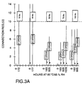
- FIG. 2A The environmental test results for the circuit assemblies of Example 1 testing are shown in Fig. 2A
- the penetration of the interconnected bumps and traces into the surface of the deformable substrate creates a circuit assembly with very uniform connection resistances as well as excellent connection stability, even when variations in bump height and trace thickness are considered. This uniformly good performance is observed at bonding pressures as low as 133 N.
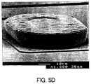
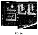
- Fig. 6A depicts the circuit traces on a substrate assembly made according to the invention, separated from the bumps on the 3M-D120X test chip, following the bonding procedure described in Example 1.
- Fig. 6B depicts the bumps on the 3M-D120X test chip, separated from the circuit traces on the substrate assembly, following the bonding procedure described in Example 1.
- the bonding conditions in Fig. 6 were: temperature 140 °C, force 267 N, time 20 seconds.
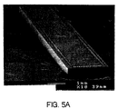
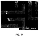
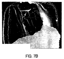
- Figs. 7A and 7B depict the circuit traces on a substrate assembly made according to the invention, separated from the bumps on the 3M-D120X test chip, following the bonding procedure described in Example 1 without the use of an adhesive.
- Figs. 7C and 7D depict the bumps on the 3M-D120X test chip, separated from the circuit traces on the substrate assembly, following the bonding procedure described in Example 1 without the use of an adhesive.
- gold/copper plating from circuit traces can be seen adhering to bump along with some PET (curled up).
- the bonding conditions in Fig. 7 were: temperature. 140 °C; force, 267 N; time, 20 seconds.
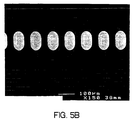
- Figs. 8A and 8B show the pulled-apart bond of Fig. 7 in which the sample has been rotated 70° from vertical.
- Fig. 8A shows the circuit side of the bond and 8B shows the bump (chip) side of the bond.
- the delamination of the metal circuit trace from the substrate surface is clearly visible. The delamination was caused by the force required to pull apart the bonded assembly.
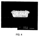
- Figs. 10A and 10B depict the pulled-apart bonds of Fig. 7A and 7C, respectively, at high magnification. These figures show that the pointed gold asperities on the bump which are present prior to the bonding procedure (see Fig. 4) become flattened during bonding. The cluster of small whitish spheres opposite the shadowed area in the shallow crater in Fig 10A are believed to be ductile fractures which may be evidence of fusion bonding between the gold bump and the gold surface of the circuit trace.
- Fig. 9A depicts the circuit traces on a substrate assembly made according to the invention, separated from the bumps on the 3M-D120X test chip, following the bonding procedure described in Example 1.
- Fig. 9B depicts the bumps on the 3M-D120X test chip, separated from the circuit traces on the substrate assembly made according to the present invention, following the bonding procedure described in Example 1.
- the dark areas are adhesive revealed by back-scattered electrons. The photographs in Fig. 9 dearly demonstrate that the adhesive is removed from the bump-trace interface during bonding to produce a highly reliable electrical connection.
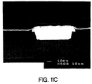
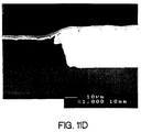
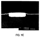
- Figs. 11A-F depict a cross-sectional view of a bump bonded to a circuit trace on a substrate assembly made according to the invention (substrate oriented at top of photo) prepared according to the procedure in Example 1 with increasing levels of bonding force.
- the "muffin-like" edges of the bump appear to be forced downward as increasing bonding pressure is applied.
- this edge has folded all the way down to the chip.
- Figs. 11A-F show that the gold-coated copper traces are bent over the edge and stretch in conformity to the periphery of the bump as the bump is deformed.
- the traces were probably bonded to the bumps at this point and part of the stretch (tensile strain) coincides with the deformation of the bumps.
- the softness of the bump and small radius of curvature at the bump edge therefore tend to spread out the strain induced in the traces over a larger area.
- Figs. 11A-F clearly show the collapse of the gold bump (from 40, to 36, to 34 and finally 24 ⁇ m thickness), thinning of adhesive film, and increasing depth of penetration of the PET film (from 0. to 4.5 to 7 and finally 8 ⁇ m) as bonding force is increased from 0 to 133 to 200 and then to 267 N (see Figs 11A, B; C, D; and E, F; respectively).
- Example 2 was the same as Example I except that the adhesive LT-1F was used. Ten (10) samples were prepared, aged, and monitored in the same manner as the samples of Example 1 As in Example 1, bond lines seemed to remain free of delamination in all samples over the course of the testing.
- the results of the environmental testing are shown in Fig. 2B.
- the results from Example 2 show more variability at lower bond forces than those of Example 1.
- the presence of the conductive particles did seem to prevent contact failures, even for a bond force of 67 Newtons
- the higher resistances measured in these examples were probably due to the high resistivity of the conductive particles.
- the conductive particles are plated to a level of 20% by weight. For a 5 ⁇ m diameter particle, this corresponds to a metal skin thickness of only about 1000 Angstroms. Therefore, the ohmic resistance of such a particle could be at least a few hundred milliohms At the higher bond forces, the occurrence of reduced connection resistances probably was an indication of an increasing level of direct contact between the bump and the circuit trace suppressing the effect of the particles.
- Example 3 was a comparative example to demonstrate the effectiveness of prior art bonding methods.
- Ten (10) samples were prepared by bonding 10 of the 3M-D120X test chips to ten of the ITO/glass test substrates using the LT-1U adhesive.
- the bonding method used was similar to that described in U.S. Patent No. 4,749,120 to Hatada.
- the curing condition was 140 °C for 20 seconds.
- Two samples were bonded at each of five different bond forces: 66.7, 133, 222, 334, and 445 N.
- the bonded samples were aged at 85 °C / 85 % relative humidity for a period of up to 1000 hrs, and were monitored periodically for interconnection resistance stability.
- Example 4 was the same as Example 3 except that the adhesive LT-1F was used. Ten (10) samples were prepared, aged. and monitored in the same manner as the samples of Example 3. The results of the environmental testing are shown in Fig. 3B.
- Example 4 show a marked improvement achieved by adding a small amount of the deformable conductive powder.
- the conductive powder appears to provide some accommodation of stress relaxation in the adhesive which is not provided by the bumps alone.
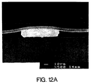
- This example demonstrates the effect of varying copper trace thickness, PET substrate thickness, and bonding temperature on penetration of the interconnected bumps and traces into the surface of the substrate.
- Samples were prepared using the standard bonding procedure described in Example 1.
- the adhesive used was a LT-1U film having a thickness of 25 ⁇ m.
- the substrate assembly was PET with a thickness of 25 or 50 ⁇ m which was plated with gold plated copper circuit traces having a thickness of 3 or 8 ⁇ m.
- the bonding conditions used were: bonding temperature 140 or 150 °C, bonding force 200 N, time 20 seconds.
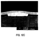
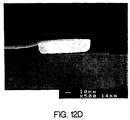
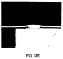
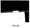
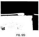
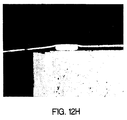
- Figs. 12A-12D (substrate oriented at top of photo) show scanning electron photomicrographs (500X) of cross-sections of the adhesively-bonded assemblies.
- Figs. 12E-12H depict optical photomicrographs (200X) of cross-sections corresponding to those of Figs. 12A-12D.
- the flex-circuits depicted in Fig. 12 have PET substrate thicknesses and copper circuit trace thicknesses as shown in Table I below Figure
- Figs. 12B, D, F, and H (3 ⁇ m copper traces on 50 and 25 ⁇ m PET, respectively) show sharp bending (high radius of curvature) of the circuit traces as they are bent around the periphery of the bump.
- Figs. 12A, C, F, and G (8 ⁇ m copper traces on 50 and 25 ⁇ m PET, respectively) show a gradual bending indicative of the greater stiffness of the thicker circuit trace.
- Fig. 12I is a scanning electron photomicrograph in backscatter mode (600X, substrate oriented at the top of photo) showing the wiping action that occurs as the edge of the bump deforms and stretches the circuit trace, thus enhancing the metal-to-metal contact between bump and circuit trace, thereby increasing the reliability of the pressure engaged electrical interconnection that is formed.
- This intimate electrical contact can be inferred by the brightness of the image at the edges of the bump and corresponding deformed trace due to the abundance of electron emission at the gold-to-gold interfaces involved.
- the dark areas in the center of the bump are believed to be due to residual amounts of trapped adhesive that was not squeezed out of the gap between the bump and corresponding circuit trace during the bonding process.
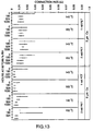
- the four probe connection resistance (range and mean) for each of the eight levels of the test matrix as a function of cumulative hours of environmental exposure is shown in Fig. 13.
- This example demonstrates how bump penetration varies with bond temperature.
- the samples were prepared using the standard bonding procedure described in Example 1.
- the substrate used was PET (thickness 25 ⁇ m) which was uniformly metallized on one major surface with electroplated copper (thickness 3 ⁇ m) which was overcoated with electroplated gold (thickness 750 nm).
- the adhesive film was omitted.
- the bonding conditions used were: temperature (40 - 160 °C in 10 °C increments), force (200 N), and time (20 seconds).
- test chips Thirteen (13) samples were prepared at each of the 13 bonding temperatures (total samples 169). None of the test chips were reused. After bonding, the test chips were removed, and the depth of bump penetration into the substrate was measured using a laser micrometer. Three widely-spaced points outside the perimeter formed by the bump impression were measured with micrometer to establish a reference plane (datum plane). The lowest point (maximum) depth in each depression was chosen as the penetration depth. The depth was measured in two depressions along each side of the chip (8 measurements per sample).
- the inter-metallic diffusion bonds formed between the bumps and circuit traces was sufficiently high to tear copper away from the PET at the bottom the bump impressions for bonding temperatures of 130 °C and higher.
Landscapes
- Wire Bonding (AREA)
- Laminated Bodies (AREA)
- Adhesives Or Adhesive Processes (AREA)
- Electric Connection Of Electric Components To Printed Circuits (AREA)
Applications Claiming Priority (3)
| Application Number | Priority Date | Filing Date | Title |
|---|---|---|---|
| US52113495A | 1995-08-29 | 1995-08-29 | |
| US521134 | 1995-08-29 | ||
| PCT/US1996/012606 WO1997008749A1 (en) | 1995-08-29 | 1996-08-01 | Deformable substrate assembly for adhesively bonded electronic device |
Publications (2)
| Publication Number | Publication Date |
|---|---|
| EP0847594A1 EP0847594A1 (en) | 1998-06-17 |
| EP0847594B1 true EP0847594B1 (en) | 2002-07-17 |
Family
ID=24075503
Family Applications (1)
| Application Number | Title | Priority Date | Filing Date |
|---|---|---|---|
| EP96926220A Expired - Lifetime EP0847594B1 (en) | 1995-08-29 | 1996-08-01 | Method of assembling an adhesively bonded electronic device using a deformable substrate |
Country Status (8)
| Country | Link |
|---|---|
| US (1) | US5714252A (enExample) |
| EP (1) | EP0847594B1 (enExample) |
| JP (1) | JPH11510649A (enExample) |
| KR (1) | KR19990044151A (enExample) |
| CN (1) | CN1194059A (enExample) |
| DE (1) | DE69622412T2 (enExample) |
| TW (1) | TW349269B (enExample) |
| WO (1) | WO1997008749A1 (enExample) |
Families Citing this family (45)
| Publication number | Priority date | Publication date | Assignee | Title |
|---|---|---|---|---|
| US5700398A (en) * | 1994-12-14 | 1997-12-23 | International Business Machines Corporation | Composition containing a polymer and conductive filler and use thereof |
| JPH1041694A (ja) * | 1996-07-25 | 1998-02-13 | Sharp Corp | 半導体素子の基板実装構造及びその実装方法 |
| JP3928753B2 (ja) | 1996-08-06 | 2007-06-13 | 日立化成工業株式会社 | マルチチップ実装法、および接着剤付チップの製造方法 |
| WO1998015593A1 (en) * | 1996-10-08 | 1998-04-16 | Fibercote Industries, Inc. | Sheet material for core support |
| JPH10270496A (ja) * | 1997-03-27 | 1998-10-09 | Hitachi Ltd | 電子装置、情報処理装置、半導体装置並びに半導体チップの実装方法 |
| DE69835747T2 (de) * | 1997-06-26 | 2007-09-13 | Hitachi Chemical Co., Ltd. | Substrat zur montage von halbleiterchips |
| US6297559B1 (en) | 1997-07-10 | 2001-10-02 | International Business Machines Corporation | Structure, materials, and applications of ball grid array interconnections |
| US6337522B1 (en) * | 1997-07-10 | 2002-01-08 | International Business Machines Corporation | Structure employing electrically conductive adhesives |
| US6120885A (en) | 1997-07-10 | 2000-09-19 | International Business Machines Corporation | Structure, materials, and methods for socketable ball grid |
| JP3625646B2 (ja) | 1998-03-23 | 2005-03-02 | 東レエンジニアリング株式会社 | フリップチップ実装方法 |
| JP3535746B2 (ja) * | 1998-08-20 | 2004-06-07 | ソニーケミカル株式会社 | フレキシブル基板製造方法 |
| US6840430B2 (en) * | 1998-07-30 | 2005-01-11 | Sony Chemicals, Corp. | Board pieces, flexible wiring boards and processes for manufacturing flexible wiring boards |
| US6100114A (en) * | 1998-08-10 | 2000-08-08 | International Business Machines Corporation | Encapsulation of solder bumps and solder connections |
| US6189208B1 (en) | 1998-09-11 | 2001-02-20 | Polymer Flip Chip Corp. | Flip chip mounting technique |
| US6535393B2 (en) * | 1998-12-04 | 2003-03-18 | Micron Technology, Inc. | Electrical device allowing for increased device densities |
| US6274224B1 (en) | 1999-02-01 | 2001-08-14 | 3M Innovative Properties Company | Passive electrical article, circuit articles thereof, and circuit articles comprising a passive electrical article |
| US6410415B1 (en) | 1999-03-23 | 2002-06-25 | Polymer Flip Chip Corporation | Flip chip mounting technique |
| JP2001031929A (ja) * | 1999-07-21 | 2001-02-06 | Sony Chem Corp | 接続構造体 |
| TW511122B (en) * | 1999-12-10 | 2002-11-21 | Ebara Corp | Method for mounting semiconductor device and structure thereof |
| US20030009876A1 (en) * | 2000-01-14 | 2003-01-16 | Akira Yamauchi | Method and device for chip mounting |
| WO2001056340A1 (en) * | 2000-01-28 | 2001-08-02 | Sony Chemicals Corp. | Substrate material piece, flexible circuit board, and method of manufacturing the flexible circuit board |
| US6584670B2 (en) * | 2000-02-21 | 2003-07-01 | Larry J. Costa | Electrical terminal implementation device |
| DE60141391D1 (de) * | 2000-03-10 | 2010-04-08 | Chippac Inc | Flipchip-Verbindungsstruktur und dessen Herstellungsverfahren |
| US10388626B2 (en) * | 2000-03-10 | 2019-08-20 | STATS ChipPAC Pte. Ltd. | Semiconductor device and method of forming flipchip interconnect structure |
| DE10014300A1 (de) * | 2000-03-23 | 2001-10-04 | Infineon Technologies Ag | Halbleiterbauelement und Verfahren zu dessen Herstellung |
| US6423905B1 (en) * | 2000-05-01 | 2002-07-23 | International Business Machines Corporation | Printed wiring board with improved plated through hole fatigue life |
| US6512183B2 (en) * | 2000-10-10 | 2003-01-28 | Matsushita Electric Industrial Co., Ltd. | Electronic component mounted member and repair method thereof |
| EP1360715A2 (de) * | 2001-02-13 | 2003-11-12 | Pac Tech - Packaging Technologies GmbH | Presskontaktierung von mikrochips |
| EP1393368A2 (en) * | 2001-05-17 | 2004-03-03 | Koninklijke Philips Electronics N.V. | Product comprising a substrate and a chip attached to the substrate |
| DE10124770C1 (de) * | 2001-05-21 | 2002-10-17 | Infineon Technologies Ag | Verfahren zur Kontaktierung eines elektrischen Bauelementes mit einem eine Leiterstruktur aufweisenden Substrat |
| US6871395B2 (en) * | 2001-08-06 | 2005-03-29 | Siemens Technology-To-Business Center, Llc. | Methods for manufacturing a tactile sensor using an electrically conductive elastomer |
| JP4159778B2 (ja) * | 2001-12-27 | 2008-10-01 | 三菱電機株式会社 | Icパッケージ、光送信器及び光受信器 |
| JP4045838B2 (ja) * | 2002-04-12 | 2008-02-13 | 松下電器産業株式会社 | 部品装着管理方法 |
| JP2004119430A (ja) * | 2002-09-24 | 2004-04-15 | Tadatomo Suga | 接合装置および方法 |
| US7176044B2 (en) * | 2002-11-25 | 2007-02-13 | Henkel Corporation | B-stageable die attach adhesives |
| TWI228286B (en) * | 2003-11-24 | 2005-02-21 | Ind Tech Res Inst | Bonding structure with buffer layer and method of forming the same |
| FR2875995B1 (fr) * | 2004-09-24 | 2014-10-24 | Oberthur Card Syst Sa | Procede de montage d'un composant electronique sur un support, de preference mou, et entite electronique ainsi obtenue, telle q'un passeport |
| KR100757910B1 (ko) * | 2006-07-06 | 2007-09-11 | 삼성전기주식회사 | 매립패턴기판 및 그 제조방법 |
| US8201325B2 (en) * | 2007-11-22 | 2012-06-19 | International Business Machines Corporation | Method for producing an integrated device |
| JP5528169B2 (ja) * | 2010-03-26 | 2014-06-25 | 東洋ゴム工業株式会社 | 研磨パッドおよびその製造方法、ならびに半導体デバイスの製造方法 |
| US9472131B2 (en) * | 2012-11-02 | 2016-10-18 | Apple Inc. | Testing of integrated circuit to substrate joints |
| JP6380069B2 (ja) * | 2014-12-11 | 2018-08-29 | 住友電気工業株式会社 | 光送信モジュール |
| TWI696300B (zh) | 2016-03-15 | 2020-06-11 | 晶元光電股份有限公司 | 半導體裝置及其製造方法 |
| TWI581417B (zh) * | 2016-04-11 | 2017-05-01 | 友達光電股份有限公司 | 發光裝置及其製造方法 |
| TW202541302A (zh) * | 2019-02-04 | 2025-10-16 | 日商索尼半導體解決方案公司 | 電子裝置 |
Family Cites Families (11)
| Publication number | Priority date | Publication date | Assignee | Title |
|---|---|---|---|---|
| DE2610539A1 (de) * | 1976-03-12 | 1977-09-22 | Siemens Ag | Halbleiterbauelement mit elektrischen kontakten und verfahren zur herstellung solcher kontakte |
| JPS59195837A (ja) * | 1983-04-21 | 1984-11-07 | Sharp Corp | Lsiチツプボンデイング方法 |
| US4643935A (en) * | 1986-01-21 | 1987-02-17 | Burroughs Corporation | Epoxy-glass integrated circuit package having bonding pads in a stepped cavity |
| US4749120A (en) * | 1986-12-18 | 1988-06-07 | Matsushita Electric Industrial Co., Ltd. | Method of connecting a semiconductor device to a wiring board |
| EP0337445A3 (en) * | 1988-04-13 | 1991-01-16 | Hitachi, Ltd. | Laminar structure comprising organic material and inorganic material, methods for producing it and its use |
| US5001542A (en) * | 1988-12-05 | 1991-03-19 | Hitachi Chemical Company | Composition for circuit connection, method for connection using the same, and connected structure of semiconductor chips |
| US5074947A (en) * | 1989-12-18 | 1991-12-24 | Epoxy Technology, Inc. | Flip chip technology using electrically conductive polymers and dielectrics |
| US5121190A (en) * | 1990-03-14 | 1992-06-09 | International Business Machines Corp. | Solder interconnection structure on organic substrates |
| US5270260A (en) * | 1990-08-23 | 1993-12-14 | Siemens Aktiengesellschaft | Method and apparatus for connecting a semiconductor chip to a carrier system |
| US5261156A (en) * | 1991-02-28 | 1993-11-16 | Semiconductor Energy Laboratory Co., Ltd. | Method of electrically connecting an integrated circuit to an electric device |
| US5258577A (en) * | 1991-11-22 | 1993-11-02 | Clements James R | Die mounting with uniaxial conductive adhesive |
-
1996
- 1996-08-01 CN CN96196568A patent/CN1194059A/zh active Pending
- 1996-08-01 EP EP96926220A patent/EP0847594B1/en not_active Expired - Lifetime
- 1996-08-01 KR KR1019980701384A patent/KR19990044151A/ko not_active Withdrawn
- 1996-08-01 WO PCT/US1996/012606 patent/WO1997008749A1/en not_active Ceased
- 1996-08-01 DE DE69622412T patent/DE69622412T2/de not_active Expired - Fee Related
- 1996-08-01 JP JP8536019A patent/JPH11510649A/ja active Pending
- 1996-08-15 TW TW085109945A patent/TW349269B/zh active
-
1997
- 1997-01-02 US US08/778,112 patent/US5714252A/en not_active Expired - Lifetime
Also Published As
| Publication number | Publication date |
|---|---|
| WO1997008749A1 (en) | 1997-03-06 |
| TW349269B (en) | 1999-01-01 |
| JPH11510649A (ja) | 1999-09-14 |
| CN1194059A (zh) | 1998-09-23 |
| US5714252A (en) | 1998-02-03 |
| DE69622412D1 (de) | 2002-08-22 |
| EP0847594A1 (en) | 1998-06-17 |
| KR19990044151A (ko) | 1999-06-25 |
| HK1012521A1 (en) | 1999-08-06 |
| DE69622412T2 (de) | 2003-03-20 |
Similar Documents
| Publication | Publication Date | Title |
|---|---|---|
| EP0847594B1 (en) | Method of assembling an adhesively bonded electronic device using a deformable substrate | |
| Kristiansen et al. | Overview of conductive adhesive interconnection technologies for LCDs | |
| JP2586154B2 (ja) | 回路接続用組成物及びこれを用いた接続方法並びに半導体チップの接続構造 | |
| JP7517384B2 (ja) | 異方性導電フィルム及びその製造方法、並びに接続構造体及びその製造方法 | |
| US5783465A (en) | Compliant bump technology | |
| US6919642B2 (en) | Method for bonding IC chips to substrates incorporating dummy bumps and non-conductive adhesive and structures formed | |
| US6046910A (en) | Microelectronic assembly having slidable contacts and method for manufacturing the assembly | |
| KR100384314B1 (ko) | 회로기판에의 전자부품 실장방법 및 장치 | |
| Yim et al. | Anisotropic conductive films (ACFs) for ultra-fine pitch chip-on-glass (COG) applications | |
| US7901768B2 (en) | Multilayer anisotropic conductive adhesive and connection structure using the same | |
| US20080185705A1 (en) | Microelectronic packages and methods therefor | |
| US20050218517A1 (en) | Semiconductor flip-chip package and method for the fabrication thereof | |
| KR101150613B1 (ko) | 접착 필름, 접속 방법 및 접합체 | |
| JPH09312176A (ja) | 接続部材および該接続部材を用いた電極の接続構造並びに接続方法 | |
| KR20120060923A (ko) | 접착 필름, 접속 방법 및 접합체 | |
| US6605491B1 (en) | Method for bonding IC chips to substrates with non-conductive adhesive | |
| JPH08279371A (ja) | 接続部材および該接続部材を用いた電極の接続構造並びに接続方法 | |
| JP7697292B2 (ja) | はんだバンプ形成装置 | |
| Aschenbrenner et al. | Adhesive flip chip bonding on flexible substrates | |
| KR20120022580A (ko) | 실장체의 제조 방법, 접속 방법 및 이방성 도전막 | |
| JPH05258830A (ja) | 回路の接続方法 | |
| HK1012521B (en) | Method of assembling an adhesively bonded electronic device using a deformable substrate | |
| JP2004006417A (ja) | 接続部材及びこれを用いた電極の接続構造 | |
| JP4045471B2 (ja) | 電子部品実装法 | |
| JP4223581B2 (ja) | マルチチップ実装法 |
Legal Events
| Date | Code | Title | Description |
|---|---|---|---|
| PUAI | Public reference made under article 153(3) epc to a published international application that has entered the european phase |
Free format text: ORIGINAL CODE: 0009012 |
|
| 17P | Request for examination filed |
Effective date: 19980130 |
|
| AK | Designated contracting states |
Kind code of ref document: A1 Designated state(s): DE FR GB IT NL |
|
| 17Q | First examination report despatched |
Effective date: 19990818 |
|
| RTI1 | Title (correction) |
Free format text: METHOD OF ASSEMBLING AN ADHESIVELY BONDED ELECTRONIC DEVICE USING A DEFORMABLE SUBSTRATE |
|
| GRAG | Despatch of communication of intention to grant |
Free format text: ORIGINAL CODE: EPIDOS AGRA |
|
| RTI1 | Title (correction) |
Free format text: METHOD OF ASSEMBLING AN ADHESIVELY BONDED ELECTRONIC DEVICE USING A DEFORMABLE SUBSTRATE |
|
| GRAG | Despatch of communication of intention to grant |
Free format text: ORIGINAL CODE: EPIDOS AGRA |
|
| GRAH | Despatch of communication of intention to grant a patent |
Free format text: ORIGINAL CODE: EPIDOS IGRA |
|
| GRAH | Despatch of communication of intention to grant a patent |
Free format text: ORIGINAL CODE: EPIDOS IGRA |
|
| GRAA | (expected) grant |
Free format text: ORIGINAL CODE: 0009210 |
|
| AK | Designated contracting states |
Kind code of ref document: B1 Designated state(s): DE FR GB IT NL |
|
| PG25 | Lapsed in a contracting state [announced via postgrant information from national office to epo] |
Ref country code: NL Free format text: LAPSE BECAUSE OF FAILURE TO SUBMIT A TRANSLATION OF THE DESCRIPTION OR TO PAY THE FEE WITHIN THE PRESCRIBED TIME-LIMIT Effective date: 20020717 Ref country code: IT Free format text: LAPSE BECAUSE OF FAILURE TO SUBMIT A TRANSLATION OF THE DESCRIPTION OR TO PAY THE FEE WITHIN THE PRE;WARNING: LAPSES OF ITALIAN PATENTS WITH EFFECTIVE DATE BEFORE 2007 MAY HAVE OCCURRED AT ANY TIME BEFORE 2007. THE CORRECT EFFECTIVE DATE MAY BE DIFFERENT FROM THE ONE RECORDED.SCRIBED TIME-LIMIT Effective date: 20020717 Ref country code: FR Free format text: LAPSE BECAUSE OF FAILURE TO SUBMIT A TRANSLATION OF THE DESCRIPTION OR TO PAY THE FEE WITHIN THE PRESCRIBED TIME-LIMIT Effective date: 20020717 |
|
| REG | Reference to a national code |
Ref country code: GB Ref legal event code: FG4D |
|
| REF | Corresponds to: |
Ref document number: 69622412 Country of ref document: DE Date of ref document: 20020822 |
|
| PG25 | Lapsed in a contracting state [announced via postgrant information from national office to epo] |
Ref country code: GB Free format text: LAPSE BECAUSE OF NON-PAYMENT OF DUE FEES Effective date: 20021017 |
|
| NLV1 | Nl: lapsed or annulled due to failure to fulfill the requirements of art. 29p and 29m of the patents act | ||
| EN | Fr: translation not filed | ||
| PLBE | No opposition filed within time limit |
Free format text: ORIGINAL CODE: 0009261 |
|
| STAA | Information on the status of an ep patent application or granted ep patent |
Free format text: STATUS: NO OPPOSITION FILED WITHIN TIME LIMIT |
|
| GBPC | Gb: european patent ceased through non-payment of renewal fee |
Effective date: 20021017 |
|
| 26N | No opposition filed |
Effective date: 20030422 |
|
| PGFP | Annual fee paid to national office [announced via postgrant information from national office to epo] |
Ref country code: DE Payment date: 20080930 Year of fee payment: 13 |
|
| PG25 | Lapsed in a contracting state [announced via postgrant information from national office to epo] |
Ref country code: DE Free format text: LAPSE BECAUSE OF NON-PAYMENT OF DUE FEES Effective date: 20100302 |