EP0843300A2 - Graustufenansteuervorrichtung für eine passive Flüssigkristall-Anzeige - Google Patents
Graustufenansteuervorrichtung für eine passive Flüssigkristall-Anzeige Download PDFInfo
- Publication number
- EP0843300A2 EP0843300A2 EP97119894A EP97119894A EP0843300A2 EP 0843300 A2 EP0843300 A2 EP 0843300A2 EP 97119894 A EP97119894 A EP 97119894A EP 97119894 A EP97119894 A EP 97119894A EP 0843300 A2 EP0843300 A2 EP 0843300A2
- Authority
- EP
- European Patent Office
- Prior art keywords
- gray scale
- liquid crystal
- data
- display
- frame
- Prior art date
- Legal status (The legal status is an assumption and is not a legal conclusion. Google has not performed a legal analysis and makes no representation as to the accuracy of the status listed.)
- Granted
Links
Images


Classifications
-
- G—PHYSICS
- G09—EDUCATION; CRYPTOGRAPHY; DISPLAY; ADVERTISING; SEALS
- G09G—ARRANGEMENTS OR CIRCUITS FOR CONTROL OF INDICATING DEVICES USING STATIC MEANS TO PRESENT VARIABLE INFORMATION
- G09G3/00—Control arrangements or circuits, of interest only in connection with visual indicators other than cathode-ray tubes
- G09G3/20—Control arrangements or circuits, of interest only in connection with visual indicators other than cathode-ray tubes for presentation of an assembly of a number of characters, e.g. a page, by composing the assembly by combination of individual elements arranged in a matrix no fixed position being assigned to or needed to be assigned to the individual characters or partial characters
- G09G3/34—Control arrangements or circuits, of interest only in connection with visual indicators other than cathode-ray tubes for presentation of an assembly of a number of characters, e.g. a page, by composing the assembly by combination of individual elements arranged in a matrix no fixed position being assigned to or needed to be assigned to the individual characters or partial characters by control of light from an independent source
- G09G3/36—Control arrangements or circuits, of interest only in connection with visual indicators other than cathode-ray tubes for presentation of an assembly of a number of characters, e.g. a page, by composing the assembly by combination of individual elements arranged in a matrix no fixed position being assigned to or needed to be assigned to the individual characters or partial characters by control of light from an independent source using liquid crystals
- G09G3/3611—Control of matrices with row and column drivers
- G09G3/3622—Control of matrices with row and column drivers using a passive matrix
-
- G—PHYSICS
- G09—EDUCATION; CRYPTOGRAPHY; DISPLAY; ADVERTISING; SEALS
- G09G—ARRANGEMENTS OR CIRCUITS FOR CONTROL OF INDICATING DEVICES USING STATIC MEANS TO PRESENT VARIABLE INFORMATION
- G09G3/00—Control arrangements or circuits, of interest only in connection with visual indicators other than cathode-ray tubes
- G09G3/20—Control arrangements or circuits, of interest only in connection with visual indicators other than cathode-ray tubes for presentation of an assembly of a number of characters, e.g. a page, by composing the assembly by combination of individual elements arranged in a matrix no fixed position being assigned to or needed to be assigned to the individual characters or partial characters
- G09G3/2007—Display of intermediate tones
- G09G3/2018—Display of intermediate tones by time modulation using two or more time intervals
-
- G—PHYSICS
- G09—EDUCATION; CRYPTOGRAPHY; DISPLAY; ADVERTISING; SEALS
- G09G—ARRANGEMENTS OR CIRCUITS FOR CONTROL OF INDICATING DEVICES USING STATIC MEANS TO PRESENT VARIABLE INFORMATION
- G09G3/00—Control arrangements or circuits, of interest only in connection with visual indicators other than cathode-ray tubes
- G09G3/20—Control arrangements or circuits, of interest only in connection with visual indicators other than cathode-ray tubes for presentation of an assembly of a number of characters, e.g. a page, by composing the assembly by combination of individual elements arranged in a matrix no fixed position being assigned to or needed to be assigned to the individual characters or partial characters
- G09G3/2007—Display of intermediate tones
- G09G3/2044—Display of intermediate tones using dithering
- G09G3/2051—Display of intermediate tones using dithering with use of a spatial dither pattern
- G09G3/2055—Display of intermediate tones using dithering with use of a spatial dither pattern the pattern being varied in time
Definitions
- the present invention relates to a liquid crystal display unit and more particularly to a liquid crystal display unit of a passive matrix type including pixels each formed at each intersecting point of scanning electrodes and data electrodes disposed orthogonally to each other and having the transmission factor which is varied in accordance with an average of squared difference between voltages applied to the scanning electrodes and the data electrodes. Further, the present invention relates to a liquid crystal controller capable of driving the liquid crystal display unit of the passive matrix type at a low cost and with high display quality.
- a driving frame frequency for obtaining the optimum contrast in an STN liquid crystal is different depending on a response speed of liquid crystal material. It is known that the frequency is 90 to 120 Hz for the response time of 300 ms and 160 to 240 Hz for 100 ms. The frequency is higher as compared with a frame frequency of 60 to 70 Hz used in a CRT or a TFT liquid crystal. For example, in order to convert a signal having the frame frequency into a display signal for the STN liquid crystal, it is necessary that a frame memory for storing display data is used to convert the frame frequency.
- a driving method of assigning binary information of display on or off to one pixel is used mainly. Accordingly, in order to display gray scale data, that is, data other than the display on or off in one pixel, any special processing is required. As measures for realizing this processing, there is a frame rate control (FRC) system.
- FRC frame rate control
- the FRC system several frames are defined as one period and a rate of the display on or off in the period is set to attain the gray scale.
- FRC pattern a pattern composed of the display on and off in a matrix having a certain size is formed and the FRC pattern is switched for each frame.
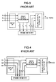
- the liquid crystal controller performs the frame frequency conversion and the gray scale processing in accordance with a method as shown in Fig. 3 in which the gray scale processing is first performed and then display data are stored in the frame memory to convert the frame frequency or another method as shown in Fig. 4 in which gray scale data are all stored in the frame memory to convert the frame frequency and then the gray scale processing is performed.
- a controller as shown in Fig. 3 is disclosed in, for example, SID '96 Digest, pp. 356 issued by the Society for Information Display and such a controller as shown in Fig. 4 is disclosed in, for example, a data sheet, pp. 98 of a liquid crystal controller 7548 issued by Cirrus Logic Corporation.
- the inputted frame frequency of 60 to 75 Hz is used as the switching frequency of the FRC pattern as it is. Accordingly, there is a problem that the switching of the FRC pattern is apt to be seen and recognized. More particularly, it seems that gray scale display portions are moved or flicker.
- the switching frequency of the FRC pattern is the same as the frame frequency of an output of the liquid crystal and is high to some degree. Accordingly, the pattern movement of the gray scale display portions are reduced.
- it is necessary to store all of the display data including the gray scale information of several bits per pixel into a frame memory there is a problem that the frame memory capacity increases.
- a liquid crystal control method of the present invention includes a preceding stage for gray scale processing performed before written in the frame memory and a latter stage for gray scale processing performed after conversion of the frequency and reading.
- a liquid crystal controller of the present invention includes gray scale processors for performing the FRC system and disposed before and after the frame memory. Several bits of n-bit gray scale data inputted to the gray scale processors are subjected to the gray scale processing before written in the frame memory and remaining several bits are subjected to the gray scale processing after read from the frame memory. Display signals obtained by both the gray scale processors are combined to be converted into an output display data of one bit.
- the present invention includes not only the liquid crystal controller but also a liquid crystal monitor as shown in Fig. 12.
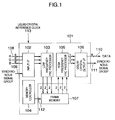
- Fig. 1 is a block diagram schematically illustrating a liquid crystal controller according to a first embodiment of the present invention.
- numeral 101 denotes a liquid crystal controller of the present invention.
- numeral 102 denotes an input interface unit
- 103 a gray scale processor provided before a frame memory and which is referred to as a low frequency FRC processor
- 104 a memory controller
- 105 a gray scale processor provided after the frame memory and which is hereinafter referred to as a high frequency FRC processor
- 106 a liquid crystal interface unit
- 107 a general-purpose frame memory
- 108 an input display data group
- 109 a synchronizing signal group for the input display data.
- the input display data group 108 and the synchronizing signal group 109 are input signals to the liquid crystal controller.
- Numeral 110 denotes an output display data group and 111 a synchronizing signal group for the input display data.
- the output display data group 110 and the synchronizing signal group 111 are output signals of the liquid crystal controller 101.
- Numeral 112 denotes a memory control signal group which controls writing and reading of display data to the frame memory, and 113 a liquid crystal reference clock, which is an original signal for the synchronizing signal group 111 of the output display data and the data reading signal from the main frame 107.
- the display data 108 to be inputted and the synchronising signal 109 are subjected to adjustment or conversion of the timing thereof used when the data and the signal are supplied to each block.
- the display data 108 are separated into R (red), G (green) and B (blue) data, each composed of gray scale data of 6 bits.
- the input synchronizing signal group 109 includes a clock signal synchronized with the input display data, a signal indicative of switching of a horizontal period, a signal indicative of switching of a frame period, and a signal indicative of an effective time of the display data.
- These signals conform to, for example, CL2, CL1, FLM and DPTMG signals described in Hitachi LCD controller/driver LSI data book, pp. 1186-1193, "HD66330T (TFT Driver)" issued by Hitachi, Ltd. and the input display data and the mutual timing relation thereof conform to contents described in the same data book.
- the low frequency FRC processor 103 In the low frequency FRC processor 103, lower 5 bits of each of the 6-bit input display data 108 are subjected to FRC processing to be converted into one-bit display data. The most significant bit thereof is not processed. That is, the 6-bit input display data 108 is produced to the frame memory 107 as 2-bit display data.
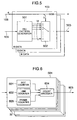
- the low frequency FRC processor 103 includes, as shown in Fig. 5, an FRC pattern generator 501 and an FRC pattern selector 502.
- the FRC pattern generator 501 generates FRC patterns of 32 kinds corresponding to lower 5 bits of the input data.
- the FRC pattern selector 502 selects the FRC pattern of 32 kinds generated by the FRC pattern generator 501, in accordance with lower 5 bits of the input display data 108 and produces the selected FRC pattern as a low frequency selection FRC signal 503.
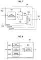
- the FRC pattern generator 501 includes, as shown in Fig. 6, a dot counter 601, a line counter 602, a frame counter 603 and a count encoder 604. Clocks of the counters 601 to 603 are CL2, CL1 and FLM, respectively, or close resemblances thereto, and periods of the counters 601 to 603 correspond to periods in the horizontal direction, the vertical direction and the frame direction of the FRC pattern, respectively.
- the count encoder 604 generates a signal corresponding to the display on or off in accordance with counts of the counters 601 to 603 and produces an FRC pattern signal group 605.
- the combination order of the display on and off in the FRC pattern deeply concerns the display quality of the STN liquid crystal. Accordingly, the way of thinking and an example of a definite FRC pattern for ameliorating the display quality will be described later.
- the memory controller 104 produces the memory control signal group 112 from the synchronizing signal group 109 and the liquid crystal reference clock 113.
- the memory control signal group 112 conforms to the specification of the used frame memory and when HM5241605 described in pp. 858-887 of the IC memory data book issued by Hitachi, Ltd., for example, is used as the frame memory, the frame memory produces the memory control signal group 112 conforming to the memory control signal group described in the data book.
- a writing control signal group to the frame memory 107 is produced in synchronism with the CL2 of the input synchronizing signal group 109 and a reading control signal group from the frame memory 107 is produced in synchronism with the liquid crystal reference clock 113.
- the high frequency FRC processor 105 includes, as shown in Fig. 7, an FRC pattern generator 701, an FRC pattern selector 702 and an FRC pattern mixer 703.
- the FRC pattern generator 701 generates FRC patterns of two kinds corresponding to display data 704 of the most significant bit read from the frame memory 107.
- the FRC pattern selector 702 selects the FRC pattern of two kinds generated by the FRC pattern generator 701 in accordance with a value of the most significant bit of the display data 704 and produces it as a high frequency selection FRC signal 706.
- the FRC pattern mixer 703 takes a logical AND of the high frequency selection FRC signal 706 and the low frequency selection FRC signal 705 read from the frame memory 107 and produces it as a gray scale processing signal 707.
- the FRC pattern generator 701 includes, as shown in Fig. 8, a dot counter 801, a line counter 802, a frame counter 803 and a counter encoder 804.
- Clocks of the counters 801 to 803 are liquid crystal output synchronizing signals CL2, CL1 and FLM described later, respectively, or close resemblances thereto.
- the respective periods of the clocks of the counters 801 to 802 are all 2 and correspond to the periods in the horizontal direction, the vertical direction and the frame direction of the FRC pattern.
- the counter encoder 804 produces a signal corresponding to the display on and off in accordance with counts of the counters 801 to 803 and generates an FRC pattern.
- the FRC pattern is a checker-board pattern of two by two pixels constituting a unit matrix and includes one half portion in which display on or off data is displayed and the other half portion in which the low frequency selection FRC signal 705 is displayed as it is. Further, locations of these portions are switched one after the other for each frame.
- the liquid crystal interface unit 106 converts the gray scale processing signals 707 for R, G and B data of each one bit converted by the high frequency FRC processing unit 105 to produce the output display data group 110. Further, the liquid crystal interface unit 106 produces the output synchronizing signal group 111 from the liquid crystal reference clock 113. In the embodiment, the output display data group 110 are assumed to be produced in the form of 8 pixels in parallel. In addition, the output synchronizing signal group 111 conforms to CL2, CL1, FLM and DISPOFF described in Hitachi LCD controller/driver LSI data book, pp. 737-750 issued by Hitachi, Ltd., for example, and the output display data 110 and the mutual timing relation conform to description of the data book.
- Fig. 10 The flow of the gray scale processing of the display data in the first embodiment of the present invention as described above is shown in Fig. 10 collectively.
- the gray scale data when the gray scale data of 6 bits to be inputted is written in the frame memory, the gray scale data is reduced to two bits and accordingly the capacity of the frame memory can be reduced.
- the switching frequency of the FRC pattern is the same as the frame frequency of the produced liquid crystal output signal and accordingly pattern movement in the gray scale display portion can be reduced.
- the output frame frequency is an integral multiple of the input frame frequency. This reason is that the completion period of the mixed FRC pattern in the frame direction is short and pattern movement in the gray scale display portion can be more reduced.
- the output data of the liquid crystal is supposed to have 8 parallel pixels, while the present invention is not limited thereto and for example the picture data may be divided into upper picture data and lower picture data to be outputted. In this case, when two planes for upper picture and lower picture are provided as the frame memory, control thereof is easy.
- the most significant bit of the input data is set to be the selection signal of the high frequency FRC pattern, while the selection signal is not limited thereto and the upper 2 bits of the input data may be used as the selection signal of the high frequency FRC pattern.
- the display data written in the frame memory includes three bits per pixel, while the frame memory is required to have the capacity sufficient to store the display data of three bits per pixel.
- display can be changed for each frame even if the frame memory is not provided for the capacity of the display data.
- the change for each frame means that the display for the N-th frame is different from the display for the (N+1)-th frame in the display example shown in Fig. 2.
- the frame memory must be provided for the capacity of the display data.
- the same display is repeated twice or more.
- the display data is the gray scale data separated into R (red), G (green) and B (blue) data each 6 bits.
- the frame memory in the first embodiment of the present invention is provided in the liquid crystal controller.
- Fig. 11 is a schematic diagram illustrating the second embodiment.
- Numeral 1101 denotes a liquid crystal controller of the present invention and 1102 a frame memory.
- Other blocks and signal groups are the same as those of the liquid crystal controller of the first embodiment and perform the same operation. Accordingly, detailed description of operation of the embodiment is omitted. Since the second embodiment of the present invention can be realized by one-chip LSI including the frame memory, the high-speed circuit operation and the low-cost system configuration can be attained.
- the second embodiment can attain the same effects as in the first embodiment.
- the liquid crystal controller in the first and second embodiments of the present invention is included in a liquid crystal module.
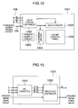
- Fig. 12 is a schematic diagram illustrating the third embodiment.
- Numeral 1201 denotes a liquid crystal module and 1202 a liquid crystal controller, which is the same as that in the first and second embodiments of the present invention.
- Numeral 1203 denotes a data driver, which can be realized by means of a liquid crystal driver described in Hitachi LCD controller/driver LSI data book, pp. 737-750 issued by Hitachi, Ltd., for example.
- Numeral 1204 denotes a scanning driver, which can be realized by means of a liquid crystal driver described in Hitachi LCD controller/driver LSI data book, pp.
- Numeral 1205 denotes a power supply circuit, which produces a power supply voltage required in the data driver 1203 and the scanning driver 1204.
- Numeral 1206 denotes a liquid crystal panel of the passive matrix type.
- the input signals of the liquid crystal module 1201 of the present invention are the same as the input signals of the liquid crystal controller of the first and second embodiments of the present invention and inputted to the liquid crystal controller 1202. Further, the output signals of the liquid crystal control 1202 are the same as the output signals of the liquid crystal controller of the first and second embodiment of the present invention and supplied to the data driver 1203 and the scanning driver 1204.
- the liquid crystal controller since the liquid crystal controller is included in the liquid crystal module, the digital data for R, G and B data each being 6 bits, for example, can be made to the input signals. Since the digital data for R, G and B data each being 6 bits are originally the input signals of the TFT liquid crystal module, the liquid crystal module of the third embodiment of the present invention can include the interchangeability of the interface to the TFT liquid crystal module.
- Fig. 13 is a schematic diagram illustrating the fourth embodiment.
- Numeral 1301 denotes a liquid crystal controller of the present invention, 1302 a scale processing controller, and 1303 an A/D converter.
- the scale processing controller 1302 is the same as the liquid crystal controller in the first and second embodiments of the present invention.
- the A/D converter 1303 can be realized by means of CXA3086Q described in A/D converter data book pp. 1-8 issued by Sony, for example.
- the input of the A/D converter has the interchangeability with CRT and the output thereof has the interchangeability with the TFT liquid crystal module. That is, by using the liquid crystal display controller of the fourth embodiment of the present invention, the STN liquid crystal display unit having the interchangeability of interface to the CRT can be realized.
- the fifth embodiment of the present invention describes the way of thinking of the FRC pattern and a definite example for ameliorating the display quality for the liquid crystal controller of the present invention.
- Figs. 14 and 15 show FRC patterns and liquid crystal applied voltage waveforms when the FRC patterns are displayed.
- the changes cause distortion of the scanning voltage waveform by means of a capacitance component of the liquid crystal and a resistance component of the electrodes. Since the distortion of the scanning voltage waveform changes an effective value of the liquid crystal applied voltage, cross-talk named shadowing is apt to be produced.
- the changing directions of the data voltages are opposite on halves. In this case, distortion of the scanning voltage waveform is canceled each other and is hardly produced. Accordingly, in this case, the shadowing can be reduced.
- the condition that the changing directions of the data voltages are opposite on halves is considered the condition shown in Fig. 15.
- the low frequency FRC pattern and the high frequency FRC pattern are combined to be displayed. Accordingly, it is required that the combined FRC pattern satisfies the above condition.
- This condition is described with reference to Figs. 16 and 17.
- the low frequency FRC pattern is constituted by a matrix of 4x4 pixels and in Fig.
- the low frequency FRC pattern is constituted by a matrix of 3x3 pixels.
- the high frequency pattern is the checker-board pattern of 2x2 pixels in the same manner as the first to fourth embodiments of the present invention.
- the low frequency FRC pattern in Figs. 16 and 17 satisfies the above-described condition that the rate of the display on and off in the FRC pattern matrix is constant on any scanning line.
- the matrix of the combined FRC pattern is composed of 4x4 pixels.
- the rate of the display on and off in the FRC pattern matrix is different depending on the scanning line. Accordingly, in the case of Fig. 16, since the distortion occurs in the scanning voltage waveform as described above, the shadowing is apt to be produced. On the contrary, in the FRC pattern of Fig. 17, since the size (period) of the matrix of the combined FRC pattern is the least common multiple of the sizes of the matrixes of the low frequency FRC pattern and the high frequency FRC pattern, the matrix of the combined FRC pattern is composed of 6x6 pixels. At this time, the rate of the display on and off in the FRC pattern matrix is 5 to 1 (5:1) irrespective of the scanning line. Accordingly, in the case of Fig.
- the shadowing can be reduced.
- the rate of the display on and off in the FRC pattern matrix is constant on any scanning line.
- the condition is that the number of pixels in the direction of the scanning line of the matrix of the low frequency FRC pattern is made odd when the high frequency FRC pattern is the checker-board pattern.
- the condition of the FRC pattern for ameliorating the display quality can be expressed from the above consideration by the definition that the rate of the display on and off in the low frequency FRC pattern matrix is constant on any scanning line and the number of pixels in the direction of the scanning line of the matrix of the low frequency FRC pattern is odd.
- the high frequency FRC pattern is set to be the checker-board pattern of 2x2 pixels, while the present invention is not limited thereto and as far as the condition that the rate of the display on and off in the combined FRC pattern matrix is constant on any scanning line is satisfied, any pattern may be used.
- the combined FRC pattern of the condition described in the fifth embodiment of the present invention can be used to attain the gray scale display with high quality in which occurrence of shadowing is suppressed. It is desirable that the combined FRC pattern of the condition described in the fifth embodiment of the present invention is applied to the liquid crystal controller of the first to fourth embodiments of the present invention.
- the controller of the liquid crystal display of the passive matrix type in which pixels are formed at the intersecting points of the scanning electrodes and the data electrodes disposed orthogonally to each other and the pixels have the transmission factor which is varied in accordance with an average of squared differences of voltages applied to the scanning electrodes and the data electrodes, increase of the capacity of the frame memory for temporarily storing the display data can be prevented and pattern movement and flicker in the gray scale display portion can be reduced.
- the display pattern of the gray scale of the present invention can be used to attain the gray scale display with high quality in which occurrent of cross-talk is suppressed.
Landscapes
- Engineering & Computer Science (AREA)
- Chemical & Material Sciences (AREA)
- Crystallography & Structural Chemistry (AREA)
- Physics & Mathematics (AREA)
- Computer Hardware Design (AREA)
- General Physics & Mathematics (AREA)
- Theoretical Computer Science (AREA)
- Liquid Crystal Display Device Control (AREA)
- Control Of Indicators Other Than Cathode Ray Tubes (AREA)
- Liquid Crystal (AREA)
Applications Claiming Priority (2)
| Application Number | Priority Date | Filing Date | Title |
|---|---|---|---|
| JP304420/96 | 1996-11-15 | ||
| JP30442096A JP3361705B2 (ja) | 1996-11-15 | 1996-11-15 | 液晶コントローラおよび液晶表示装置 |
Publications (3)
| Publication Number | Publication Date |
|---|---|
| EP0843300A2 true EP0843300A2 (de) | 1998-05-20 |
| EP0843300A3 EP0843300A3 (de) | 1998-06-10 |
| EP0843300B1 EP0843300B1 (de) | 2008-11-05 |
Family
ID=17932790
Family Applications (1)
| Application Number | Title | Priority Date | Filing Date |
|---|---|---|---|
| EP97119894A Expired - Lifetime EP0843300B1 (de) | 1996-11-15 | 1997-11-13 | Graustufenansteuervorrichtung für eine passive Flüssigkristall-Anzeige |
Country Status (6)
| Country | Link |
|---|---|
| US (1) | US6084561A (de) |
| EP (1) | EP0843300B1 (de) |
| JP (1) | JP3361705B2 (de) |
| KR (1) | KR100293593B1 (de) |
| DE (1) | DE69739084D1 (de) |
| TW (1) | TW349204B (de) |
Cited By (2)
| Publication number | Priority date | Publication date | Assignee | Title |
|---|---|---|---|---|
| US6465401B1 (en) | 1999-01-19 | 2002-10-15 | Cargill Incorporated | Oils with heterogenous chain lengths |
| US6900709B2 (en) | 2001-06-25 | 2005-05-31 | Murata Manufacturing Co., Ltd. | Surface acoustic wave device |
Families Citing this family (33)
| Publication number | Priority date | Publication date | Assignee | Title |
|---|---|---|---|---|
| US6353435B2 (en) * | 1997-04-15 | 2002-03-05 | Hitachi, Ltd | Liquid crystal display control apparatus and liquid crystal display apparatus |
| US7403213B1 (en) * | 1997-06-04 | 2008-07-22 | Texas Instruments Incorporated | Boundary dispersion for artifact mitigation |
| JP2000148102A (ja) * | 1998-11-10 | 2000-05-26 | Nec Shizuoka Ltd | 階調表示装置および階調表示方法 |
| US6563482B1 (en) * | 1999-07-21 | 2003-05-13 | Semiconductor Energy Laboratory Co., Ltd. | Display device |
| TWI280547B (en) * | 2000-02-03 | 2007-05-01 | Samsung Electronics Co Ltd | Liquid crystal display and driving method thereof |
| TW518552B (en) * | 2000-08-18 | 2003-01-21 | Semiconductor Energy Lab | Liquid crystal display device, method of driving the same, and method of driving a portable information device having the liquid crystal display device |
| JP3470095B2 (ja) | 2000-09-13 | 2003-11-25 | 株式会社アドバンスト・ディスプレイ | 液晶表示装置及びその駆動用回路装置 |
| US7088370B1 (en) * | 2000-09-28 | 2006-08-08 | Rockwell Automation Technologies, Inc. | Raster engine with programmable matrix controlled grayscale dithering |
| CN1252672C (zh) * | 2000-11-21 | 2006-04-19 | 松下电器产业株式会社 | 显示单元和显示方法 |
| KR100446378B1 (ko) * | 2000-12-30 | 2004-09-01 | 비오이 하이디스 테크놀로지 주식회사 | 액정표시소자 및 그 구동방법 |
| JP2002221954A (ja) * | 2001-01-29 | 2002-08-09 | Hitachi Ltd | 液晶表示装置 |
| JP2003084736A (ja) * | 2001-06-25 | 2003-03-19 | Nec Corp | 液晶表示装置 |
| KR100777703B1 (ko) * | 2001-09-21 | 2007-11-21 | 삼성전자주식회사 | 액정 표시 장치의 구동 장치 및 구동 방법 |
| JP3767737B2 (ja) * | 2001-10-25 | 2006-04-19 | シャープ株式会社 | 表示素子およびその階調駆動方法 |
| KR100853210B1 (ko) * | 2002-03-21 | 2008-08-20 | 삼성전자주식회사 | 색 특성 보상 기능과 응답 속도 보상 기능을 갖는 액정표시 장치 |
| TWI359394B (en) * | 2002-11-14 | 2012-03-01 | Semiconductor Energy Lab | Display device and driving method of the same |
| KR100486282B1 (ko) * | 2002-11-16 | 2005-04-29 | 삼성전자주식회사 | 에스티엔(STN :Super TvistedNematic) 액정 표시 장치 구동 회로 및 구동 방법. |
| JP4390483B2 (ja) * | 2003-06-19 | 2009-12-24 | シャープ株式会社 | 液晶中間調表示方法及びその方法を用いた液晶表示装置 |
| KR100552969B1 (ko) * | 2003-09-29 | 2006-02-15 | 삼성에스디아이 주식회사 | 필드순차구동방식의 액정표시장치 |
| JP4217196B2 (ja) * | 2003-11-06 | 2009-01-28 | インターナショナル・ビジネス・マシーンズ・コーポレーション | ディスプレイ駆動装置、画像表示システム、および表示方法 |
| US7209151B2 (en) * | 2003-12-16 | 2007-04-24 | Aimtron Technology Corp. | Display controller for producing multi-gradation images |
| JP2005275315A (ja) * | 2004-03-26 | 2005-10-06 | Semiconductor Energy Lab Co Ltd | 表示装置、その駆動方法及びそれを用いた電子機器 |
| KR20060014213A (ko) * | 2004-08-10 | 2006-02-15 | 엘지.필립스 엘시디 주식회사 | 유기 전기 발광 소자의 구동 회로 및 이를 이용한 구동 방법 |
| JP4662745B2 (ja) * | 2004-09-16 | 2011-03-30 | Necエンジニアリング株式会社 | 階調データ生成回路及び階調データ生成方法 |
| JP4466621B2 (ja) | 2006-07-13 | 2010-05-26 | カシオ計算機株式会社 | 表示駆動装置、表示装置及び表示駆動方法 |
| TWI362638B (en) * | 2007-01-10 | 2012-04-21 | Chunghwa Picture Tubes Ltd | Back light module and driving method thereof |
| KR100856124B1 (ko) * | 2007-02-06 | 2008-09-03 | 삼성전자주식회사 | 타이밍 컨트롤러 및 이를 구비하는 액정 표시장치 |
| KR101222987B1 (ko) * | 2007-05-11 | 2013-01-17 | 엘지디스플레이 주식회사 | 액정표시장치와 그 구동방법 |
| CN101572060B (zh) * | 2008-04-28 | 2011-09-28 | 群康科技(深圳)有限公司 | 液晶显示面板驱动电路及其驱动方法 |
| KR102008912B1 (ko) | 2013-04-22 | 2019-08-09 | 삼성디스플레이 주식회사 | 표시 장치 및 그 구동 방법 |
| CN110580882A (zh) * | 2018-06-07 | 2019-12-17 | 宏碁股份有限公司 | 光学无线通信系统 |
| CN110288931B (zh) * | 2019-06-12 | 2021-10-01 | 北海惠科光电技术有限公司 | 栅线不良的检测方法、显示面板及可读存储介质 |
| CN114038398B (zh) * | 2021-08-18 | 2022-09-13 | 重庆康佳光电技术研究院有限公司 | 一种灰度补偿电路、显示装置以及灰度补偿方法 |
Citations (2)
| Publication number | Priority date | Publication date | Assignee | Title |
|---|---|---|---|---|
| GB2285163A (en) * | 1993-12-22 | 1995-06-28 | Seiko Epson Corp | Power supply for liquid crystal display |
| DE19538656A1 (de) * | 1995-09-06 | 1997-03-13 | Samsung Display Devices Co Ltd | Graustufungsanzeige-Treiberverfahren und Matrix-Flüssigkristall-Display |
Family Cites Families (3)
| Publication number | Priority date | Publication date | Assignee | Title |
|---|---|---|---|---|
| DE4031905C2 (de) * | 1989-10-09 | 1993-12-09 | Hitachi Ltd | Mehrpegel-Anzeigesystem und Verfahren zur Darstellung von Grautönen mit einem solchen System |
| JPH05303348A (ja) * | 1992-04-24 | 1993-11-16 | Nec Eng Ltd | Lcdビデオ信号インタフェース装置 |
| JPH08179731A (ja) * | 1994-12-26 | 1996-07-12 | Hitachi Ltd | データドライバ、走査ドライバ、液晶表示装置及びその駆動方式 |
-
1996
- 1996-11-15 JP JP30442096A patent/JP3361705B2/ja not_active Expired - Fee Related
-
1997
- 1997-11-12 KR KR1019970059461A patent/KR100293593B1/ko not_active IP Right Cessation
- 1997-11-13 DE DE69739084T patent/DE69739084D1/de not_active Expired - Lifetime
- 1997-11-13 EP EP97119894A patent/EP0843300B1/de not_active Expired - Lifetime
- 1997-11-14 TW TW086117010A patent/TW349204B/zh not_active IP Right Cessation
- 1997-11-14 US US08/009,701 patent/US6084561A/en not_active Expired - Fee Related
Patent Citations (2)
| Publication number | Priority date | Publication date | Assignee | Title |
|---|---|---|---|---|
| GB2285163A (en) * | 1993-12-22 | 1995-06-28 | Seiko Epson Corp | Power supply for liquid crystal display |
| DE19538656A1 (de) * | 1995-09-06 | 1997-03-13 | Samsung Display Devices Co Ltd | Graustufungsanzeige-Treiberverfahren und Matrix-Flüssigkristall-Display |
Non-Patent Citations (3)
| Title |
|---|
| CONNER A R ET AL: "PULSE-HEIGHT MODULATION (PHM) GRAY SHADING METHODS FOR PASSIVE MATRIX LCDS" PROCEEDINGS OF THE INTERNATIONAL DISPLAY RESEARCH CONFERENCE JAPAN DISPLAY, 1 January 1992, pages 69-72, XP000471690 * |
| KANAGU S ET AL: "A 31-IN.-DIAGONAL FULL-COLOR SURFACE-DISCHARGE AC PLASMA DISPLAY PANEL" SID INTERNATIONAL SYMPOSIUM DIGEST OF PAPERS, BOSTON, MAY 17 - 22, 1992, no. VOL. 23, 17 May 1992, SOCIETY FOR INFORMATION DISPLAY, pages 713-716, XP000479110 * |
| KITAMURA M. ET AL.: "Recent developments in multi-line addressing of STN-LCDs" SID 96 DIGEST, May 1996, SAN DIEGO, CA U.S.A., pages 355-358, XP002061449 * |
Cited By (3)
| Publication number | Priority date | Publication date | Assignee | Title |
|---|---|---|---|---|
| US6465401B1 (en) | 1999-01-19 | 2002-10-15 | Cargill Incorporated | Oils with heterogenous chain lengths |
| US6943262B2 (en) | 1999-01-19 | 2005-09-13 | Cargill, Incorporated | Oils with heterogenous chain lengths |
| US6900709B2 (en) | 2001-06-25 | 2005-05-31 | Murata Manufacturing Co., Ltd. | Surface acoustic wave device |
Also Published As
| Publication number | Publication date |
|---|---|
| US6084561A (en) | 2000-07-04 |
| JPH10143111A (ja) | 1998-05-29 |
| EP0843300A3 (de) | 1998-06-10 |
| DE69739084D1 (de) | 2008-12-18 |
| TW349204B (en) | 1999-01-01 |
| JP3361705B2 (ja) | 2003-01-07 |
| KR19980042327A (ko) | 1998-08-17 |
| EP0843300B1 (de) | 2008-11-05 |
| KR100293593B1 (ko) | 2001-10-24 |
Similar Documents
| Publication | Publication Date | Title |
|---|---|---|
| EP0843300B1 (de) | Graustufenansteuervorrichtung für eine passive Flüssigkristall-Anzeige | |
| US6353435B2 (en) | Liquid crystal display control apparatus and liquid crystal display apparatus | |
| EP0513551B1 (de) | Bildanzeigevorrichtung | |
| EP0171547B1 (de) | Anzeigesteuersystem | |
| EP0471275A2 (de) | Farbanzeige-Steuergerät zur Steuerung der Grauwert-Anzeige von jedem Bild oder von jeder Punktgruppe | |
| JPH07175454A (ja) | 表示制御装置および表示制御方法 | |
| JPH09319342A (ja) | 液晶表示装置及び液晶表示装置の駆動方法 | |
| EP0709824B1 (de) | Verfahren und Einrichtung zum Steuern einer Anzeige | |
| JPH02220128A (ja) | 表示制御装置 | |
| US8531490B2 (en) | Display drive apparatus and display apparatus | |
| EP0421772A2 (de) | Anzeigegerät | |
| JP3169763B2 (ja) | 液晶表示パネルの階調駆動装置 | |
| JPH06138846A (ja) | 液晶中間調表示方式 | |
| JPH0359595A (ja) | マトリックス表示装置 | |
| JPH11249104A (ja) | 液晶表示装置およびその駆動方法 | |
| US6850251B1 (en) | Control circuit and control method for display device | |
| JPH11133931A (ja) | 液晶階調表示回路 | |
| JP3548666B2 (ja) | 液晶コントローラおよび液晶表示装置 | |
| JPH10161610A (ja) | 液晶表示装置 | |
| JP3126681B2 (ja) | 表示装置、表示制御装置及び表示制御方法 | |
| JP3172450B2 (ja) | 画像情報処理装置 | |
| KR100462014B1 (ko) | 중간 계조 표시법을 이용한 액정 표시 장치 | |
| JP2764927B2 (ja) | 階調表示制御装置 | |
| JPH08194451A (ja) | 液晶表示装置 | |
| JPH06138853A (ja) | マトリックス型液晶表示装置及びその駆動方法 |
Legal Events
| Date | Code | Title | Description |
|---|---|---|---|
| PUAI | Public reference made under article 153(3) epc to a published international application that has entered the european phase |
Free format text: ORIGINAL CODE: 0009012 |
|
| PUAL | Search report despatched |
Free format text: ORIGINAL CODE: 0009013 |
|
| 17P | Request for examination filed |
Effective date: 19971113 |
|
| AK | Designated contracting states |
Kind code of ref document: A2 Designated state(s): DE FR GB |
|
| AX | Request for extension of the european patent |
Free format text: AL;LT;LV;MK;RO;SI |
|
| AK | Designated contracting states |
Kind code of ref document: A3 Designated state(s): AT BE CH DE DK ES FI FR GB GR IE IT LI LU MC NL PT SE |
|
| AX | Request for extension of the european patent |
Free format text: AL;LT;LV;MK;RO;SI |
|
| AKX | Designation fees paid |
Free format text: DE FR GB |
|
| RBV | Designated contracting states (corrected) |
Designated state(s): DE FR GB |
|
| 17Q | First examination report despatched |
Effective date: 20030630 |
|
| GRAP | Despatch of communication of intention to grant a patent |
Free format text: ORIGINAL CODE: EPIDOSNIGR1 |
|
| GRAS | Grant fee paid |
Free format text: ORIGINAL CODE: EPIDOSNIGR3 |
|
| GRAA | (expected) grant |
Free format text: ORIGINAL CODE: 0009210 |
|
| AK | Designated contracting states |
Kind code of ref document: B1 Designated state(s): DE FR GB |
|
| REG | Reference to a national code |
Ref country code: GB Ref legal event code: FG4D |
|
| REF | Corresponds to: |
Ref document number: 69739084 Country of ref document: DE Date of ref document: 20081218 Kind code of ref document: P |
|
| PLBE | No opposition filed within time limit |
Free format text: ORIGINAL CODE: 0009261 |
|
| STAA | Information on the status of an ep patent application or granted ep patent |
Free format text: STATUS: NO OPPOSITION FILED WITHIN TIME LIMIT |
|
| 26N | No opposition filed |
Effective date: 20090806 |
|
| PGFP | Annual fee paid to national office [announced via postgrant information from national office to epo] |
Ref country code: FR Payment date: 20101123 Year of fee payment: 14 |
|
| PGFP | Annual fee paid to national office [announced via postgrant information from national office to epo] |
Ref country code: DE Payment date: 20101110 Year of fee payment: 14 |
|
| PGFP | Annual fee paid to national office [announced via postgrant information from national office to epo] |
Ref country code: GB Payment date: 20101110 Year of fee payment: 14 |
|
| GBPC | Gb: european patent ceased through non-payment of renewal fee |
Effective date: 20111113 |
|
| REG | Reference to a national code |
Ref country code: FR Ref legal event code: ST Effective date: 20120731 |
|
| REG | Reference to a national code |
Ref country code: DE Ref legal event code: R119 Ref document number: 69739084 Country of ref document: DE Effective date: 20120601 |
|
| PG25 | Lapsed in a contracting state [announced via postgrant information from national office to epo] |
Ref country code: GB Free format text: LAPSE BECAUSE OF NON-PAYMENT OF DUE FEES Effective date: 20111113 |
|
| PG25 | Lapsed in a contracting state [announced via postgrant information from national office to epo] |
Ref country code: FR Free format text: LAPSE BECAUSE OF NON-PAYMENT OF DUE FEES Effective date: 20111130 |
|
| PG25 | Lapsed in a contracting state [announced via postgrant information from national office to epo] |
Ref country code: DE Free format text: LAPSE BECAUSE OF NON-PAYMENT OF DUE FEES Effective date: 20120601 |