EP0840544B1 - Speisevorrichtung für elektronische Komponenten - Google Patents
Speisevorrichtung für elektronische Komponenten Download PDFInfo
- Publication number
- EP0840544B1 EP0840544B1 EP97118350A EP97118350A EP0840544B1 EP 0840544 B1 EP0840544 B1 EP 0840544B1 EP 97118350 A EP97118350 A EP 97118350A EP 97118350 A EP97118350 A EP 97118350A EP 0840544 B1 EP0840544 B1 EP 0840544B1
- Authority
- EP
- European Patent Office
- Prior art keywords
- passage
- curved
- chip
- chip components
- feeding apparatus
- Prior art date
- Legal status (The legal status is an assumption and is not a legal conclusion. Google has not performed a legal analysis and makes no representation as to the accuracy of the status listed.)
- Expired - Lifetime
Links
- 230000004308 accommodation Effects 0.000 claims description 12
- 230000001154 acute effect Effects 0.000 claims description 2
- 239000000919 ceramic Substances 0.000 claims description 2
- 230000002452 interceptive effect Effects 0.000 claims description 2
- 230000007246 mechanism Effects 0.000 description 33
- 230000009471 action Effects 0.000 description 13
- 238000010276 construction Methods 0.000 description 11
- 238000000034 method Methods 0.000 description 10
- 230000008569 process Effects 0.000 description 10
- 238000006073 displacement reaction Methods 0.000 description 9
- 238000003780 insertion Methods 0.000 description 6
- 230000037431 insertion Effects 0.000 description 6
- 230000008859 change Effects 0.000 description 5
- 229910052761 rare earth metal Inorganic materials 0.000 description 3
- 150000002910 rare earth metals Chemical class 0.000 description 3
- 239000004020 conductor Substances 0.000 description 2
- 239000011347 resin Substances 0.000 description 2
- 229920005989 resin Polymers 0.000 description 2
- 230000004044 response Effects 0.000 description 2
- PNEYBMLMFCGWSK-UHFFFAOYSA-N aluminium oxide Inorganic materials [O-2].[O-2].[O-2].[Al+3].[Al+3] PNEYBMLMFCGWSK-UHFFFAOYSA-N 0.000 description 1
- 239000003990 capacitor Substances 0.000 description 1
- 238000004891 communication Methods 0.000 description 1
- 230000009191 jumping Effects 0.000 description 1
- 229910052751 metal Inorganic materials 0.000 description 1
- 239000002184 metal Substances 0.000 description 1
- 230000035699 permeability Effects 0.000 description 1
- 229910052573 porcelain Inorganic materials 0.000 description 1
- 230000000284 resting effect Effects 0.000 description 1
- 238000000926 separation method Methods 0.000 description 1
- 229920003051 synthetic elastomer Polymers 0.000 description 1
- 239000005061 synthetic rubber Substances 0.000 description 1
- 238000004804 winding Methods 0.000 description 1
Images


Classifications
-
- H—ELECTRICITY
- H05—ELECTRIC TECHNIQUES NOT OTHERWISE PROVIDED FOR
- H05K—PRINTED CIRCUITS; CASINGS OR CONSTRUCTIONAL DETAILS OF ELECTRIC APPARATUS; MANUFACTURE OF ASSEMBLAGES OF ELECTRICAL COMPONENTS
- H05K13/00—Apparatus or processes specially adapted for manufacturing or adjusting assemblages of electric components
- H05K13/02—Feeding of components
- H05K13/029—Feeding axial lead components, e.g. using vibrating bowls, magnetic fields
-
- H—ELECTRICITY
- H05—ELECTRIC TECHNIQUES NOT OTHERWISE PROVIDED FOR
- H05K—PRINTED CIRCUITS; CASINGS OR CONSTRUCTIONAL DETAILS OF ELECTRIC APPARATUS; MANUFACTURE OF ASSEMBLAGES OF ELECTRICAL COMPONENTS
- H05K13/00—Apparatus or processes specially adapted for manufacturing or adjusting assemblages of electric components
- H05K13/04—Mounting of components, e.g. of leadless components
- H05K13/043—Feeding one by one by other means than belts
- H05K13/0434—Feeding one by one by other means than belts with containers
-
- H—ELECTRICITY
- H05—ELECTRIC TECHNIQUES NOT OTHERWISE PROVIDED FOR
- H05K—PRINTED CIRCUITS; CASINGS OR CONSTRUCTIONAL DETAILS OF ELECTRIC APPARATUS; MANUFACTURE OF ASSEMBLAGES OF ELECTRICAL COMPONENTS
- H05K13/00—Apparatus or processes specially adapted for manufacturing or adjusting assemblages of electric components
- H05K13/0015—Orientation; Alignment; Positioning
-
- H—ELECTRICITY
- H05—ELECTRIC TECHNIQUES NOT OTHERWISE PROVIDED FOR
- H05K—PRINTED CIRCUITS; CASINGS OR CONSTRUCTIONAL DETAILS OF ELECTRIC APPARATUS; MANUFACTURE OF ASSEMBLAGES OF ELECTRICAL COMPONENTS
- H05K13/00—Apparatus or processes specially adapted for manufacturing or adjusting assemblages of electric components
- H05K13/02—Feeding of components
- H05K13/021—Loading or unloading of containers
-
- H—ELECTRICITY
- H05—ELECTRIC TECHNIQUES NOT OTHERWISE PROVIDED FOR
- H05K—PRINTED CIRCUITS; CASINGS OR CONSTRUCTIONAL DETAILS OF ELECTRIC APPARATUS; MANUFACTURE OF ASSEMBLAGES OF ELECTRICAL COMPONENTS
- H05K13/00—Apparatus or processes specially adapted for manufacturing or adjusting assemblages of electric components
- H05K13/02—Feeding of components
- H05K13/022—Feeding of components with orientation of the elements
Definitions
- the present invention relates to a chip component feeding apparatus in which chip components accommodated in bulk are transported in alignment and the foremost chip component is fed to a predetermined take-out position.
- the chip component feeder disclosed in the publication comprises an accommodation box for accommodating a multiplicity of chip components in bulk, a component take-in tube vertically movably inserted into the bottom surface of the accommodation box, a mechanism for raising and lowering the component take-in tube, a component transport tube extending below in communication with the component take-in tube, a belt arranged at the terminal end of the component transport tube for transporting chip components discharged from the component transport tube to a predetermined direction, a mechanism for intermittently moving the belt at a predetermined pitch, a cover with a passage for aligning the chip components being transported on the belt, and a stopper for stopping the chip components being transported in alignment along the passage.
- the component take-in tube is moved up and down to load one by one the chip components within the accommodation box into the component take-in tube in a predetermined orientation, and thus the chip components are discharged onto the belt through the component transport tube and transported in alignment by the belt toward the stopper. After the chip components transported in alignment have been stopped by the stopper, the stopper is displaced forward to separate the stopper from the foremost chip component supplied to the take-out position.
- the curvature of the component transport tube itself allows the chip components passing through the bore of the component transport tube to change its posture from the longitudinal to the transverse orientation, then the chip components having changed its posture are discharged onto the belt.
- the chip components to be handled by this type of chip component feeder are small in size and extremely light in weight per each, and therefore it is difficult to ensure the smooth movement of the chip components by use of the above component transport tube, that is, the component transport tube whose bore does not have a certain curvature.
- the above component transport tube that is, the component transport tube whose bore does not have a certain curvature.
- entanglement or clogging may possibly occur among the chip components in motion or at a boundary between the component transport tube and the belt, making it difficult to perform a desired discharge of components without troubles.
- JP-A-0805 6097 discloses a chip component feeding apparatus according to the prior art portion of claim 1.
- a chip component feeding apparatus having an accommodation chamber for accommodating a multiplicity of chip components in bulk, a vertical passage through which the chip components are taken in one by one for movement by their own weights, and a transverse passage through which the chip components discharged from the vertical passage are transported in a predetermined direction
- the chip component feeding apparatus comprising a curved passage disposed between the vertical passage and the transverse passage for changing the orientation of posture of the chip components discharged from the vertical passage onto the transverse passage so as to conform to the transverse passage; the curved passage having at its passage center a predetermined radius of curvature, the curved passage being provided with an opening for the discharge of chip components in the vicinity of the transverse passage.
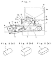
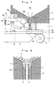
- Figs. 1 to 16 illustrate a preferred embodiment of the present invention, in which reference numeral 1 denotes a frame, 2 denotes a hopper, 3 denotes a fixed pipe, 4 denotes a movable pipe, 5 denotes a component guide, 6 denotes a belt guide, 7 denotes a belt, 8 denotes a pair of front and rear pulleys, 9 denotes a stopper, 10 denotes a pipe raising/lowering mechanism, 11 denotes a belt delivery mechanism, and 12 denotes a stopper displacement mechanism.
- reference numeral 1 denotes a frame
- 2 denotes a hopper
- 3 denotes a fixed pipe
- 4 denotes a movable pipe
- 5 denotes a component guide
- 6 denotes a belt guide
- 7 denotes a belt
- 8 denotes a pair of front and rear pulleys
- 9 denotes a stopper
- 10 denotes a pipe raising
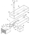
- the hopper 2 comprises as shown in Figs. 1 and 7 an accommodation chamber 2a, a cover plate 2b for covering the upper end opening of the accommodation chamber 2a in which the cover plate 2b freely opens and shuts, and a circular sliding hole 2c for the movable pipe which extends through the bottom surface of the accommodation chamber 2a, with the side surface of the hopper 2 being removably mounted on the frame 1.
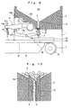
- a multiplicity of chip components P having a cylindrical, a prism-like or a flat prism-like shape shown in Figs. 2(a), 2(b) or 2(c), respectively, for example, a type of chip components represented by chip capacitors, chip inductors, chip resistors, etc.
- the chip component P has an external electrode and an internal conductor or the like; at least one of the electrode or internal conductor includes at least a portion having high magnetic permeability so the chip component is capable of being attracted by a permanent magnet.
- the chip components P accommodated in the hopper 2 are moved by their own weight toward the circular sliding hole 2c along an inclined bottom surface with the supply of the components.
- the fixed pipe 3 is made of a circular pipe member having a predetermined length and is fixed at its lower end to the component guide 5 and passes centrally vertically through the circular sliding hole 2c with the positional relationship in which its upper end is slightly lower than the upper end of the circular sliding hole 2c.
- the fixed pipe 3 has a thickness less than the maximum length of the end surface of the chip components P to be fed.
- the diameter of the bore of the fixed pipe 3 (vertical passage) is slightly larger than the maximum length of the end surface of the chip components P to be fed, allowing the chip components P within the accommodation chamber 2a to be taken one by one into the upper end opening of the fixed pipe 3 with the longitudinal orientation to be moved by their own weight through the interior of the fixed pipe 3 with the same orientation.
- the movable pipe 4 is made of a circular pipe member having a predetermined length and having an outer diameter slightly smaller than the diameter of the circular sliding hole 2c and an inner diameter slightly larger than the outer diameter of the fixed pipe 3, with a positional relationship in which its upper end is lower than the upper end of the fixed pipe 3, the movable pipe 4 being arranged in a vertically movable manner outside the fixed pipe 3.
- the movable pipe 4 has a thickness slightly larger than the maximum length of the end surface of the chip components P to be fed and has on its upper end surface a guide surface 4a of a conical shape extending in a downward inclined manner toward its center.
- the intermediate portion and the lower end portion of the external surface of the movable pipe 4 are formed with engagement collars 4b and 4c, respectively, the intermediate engagement collar 4b having coiled springs S1 and S2 arranged on its top and bottom with a relationship of biasing force expressed by S1 ⁇ S2.
- the component guide 5 consists of four blocks B1 to B4.
- the block B1 has in its bottom surface a linear groove B1a having the predetermined width W3 and depth D3 corresponding to the chip components P to be fed.
- the front part of the block B1 is provided with a component take-out port B1b (see Fig. 15) for allowing the top surface of the foremost chip component P to be exposed to the exterior.
- the rear part of the block B1 is provided with a protrusion B1c for registering with the block B3.
- the block B2 has a through insertion hole B2a for the fixed pipe 3.
- the bottom surface of the block B2 is provided with two protrusions B2b for registering with the block B3.
- the front part of the block B3 is notched on one side, the notched portion having in its inner side surface a groove B3a of a combination in shape of a curved groove and a linear groove.
- the top surface of the block B3 is provided with two holes B3b corresponding to the protrusion B2b of the block B2.
- the front part of the block B3 is provided with holes B3c and B3d corresponding respectively to the protrusion B1c of the block B1 and to a protrusion B4a of the block B4.
- the block B4 is of the same shape as the notched portion of the block B3.
- the side surface of the block B4 is provided with the protrusion B4a for registering with the block B3.
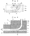
- the groove B3a of the block B3 is of a combination in shape of a curved groove T1 having at its center a predetermined radius of curvature rs and a linear groove T2 continuous with the curved groove T1.
- the linear groove T2 has the width W2 equal to that of the curved groove T1 but its depth D2 is smaller than the depth D1 of the curved groove T1.
- the groove B3a of the block B3 is so contoured that a plane parallel to the linear groove T2 removes the portions beyond the range of angle ⁇ 2 of the curved groove T1 and the lower portion (which is indicated by a dotted line in Fig. 4) of the linear groove T2.
- the width W3 of the linear groove B1a of the block B1 is coincident with the width W1 of the curved groove T1 and with the width W2 of the linear groove T2 and that its depth D3 coincides with the depth D1 of the curved groove T1.
- the four blocks B1 to B4 are assembled into the component guide 5, which is fixedly mounted by its side surface to the frame 1.
- Fig. 5 which is a longitudinal sectional view of its major part, the bottom surface of the block B1 is in contact with the surface of the belt 7 whereas the bottom surfaces of the blocks B3 and B4 do not contact with the surface of the belt 7, forming a gap therebetween corresponding to the difference between the depths D3 and D2.
- the curved groove T1 of the groove B3a of the block B3 is closed at its side opening by the block B4, resulting in a curved passage Tx having a predetermined radius of curvature rs at its passage center and having an opening Tt for the discharge of the chip components in the vicinity of the belt.
- the linear groove T2 of the groove B3a is closed at its side opening by the block B4 and at its bottom opening by the belt 7, resulting in a linear passage Ty, besides the linear groove B1a of the block B1 is closed at its bottom opening by the belt 7, resulting in a linear passage Tz.
- the linear passages Ty and Tz are continuous with each other in such a manner that their top surfaces are level with each other, and are become a transverse passage for transporting said chip components in a predetermined direction.
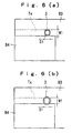
- Figs. 6(a) and 6(b) are top plan views showing the state of connection of the fixed pipe 3 with the curved passage Tx.
- Fig. 6(a) illustrates a case where the diameter of the bore of the fixed pipe 3 is not more than the inlet depth D1 of the curved passage Tx.
- Fig. 6(b) illustrates a case where the diameter of the bore of the fixed pipe 3 is equal to or more than the inlet depth D1 and not more than the inlet width W1 of the curved passage Tx.
- the belt guide 6 has in its top surface a linear groove 6a of predetermined width and depth corresponding to the belt 7, and being arranged below the component guide 5 in such a manner that the center in the width direction of the linear groove 6a coincides with the centers in the width direction of the linear passages Ty and Tz, besides being fixedly mounted at its side to the frame 1.
- the belt 7 is comprised of a non-magnetic flat belt or a timing belt made of a synthetic rubber or a soft resin.
- the belt 7 is wound on the pair of pulleys 8 rotatably supported by the frame 1 at the positions anterior and posterior to the belt guide 6, with its upper part being positioned within the linear groove 6a of the belt guide 6 in such a manner that the upper part is brought into movable contact with the bottom surface of the component guide 5 by the winding tension.
- the stopper 9 is comprised of a non-magnetic rectangular plate having a thickness closer to the depth of the linear passage Tz.
- the stopper 9 is supported at its one end via a pin 9a by a stopper support member 9b in a horizontally movable manner.
- the stopper 9 is urged by a coiled spring S3 in the counterclockwise direction in Fig. 15, to secure a predetermined component stop position when one surface of the stopper 9 abuts against the front end or its vicinity of the linear passage Tz (See Fig. 16).
- the stopper 9 has an attracting section MS comprised of a rectangular parallelepiped rare-earth permanent magnet, which is so oriented that either its north pole or south pole surfaces is allowed to abut against the foremost chip component P.
- a single permanent magnet comprising the attracting section MS is one having a height substantially equal to the height of the chip component P to be fed and having a width larger than the width of the chip component P to be fed, the permanent magnet may have a height smaller than the height of the chip component P as well as a width less than the width of the chip component P.
- the stopper support member 9b for rotatably supporting the stopper 9 is attached at its one end via a pin 9c to the front part of the component guide 5 in an upwardly rotatable manner. More specifically, the stopper 9 is so adapted to be kept horizontally by engaging the front part of the stopper support member 9b with a plate spring 9d disposed on the front end of the component guide 5, and to come apart upward from the belt 7 by releasing the engagement with the plate spring 9d to upward turn the stopper support member 9b. In other words, an upward separation of the stopper 9 from the belt 7 by the upward movement of the stopper support member 9b will allow the chip components P residing within the linear passage Tz to be discharged from the front end of the linear passage Tz to the exterior.
- the pipe raising/lowering mechanism 10 comprises as shown in Fig. 7 an operating lever 10a, a relay lever 10b arranged below the operating lever 10a, and a positioning stopper 10c for defining a position to which the operating lever 10a returns.
- the operating lever 10a is supported at its one end by a pin 10d provided on the frame 1, to allow a rotation in the vertical direction. In its standby mode the intermediate top surface of the operating lever 10a is abutted against the positioning stopper 10c.
- the relay lever 10b is supported at its central part by a pin 10e disposed on the frame 1, to allow a rotation in the vertical direction.
- the relay lever 10b has a circular hole portion or a U-shaped portion formed at one end (right end portion in the drawing) and adapted to be disposed between the lower collar 4c of the movable pipe 4 and the lower coiled spring S2. In its standby mode the relay lever 10b is downward biased by the upper coiled spring S1 and the lower coiled spring S2, to bring a roller 10f provided on the other end into abutment against the center bottom surface of the operating lever 10a.
- the positioning stopper 10c is comprised of a disk and a screw for fixing the disk at an eccentric position so as to allow an optional adjustment of the returning position of the operating lever 10a, that is, a lowering position of the movable pipe 4, by varying the orientation of the fixing of the disk. For instance, by displacing the positioning stopper 10c to the position indicated by a dotted line in Fig. 7, the returning position of the operating lever 10a is shifted downward from the position indicated by a solid line, to allow an upward displacement of the lowering position of the movable pipe 4.
- the downward pressing force F is applied to the end of the operating lever 10a, to rotate the operating lever 10a around the pin 10d in the counterclockwise direction, to cause the bottom surface of the operating lever 10a to apply the downward force to the roller 10f of the relay lever 10b to rotate the relay lever 10b around the pin 10e in the counterclockwise direction, thereby allowing the upward movement of the movable pipe 4 while compressing the coiled spring S1 via the coiled spring S2 by the end portion of the relay lever 10b.
- the belt delivery mechanism 11 comprises as shown in Figs. 11 and 12 an operating lever 11a, a relay lever 11b rotatably coupled to the operating lever 11a, a delivery lever 11c rotatably coupled to the relay lever 11b and coaxially rotationally with the front side pulley 8, a pawl 11d rotatably provided on the delivery lever 11c, a ratchet wheel 11e coaxially fastened to the front side pulley 8, a positoining stopper 11f for defining a return position of the operating lever 11a, a positioning stopper 11g for defining a rotation limit position of the operating lever 11a, a coiled spring S4 for biasing the operating lever 11a in the clockwise direction in the drawing, and a coiled spring S5 for bringing the pawl 11d into pressure contact with the ratchet wheel 11e.
- the operating lever 11a is supported at its one end by the pin 10d common to the pipe raising/lowering mechanism 10 to allow a vertical rotation. In its standby state, the operating lever 11a is abutted at its lever side surface center against the positioning stopper 11f by biasing force of the coiled spring S4.
- the operative site of the operating lever 11a of the belt delivery mechanism 11 vertically confronts the operative site of the operating lever 10a of the above-described pipe raising/lowering mechanism 10, thereby enabling the downward pressing force F applied to the end of the operating lever 10a of the pipe raising/lowering mechanism 10 to be transmitted via the coiled spring SS to the end of the operating lever 11a of the belt delivery mechanism 11.
- the positioning stopper 11g comprises a disk and a screw for fixing the disk at an eccentric position.
- the disk fixing orientation is varied to arbitrarily adjust the rotation limit position of the operating lever 11a, that is, a delivery amount of the belt 7. For example, a shift of the positioning stopper 11g to the position indicated by a dotted line in Fig. 12 will result in a rightward shift of the rotation limit position of the operating lever 11a from the position indicated by a solid line, thereby increasing the amount of delivery of the belt.
- the downward pressing force F is applied to the end of the operating lever 10a of the pipe raising/lowering mechanism 10 to transmit this force via the coiled spring SS to the end of the operating lever 11a, thereby as shown in Fig. 12 enabling the operating lever 11a to rotate around the pin 10d against biasing force of the coiled spring S4 in the counterclockwise direction and enabling the delivery lever 11c to rotate via the relay lever 11b in the counterclockwise direction, to consequently cause the ratchet wheel 11e engaging with the pawl 11d of the delivery lever 11c to rotate together with the front side pulley 8 in the counterclockwise direction, allowing forward movement of the belt 7 by a distance corresponding to the rotational angle.
- the stopper displacement mechanism 12 comprises as shown in Figs. 11 and 15 a ratchet wheel 12a coaxially mounted to the front side pulley 8, a stopper actuating plate 12c rotatably attached via a pin 12b to the side surface of the frame 1, a coiled spring S6 for forward biasing the stopper actuating plate 12c to bring its protrusion 12c' into pressure contact with the ratchet wheel 12a, a component retainer lever 12e horizontally movably attached to front part of the component guide 5 by a pin 12d, a coiled spring S7 for biasing the component retainer lever 12e in the clockwise direction in the drawing, a component retainer pin 12f which is inserted into a hole B1d formed in the front part side surface of the linear passage Tz, and a coiled spring S8 for outwardly biasing the component retainer pin 12f.
- the pressing of the stopper actuating plate 12c displaces the stopper 9 forward (the component take-out position apart forward from the component stop position) to allow the foremost chip component P to be forward displaced together with the stopper 9 to which the foremost chip component P adheres by the attracting force of the attracting section MS, thus separating them from the succeeding chip components P.
- the stopper displacement mechanism 12 allow the stopper actuating plate 12c to be moved backward by a predetermined distance by making use of the undulation of one ratchet of the ratchet wheel 12a.
- the stopper 9 is abutted by biasing force of the coiled spring S3 against the front end of the linear passage Tz to secure the component stop position.
- a rear end protrusion 12e' of the component retainer lever 12e is forced by the stopper actuating place 12c inward against biasing force of the coiled spring S7 to rotate in the counterclockwise direction in the drawing, so that the component retainer pin 12f moves outward by biasing force of the coiled spring S8, to release the retaining of the second foremost chip component P, thus allowing an aligned transport of the chip components P within the linear passage Tz.
- annular pocket E among the upper end of the movable pipe 4 and the inner surface of the circular sliding hole 2c and the outer surface of the fixed pipe 3, the annular pocket E receiving few components P.
- the component P within the annular pocket E is upward moved by the movable pipe 4 to release the accommodated components within the accommodation chamber 2a, and the chip components P resting on the fixed pipe 3, if any, could be thrust aside therefrom.
- the accommodated components P within the hopper 2 is taken one by one into the upper end opening of the fixed pipe 3 in the longitudinal direction by utilizing the inclination of the upper end guide surface 4a of the movable pipe 4.
- the chip components P taken into the fixed pipe 3 are moved by their own weights within the fixed pipe 3 with the same orientation.
- the take-in operation of the components into fixed pipe 3 is performed both in the raising process and the lowering process of the movable pipe 4 in this manner, and the chip components P taken one by one into the fixed pipe 3 with the longitudinal orientation as shown in Figs. 10 and 13 are moved by their own weights through the bore of the fixed pipe 3 and enter the downstream curved passage Tx with the same orientation.
- the chip components P enter the curved passage Tx with the orientation (that is, the orientation in the rotational direction around the vertical axis) matching the contour of the inlet of the curved passage Tx.
- the posture of the chip components P which have entered the curved passage Tx is varied from the vertical orientation to the transverse orientation (about 75 degrees in the drawings).
- the chip components P are discharged onto the belt 7 with the same orientation from the opening Tt disposed on the extremity at the lower part of the curved passage Tx, to abut their tips against the surface of the belt 7.
- the stopper actuating plate 12c is retreated by a predetermined distance by the ratchet wheel 12a of the stopper displacement mechanism 12 rotating in the same direction, whereupon the spring biasing force causes a backward displacement of the stopper 9, allowing the stopper 9 to abut against the front end of the linear passage Tz to secure the desired component stop position. More specifically, the chip components P transported in alignment during the belt movement are stopped by the abutment against the stopper 9 and are aligned without gaps therebetween with the longitudinal orientation in the state where the foremost chip components P abuts against the stopper 9.
- the intermittent movement of the belt 7 is so preset as to be slightly larger than the longitudinal dimension of the chip components P, only the belt 7 is allowed to slightly advance with the aid of the sliding action relative to the component contact surface even after the stopper 9 has brought the chip component P transported in alignment to a rest (see Fig. 16).
- the stopper actuating plate 12c is rotationally returned so that as shown in Fig. 15 the rotational return of the component retainer lever 12e will allow the tip of the component retainer pin 12f to project into the linear passage Tz to retain the second foremost chip components P.
- the stopper 9 is forward displaced and separated from the front end of the linear passage Tz, and the foremost chip component adhered to the stopper 9 by the magnetic force of the attracting section Ms is moved to the component take-out position together with the stopper 9 to come apart from the succeeding chip components P, to compulsorily form a gap C between the foremost chip component P and the succeeding chip components P.
- the take-out action of the foremost chip component P by the attracting nozzle or the like is carried out as shown in Fig. 15 in the state where the foremost chip component P is displaced to the component take-out position together with the stopper 9 and is separated from the succeeding chip components P. For this reason, adhesion and entanglement between the foremost chip component P and the succeeding chip components P due to the influence of humidity or the like would be easily canceled to ensure a take-out with a stabilized posture without any interference between the foremost chip component P and the succeeding chip components P.
- the curved passage Tx having at its passage center a predetermined radius of curvature rs is provided between the bore (vertical passage) of the fixed pipe 3 and the linear passages Ty and Tz (transverse passage) for use in the transport of components, thereby ensuring the smooth movement of the components through the curved passage Tx with its improved posture change, even in the case of handling chip components of small in size and extremely light-weight per each.
- the provision of the opening Tt for the discharge of the chip components in the vicinity of the transverse passage of the curved passage Tx would achieve a smooth discharge action of the chip components P from the curved passage Tx to the transverse passage, thus ensuring an improved desired component discharge even in the case of handling chip components having greater lengths.
- the opening Tt for the discharge of the chip components is formed by setting to be smaller than 90 degrees the angular range ⁇ 2 relative to its upper end, of the curved surface (second curved surface T1b) constituting the curved passage Tx, so that the discharge action of the chip components P onto the transverse passage can be maintained properly by adjusting the angular range ⁇ 2 in response to the sizes of the chip components to be fed.
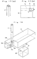
- a pipe of a square section as shown in Fig. 17(a) may be used as a fixed pipe 3' in the case of feeding the prism-shaped or flat prism shaped chip components as shown in Fig. 2(b) or 2(c), respectively.
- the fixed pipe 3' use may be made of a square pipe member having inner dimensions corresponding to the inlet width W1 and depth D1 of the curved passage Tx or having inner dimensions smaller than those, as shown in Fig. 17(b).
- the movable pipe 4 may be comprised of a square pipe member or a circular pipe member having a square bore and a circular exterior.
- Fig. 18 illustrates an embodiment in which the construction of the component guide is improved. This embodiment differs in construction from the embodiment shown in Figs. 1 to 16 in that the component guide consists of three blocks. It is to be noted that the block corresponding to the block B1 has the same construction and hence is omitted from the drawing. The other constructions are substantially the same as the embodiment shown in Figs. 1 to 16 and are also omitted in this description.
- a block G1 illustrated in Fig. 18 is notched in its front part at one side, the inner side surface of the notched portion being provided with a groove G1a equivalent to the groove B3a and with a recess G1b comprising an insertion hole for the fixed pipe 3.
- the front part of the block G1 is provided with holes G1c and G1d for registering with the other blocks.
- a block G2 has the same contour as the notched portion of the block G1.
- the side surface of the block G2 is formed with a recess G2a for constituting the pipe insertion hole in cooperation with the recess G1b of the block G1, and with a protrusion G2b for registering with the hole G1c of the block G1.
- the block G2 is fitted into the notched portion of the block G1 to form a curved passage similar to the embodiment of Figs. 1 to 16.
- the recesses G1b and G2a of the blocks G1 and G2 cooperate to form the insertion hole for the fixed pipe 3.
- the fixed pipe 3 inserted into the insertion hole is abutted at its lower end against the step on the top surface of the curved passage and is connected to the curved passage.
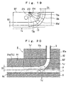
- Fig. 19 illustrates an another embodiment in which the construction of the component guide is improved. This embodiment differs in construction from the embodiment shown in Figs. 1 to 16 in that the groove of the block B3 has an improved configuration.
- the other constructions are substantially the same as the embodiment shown in Figs. 1 to 16 and hence are not described herein.
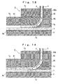
- a block B3' shown in Fig. 19 has a front part notched on its one sides, the inner side surface of the notched portion being provided with a groove B3a' comprised of a combination of a curved groove T3 having at its center a predetermined radius of curvature rs and a linear groove T4 continuous with the curved groove T3.
- the curved groove T3 includes a first curved surface T3a having a radius of curvature r1 smaller than the central curvature rs and having an angular range ⁇ 3 of about 45 degrees from its upper end, a second curved surface T3b having a radius of curvature r2 larger than the central curvature rs and having an angular range ⁇ 4 of about 52.5 degrees from the upper end, and an inclined surface T3c having an angle of inclination of about 75 degrees relative to the perpendicular and having an angular range ⁇ 5 of about 27.5 degrees from the lower end of the first curved surface T3a.
- the angular range ⁇ 5 is set so that an angle of the inclined surface T3c has an acute angle to the vertical passage or the transverse passage.
- the curved groove T3 presents a certain section (a rectangular shape defined by the width W1 and the depth D1).
- the linear groove T4 has the same width W2 as that of the curved groove T3, but its depth D2 is smaller than the depth D1 of the curved groove T3.
- the groove B3a'of the block B3' has a configuration obtained by removing by a plane parallel to the linear groove T4 both the portion beyond the angular range ⁇ 4 of the curved groove T3 and the lower part of the linear groove T4 (dotted portion in Fig. 19).
- the curved groove T3 and the top surface of the linear groove T4 are continuous with each other by way of the inclined surface T3c.
- the block B3' shown in Fig. 19 is assembled with the other three blocks B1, B2 and B4 shown in Figs. 1 to 16 into the component guide 5, of which side surface is fixedly secured to the frame 1.
- Fig. 20 illustrating the longitudinal section of its principal part, the bottom surface of the block B1 abuts against the surface of the belt 7 but the bottom surfaces of the blocks B3' and B4 are not abutted against the surface of the belt 7, to form a gap therebetween corresponding to the difference between the depths D3 and D2.
- the curved groove T3 of the groove B3a' of the block B3' is closed at its side opening by the block B4, resulting in a curved passage Tx' having at its center a predetermined radius of curvature rs and having in the vicinity of the belt an opening Tt' for the discharge of the chip components.
- the linear groove T4 of the groove B3a' is closed at its side opening by the block B4 and is closed at its bottom opening by the belt 7, resulting in a linear passage Ty'
- the linear groove B1a of the block B1 is closed at its bottom opening by the belt 7, resulting in a linear passage Tz.
- the linear passages Ty' and Tz are continuous with each other in such a manner that their top surfaces are coincident with each other.
- the inclined surface T3c located thereabove will suppress jumping which would otherwise occur when the chip components P traveling through the curved passage Tx' are discharged via the opening Tt' onto the belt 7 (see the dotted lines in Fig. 20), thereby preventing the posture of the chip components P discharged onto the belt 7 from being disturbed.
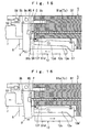
- Figs. 21 and 22 illustrate two different embodiments each having permanent magnets arranged along the curved passage. These embodiments differ in construction from the embodiment shown in Figs. 1 to 16 in that permanent magnets are arranged along the curved passage Tx for drawing the chip components P by the magnetic force toward the inner surface of the passage without interfering with the movement of the chip components P.
- the other constructions are substantially the same as those of the embodiment shown in Figs. 1 to 16 and therefore are not described herein.
- Fig. 21 embodiment is provided with a plurality of small sized permanent magnets MC1 (rare earth permanent magnets) equally spaced apart from one another along the curved passage Tx.
- the permanent magnets MC1 may be exposed to the curved passage Tx or may not be exposed to it.
- the polarities of the permanent magnets MC1 closer to the curved passage Tx are such that N-pole and S-pole alternate along the curved passage Tx.
- Fig. 22 embodiment is provided with a plurality of small sized permanent magnets MC2 (rare earth permanent magnets) equidistantly arranged along the curved passage Tx.
- the permanent magnets MC2 may or may not be exposed to the curved passage Tx.
- the polarities of the permanent magnets MC2 closer to the curved passage Tx are such that N-pole and S-pole alternate along the curved passage Tx.
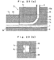
- Figs. 23(a) and 23(b) illustrate another embodiment of the present invention, which differs from the embodiment shown in Figs. 1 to 16 in that the inner surface of the curved passage Tx is provided with a convexity PL for restricting the posture of the chip components P passing though the curved passage Tx.
- the convexity PL has a cross section shape of a semi-circular or other similar curved surface shape, and is formed along the curved passage Tx at the center of the front curved surface constituting the curved passage Tx.
- the other structures are substantially the same as those of the embodiment shown in Figs. 1 to 16, and hence the description thereof will be omitted.
- the convexity PL will contribute to a restriction of the posture and the path of movement of the chip components P moving through the curved passage Tx, to ensure the smooth movement of the components through the curved passage Tx.
- the grooves B3a (B3a') and G1a of the blocks B3 (B3') and G1, respectively, are shown including the linear grooves
- the blocks B3 (B3') and G1 may be replaced by any blocks having only the curved grooves which are obtained by excluding the linear grooves from the grooves B3a (B3a') and G1a.
- the curved passages Tx and Tx' will be able to obtain higher wear resistant properties compared with the blocks made of resin or metal, while simultaneously preventing any variance in passage dimensions from occurring even under high temperature and high humidity environment, to provide an improved stability to the change of posture and to the discharge of components.
- the above embodiments employ a belt to close the underside of the linear groove to form a linear transverse passage for the transport of chip components
- the underside of the linear groove may be closed by any fixed part other than the belt to make the similar transverse passage.
- air may be blown in from the rear side of the transverse passage or alternatively, air may be sucked in from the front side of the transverse passage.
Landscapes
- Engineering & Computer Science (AREA)
- Manufacturing & Machinery (AREA)
- Microelectronics & Electronic Packaging (AREA)
- Supply And Installment Of Electrical Components (AREA)
- Feeding Of Articles To Conveyors (AREA)
Claims (9)
- Zuführungsvorrichtung für Chip-Komponenten, mit einer Vorratskammer (2a) zur Bevorratung von Chip-Komponenten (P) im aufgeschütteten Zustand, einem senkrechten Kanal (3), in welchen die Chip-Komponenten (P) aufeinanderfolgend aufgenommen werden und in welchem sie sich aufgrund ihres Eigengewichtes bewegen können, und einem Querkanal (Ty,Tz,Ty'), durch welchen die aus dem senkrechten Kanal (3) ausgegebenen Chip-Komponenten (P) in einer vorbestimmten Richtung befördert werden, sowie mit:dadurch gekennzeichnet, daß der gekrümmte Kanal eine Öffnung (Tt,Tt') zur Ausgabe von Chip-Komponenten (P) in der Nähe des Querkanals (Ty,Tz,Ty') aufweist.einem gekrümmten Kanal (Tx,Tx'), der zwischen dem senkrechten Kanal (3) und dem Querkanal (Ty,Tz,Ty') angeordnet ist, zum Verändern der Lage der aus dem senkrechten Kanal (3) in den Querkanal Ty,Tz,Ty') ausgegebenen Chip-Komponenten (P), so daß diese dem Querkanal (Ty,Tz,Ty') entspricht,welcher gekrümmte Kanal (Tx,Tx') in seiner Kanal-Mitte einen vorbestimmten Krümmungsradius aufweist,
- Zuführungsvorrichtung für Chip-Komponenten gemäß Anspruch 1, bei welcher der gekrümmte Kanal (Tx,Tx') eine erste gekrümmte Oberfläche (T1a,T3a) mit einem vorbestimmten Krümmungsradius aufweist, sowie eine zweite gekrümmte Oberfläche (T1b,T3b), deren Krümmungsmittelpunkt mit demjenigen der ersten gekrümmten Oberfläche (T1a,T3a) zusammenfällt und deren Krümmungsradius größer ist als derjenige der ersten gekrümmten Oberfläche (T1a,T3a), und
ein Winkelbereich der zweiten gekrümmten Oberfläche (T1b,T3b) von ihrem oberen Ende her kleiner bemessen ist als 90 Grad, so daß die Öffnung (Tt,Tt') zur Ausgabe der Chip-Komponenten (P) in der Nähe des Querkanals (Ty,Tz,Ty') gebildet wird. - Zuführungsvorrichtung für Chip-Komponenten gemäß Anspruch 2, bei welcher ein Winkelbereich der ersten gekrümmten Oberfläche (T1a) von deren oberem Ende her größer ist als der Winkelbereich der zweiten gekrümmten Oberfläche (T1b) von deren oberem Ende her.
- Zuführungsvorrichtung für Chip-Komponenten gemäß Anspruch 2, bei welcher ein Winkelbereich der ersten gekrümmten Oberfläche (T3a) von deren oberem Ende her kleiner ist als der Winkelbereich der zweiten gekrümmten Oberfläche (T3b) von deren oberem Ende her, und
die erste gekrümmte Oberfläche (T3a) an ihrem unteren Ende mit einer geneigten Oberfläche (T3c) versehen ist, welche sich in einem spitzen Winkel an den senkrechten Kanal (3) anschließt. - Zuführungsvorrichtung für Chip-Komponenten gemäß einem der Ansprüche 1 bis 4, bei welcher der gekrümmte Kanal (Tx,Tx') einen Block (B3,G1,B3') mit einer gekrümmten Nut (B3a,G1a,B3a') sowie einen Block (B4,G2) zum Verschliessen der gekrümmten Nut (B3a,G1a,B3a') umfaßt, und zumindest der Block mit der gekrümmten Nut (B3a,G1a,B3a') aus Keramik besteht.
- Zuführungsvorrichtung für Chip-Komponenten gemäß einem der Ansprüche 1 bis 5, mit einem Dauermagneten (MC1,MC2), der entlang des gekrümmten Kanals (Tx,Tx') zum Anziehen der sich durch den gekrümmten Kanal (Tx,Tx') bewegenden Chip-Komponenten (P) durch seine Magnetkraft an die innere Oberfläche des gekrümmten Kanals (Tx,Tx') angeordnet ist, ohne daß die Bewegung der Chip-Komponenten (P) gestört wird.
- Zuführungsvorrichtung für Chip-Komponenten gemäß Anspruch 6, bei welcher der Dauermagnet (MC1,MC2) kleine Magnete umfaßt.
- Zuführungsvorrichtung für Chip-Komponenten gemäß einem der Ansprüche 1 bis 7, bei welcher die innere Oberfläche des gekrümmten Kanals (Tx,Tx') mit einer konvexen Wölbung (PL) versehen ist, zur Festlegung der Lage der den gekrümmten Kanal (Tx,Tx') passierenden Chip-Komponenten (P).
- Zuführungsvorrichtung für Chip-Komponenten gemäß Anspruch 8, bei welcher der Querschnitt der konvexen Wölbung (PL) die Form eines Halbkreises oder eine dementsprechend gekrümmte Oberflächenform aufweist.
Applications Claiming Priority (3)
| Application Number | Priority Date | Filing Date | Title |
|---|---|---|---|
| JP29042096 | 1996-10-31 | ||
| JP29042096 | 1996-10-31 | ||
| JP290420/96 | 1996-10-31 |
Publications (3)
| Publication Number | Publication Date |
|---|---|
| EP0840544A2 EP0840544A2 (de) | 1998-05-06 |
| EP0840544A3 EP0840544A3 (de) | 1999-12-08 |
| EP0840544B1 true EP0840544B1 (de) | 2003-01-15 |
Family
ID=17755807
Family Applications (1)
| Application Number | Title | Priority Date | Filing Date |
|---|---|---|---|
| EP97118350A Expired - Lifetime EP0840544B1 (de) | 1996-10-31 | 1997-10-22 | Speisevorrichtung für elektronische Komponenten |
Country Status (6)
| Country | Link |
|---|---|
| US (1) | US6032783A (de) |
| EP (1) | EP0840544B1 (de) |
| KR (1) | KR100277370B1 (de) |
| CN (1) | CN1112090C (de) |
| DE (1) | DE69718416T2 (de) |
| TW (1) | TW394496U (de) |
Families Citing this family (25)
| Publication number | Priority date | Publication date | Assignee | Title |
|---|---|---|---|---|
| JPH1149337A (ja) * | 1997-07-30 | 1999-02-23 | Potsupuman:Kk | チップ部品供給装置 |
| JPH11177285A (ja) * | 1997-12-09 | 1999-07-02 | Taiyo Yuden Co Ltd | チップ部品供給装置 |
| JP4141004B2 (ja) | 1998-03-04 | 2008-08-27 | 太陽誘電株式会社 | チップ部品供給装置 |
| JP3259680B2 (ja) * | 1998-04-07 | 2002-02-25 | 株式会社村田製作所 | チップ状電子部品供給装置 |
| JP3430919B2 (ja) | 1998-05-15 | 2003-07-28 | 株式会社村田製作所 | 部品搬送装置 |
| JP3244047B2 (ja) * | 1998-05-15 | 2002-01-07 | 株式会社村田製作所 | 部品搬送装置 |
| US6116840A (en) * | 1998-08-21 | 2000-09-12 | Taiyo Yuden Co., Ltd. | Component supply apparatus |
| JP3582381B2 (ja) * | 1998-11-09 | 2004-10-27 | 株式会社村田製作所 | 部品搬送装置 |
| JP3794902B2 (ja) * | 2000-06-05 | 2006-07-12 | 太陽誘電株式会社 | 電子部品供給装置 |
| JP4587556B2 (ja) * | 2000-07-03 | 2010-11-24 | 太陽誘電株式会社 | 電子部品供給装置 |
| KR20060124723A (ko) * | 2004-01-26 | 2006-12-05 | 가부시키가이샤 포프만 | 전자부품 자동장착장치 및 부품재고 관리장치 |
| KR101107593B1 (ko) * | 2004-09-07 | 2012-01-25 | 엘지이노텍 주식회사 | 칩 공급장치 |
| ATE343520T1 (de) * | 2005-03-02 | 2006-11-15 | Uhlmann Pac Systeme Gmbh & Co | Zuführrohr für tabletten |
| DE102005018651A1 (de) * | 2005-04-21 | 2006-10-26 | Uhlmann Pac-Systeme Gmbh & Co Kg | Vorrichtung zum Orientieren und Weitertransport von Schüttgut |
| DE102005058704B3 (de) * | 2005-12-08 | 2007-07-12 | Multitest Elektronische Systeme Gmbh | Führungsbahn für elektronische Bauelemente |
| US7464803B2 (en) * | 2006-07-24 | 2008-12-16 | Eastman Kodak Company | Orientating apparatus |
| CN104097932B (zh) * | 2013-04-07 | 2016-03-09 | 上海吉田拉链有限公司 | 小工件的输送方法和输送装置 |
| GB201405342D0 (en) | 2014-03-25 | 2014-05-07 | British American Tobacco Co | Feed unit |
| GB201405340D0 (en) * | 2014-03-25 | 2014-05-07 | British American Tobacco Co | Feed Unit |
| GB201405341D0 (en) | 2014-03-25 | 2014-05-07 | British American Tobacco Co | Feed unit |
| GB201405337D0 (en) | 2014-03-25 | 2014-05-07 | British American Tobacco Co | Feed unit |
| KR101981512B1 (ko) * | 2014-03-27 | 2019-05-23 | 가부시키가이샤 무라타 세이사쿠쇼 | 자세 변환 장치·정렬 장치 및 자세 변환 방법·정렬 방법 |
| WO2017090112A1 (ja) * | 2015-11-25 | 2017-06-01 | 富士機械製造株式会社 | テープ湾曲アタッチメント及びフィーダ |
| US9975708B2 (en) * | 2016-03-16 | 2018-05-22 | Texas Instruments Incorporated | Transfer track stopper for packaged integrated circuits |
| WO2022009646A1 (ja) | 2020-07-07 | 2022-01-13 | 株式会社村田製作所 | 収納ケース |
Family Cites Families (8)
| Publication number | Priority date | Publication date | Assignee | Title |
|---|---|---|---|---|
| JPH0730572Y2 (ja) * | 1990-05-31 | 1995-07-12 | 太陽誘電株式会社 | 電子部品供給装置 |
| JP3453809B2 (ja) * | 1992-12-10 | 2003-10-06 | 松下電器産業株式会社 | チップ部品供給装置およびチップ部品供給方法 |
| TW348933U (en) * | 1992-12-10 | 1998-12-21 | Matsushita Electric Industrial Co Ltd | Chip component supply equipment |
| SE9300643L (sv) * | 1993-02-26 | 1994-08-27 | Ips Mechatronics Ab | Förfarande och anordning för att mata fram föremål till visst korrekt hanteringsläge |
| JPH07212084A (ja) * | 1994-01-24 | 1995-08-11 | Matsushita Electric Ind Co Ltd | 部品供給装置 |
| EP1771058A3 (de) * | 1994-05-18 | 2007-06-13 | Taiyo Yuden Co., Ltd. | Einrichtung und Verfahren für die Lieferung von Chipkomponenten |
| JP3642071B2 (ja) * | 1994-08-09 | 2005-04-27 | 松下電器産業株式会社 | チップ部品供給装置 |
| JPH08107294A (ja) * | 1994-10-03 | 1996-04-23 | Sony Corp | 部品供給方法及びその装置 |
-
1997
- 1997-10-21 TW TW086217788U patent/TW394496U/zh not_active IP Right Cessation
- 1997-10-22 EP EP97118350A patent/EP0840544B1/de not_active Expired - Lifetime
- 1997-10-22 DE DE69718416T patent/DE69718416T2/de not_active Expired - Lifetime
- 1997-10-22 KR KR1019970054129A patent/KR100277370B1/ko not_active Expired - Fee Related
- 1997-10-22 US US08/955,566 patent/US6032783A/en not_active Expired - Fee Related
- 1997-10-22 CN CN97121324A patent/CN1112090C/zh not_active Expired - Fee Related
Also Published As
| Publication number | Publication date |
|---|---|
| CN1181689A (zh) | 1998-05-13 |
| CN1112090C (zh) | 2003-06-18 |
| DE69718416D1 (de) | 2003-02-20 |
| EP0840544A2 (de) | 1998-05-06 |
| US6032783A (en) | 2000-03-07 |
| TW394496U (en) | 2000-06-11 |
| DE69718416T2 (de) | 2003-09-25 |
| KR100277370B1 (ko) | 2001-01-15 |
| EP0840544A3 (de) | 1999-12-08 |
| KR19980033044A (ko) | 1998-07-25 |
Similar Documents
| Publication | Publication Date | Title |
|---|---|---|
| EP0840544B1 (de) | Speisevorrichtung für elektronische Komponenten | |
| JP3520008B2 (ja) | 電子部品供給装置 | |
| JPH10178297A (ja) | 部品供給装置の部品取込機構 | |
| US6073800A (en) | Chip component feeding apparatus and attracting plate for use in same | |
| US5882166A (en) | Magazine conveying device | |
| US6264061B1 (en) | Electronic component supply apparatus | |
| US5727917A (en) | Magazine conveying device | |
| US6296104B1 (en) | Electronic component feeding apparatus | |
| US20080134498A1 (en) | Printed circuit board assembly machine | |
| WO2005009670A1 (ja) | スナップリング供給装置及び方法 | |
| JPH0940178A (ja) | 容器整列装置 | |
| JP2953764B2 (ja) | 製本機 | |
| JP3128972U (ja) | 部品供給システム | |
| JPH10190290A (ja) | チップ部品供給装置 | |
| JP2000091789A (ja) | 電子部品供給装置 | |
| JP3370609B2 (ja) | 電子部品供給装置 | |
| US5868542A (en) | Magazine conveying device | |
| KR101131686B1 (ko) | 발광다이오드 이송장치 | |
| JP3265179B2 (ja) | 部品供給装置 | |
| JPH104291A (ja) | 部品供給装置用の磁石プレート | |
| US20010050208A1 (en) | Electronic component feeding apparatus | |
| JPH0540895Y2 (de) | ||
| JPH0735715Y2 (ja) | 部品組合わせ装置 | |
| JPH0514018U (ja) | 部品供給機 | |
| JP3258581B2 (ja) | 部品供給方法及び部品供給装置 |
Legal Events
| Date | Code | Title | Description |
|---|---|---|---|
| PUAI | Public reference made under article 153(3) epc to a published international application that has entered the european phase |
Free format text: ORIGINAL CODE: 0009012 |
|
| AK | Designated contracting states |
Kind code of ref document: A2 Designated state(s): DE FR GB IT NL |
|
| PUAL | Search report despatched |
Free format text: ORIGINAL CODE: 0009013 |
|
| AK | Designated contracting states |
Kind code of ref document: A3 Designated state(s): AT BE CH DE DK ES FI FR GB GR IE IT LI LU MC NL PT SE |
|
| 17P | Request for examination filed |
Effective date: 20000111 |
|
| AKX | Designation fees paid |
Free format text: DE FR GB IT NL |
|
| GRAH | Despatch of communication of intention to grant a patent |
Free format text: ORIGINAL CODE: EPIDOS IGRA |
|
| GRAH | Despatch of communication of intention to grant a patent |
Free format text: ORIGINAL CODE: EPIDOS IGRA |
|
| GRAA | (expected) grant |
Free format text: ORIGINAL CODE: 0009210 |
|
| AK | Designated contracting states |
Kind code of ref document: B1 Designated state(s): DE FR GB IT NL |
|
| PG25 | Lapsed in a contracting state [announced via postgrant information from national office to epo] |
Ref country code: NL Free format text: LAPSE BECAUSE OF FAILURE TO SUBMIT A TRANSLATION OF THE DESCRIPTION OR TO PAY THE FEE WITHIN THE PRESCRIBED TIME-LIMIT Effective date: 20030115 Ref country code: IT Free format text: LAPSE BECAUSE OF FAILURE TO SUBMIT A TRANSLATION OF THE DESCRIPTION OR TO PAY THE FEE WITHIN THE PRE;WARNING: LAPSES OF ITALIAN PATENTS WITH EFFECTIVE DATE BEFORE 2007 MAY HAVE OCCURRED AT ANY TIME BEFORE 2007. THE CORRECT EFFECTIVE DATE MAY BE DIFFERENT FROM THE ONE RECORDED.SCRIBED TIME-LIMIT Effective date: 20030115 Ref country code: FR Free format text: LAPSE BECAUSE OF NON-PAYMENT OF DUE FEES Effective date: 20030115 |
|
| REG | Reference to a national code |
Ref country code: GB Ref legal event code: FG4D |
|
| REF | Corresponds to: |
Ref document number: 69718416 Country of ref document: DE Date of ref document: 20030220 Kind code of ref document: P |
|
| NLV1 | Nl: lapsed or annulled due to failure to fulfill the requirements of art. 29p and 29m of the patents act | ||
| PG25 | Lapsed in a contracting state [announced via postgrant information from national office to epo] |
Ref country code: GB Free format text: LAPSE BECAUSE OF NON-PAYMENT OF DUE FEES Effective date: 20031022 |
|
| PLBE | No opposition filed within time limit |
Free format text: ORIGINAL CODE: 0009261 |
|
| STAA | Information on the status of an ep patent application or granted ep patent |
Free format text: STATUS: NO OPPOSITION FILED WITHIN TIME LIMIT |
|
| EN | Fr: translation not filed | ||
| 26N | No opposition filed |
Effective date: 20031016 |
|
| GBPC | Gb: european patent ceased through non-payment of renewal fee |
Effective date: 20031022 |
|
| PGFP | Annual fee paid to national office [announced via postgrant information from national office to epo] |
Ref country code: DE Payment date: 20091031 Year of fee payment: 13 |
|
| REG | Reference to a national code |
Ref country code: DE Ref legal event code: R119 Ref document number: 69718416 Country of ref document: DE Effective date: 20110502 |
|
| PG25 | Lapsed in a contracting state [announced via postgrant information from national office to epo] |
Ref country code: DE Free format text: LAPSE BECAUSE OF NON-PAYMENT OF DUE FEES Effective date: 20110502 |