EP0838745B1 - Spannungsregler mit automatischer Auswahl der höchsten Versorgungsspannung - Google Patents
Spannungsregler mit automatischer Auswahl der höchsten Versorgungsspannung Download PDFInfo
- Publication number
- EP0838745B1 EP0838745B1 EP97410120A EP97410120A EP0838745B1 EP 0838745 B1 EP0838745 B1 EP 0838745B1 EP 97410120 A EP97410120 A EP 97410120A EP 97410120 A EP97410120 A EP 97410120A EP 0838745 B1 EP0838745 B1 EP 0838745B1
- Authority
- EP
- European Patent Office
- Prior art keywords
- voltage
- transistors
- transistor
- regulator
- circuit
- Prior art date
- Legal status (The legal status is an assumption and is not a legal conclusion. Google has not performed a legal analysis and makes no representation as to the accuracy of the status listed.)
- Expired - Lifetime
Links
- 102220282711 rs1452865935 Human genes 0.000 claims description 24
- 230000001105 regulatory effect Effects 0.000 claims description 16
- 239000003990 capacitor Substances 0.000 claims description 11
- 230000000903 blocking effect Effects 0.000 claims description 6
- 102220597629 Cyclin-dependent kinase inhibitor 1C_M12L_mutation Human genes 0.000 description 18
- 102220058219 rs730881936 Human genes 0.000 description 16
- 238000010586 diagram Methods 0.000 description 8
- 102220361483 c.31A>T Human genes 0.000 description 7
- 102220076377 rs796052942 Human genes 0.000 description 6
- 230000001276 controlling effect Effects 0.000 description 4
- 230000010287 polarization Effects 0.000 description 4
- 239000000758 substrate Substances 0.000 description 4
- 238000002955 isolation Methods 0.000 description 3
- 102220613970 Protein delta homolog 1_M16R_mutation Human genes 0.000 description 2
- 230000007423 decrease Effects 0.000 description 2
- 230000008034 disappearance Effects 0.000 description 2
- 102220280369 rs1361460244 Human genes 0.000 description 2
- 102220321988 rs1390412870 Human genes 0.000 description 2
- 239000000470 constituent Substances 0.000 description 1
- 230000005669 field effect Effects 0.000 description 1
- 238000000034 method Methods 0.000 description 1
- 238000012986 modification Methods 0.000 description 1
- 230000004048 modification Effects 0.000 description 1
- 238000004513 sizing Methods 0.000 description 1
- 239000002699 waste material Substances 0.000 description 1
Images



Classifications
-
- G—PHYSICS
- G05—CONTROLLING; REGULATING
- G05F—SYSTEMS FOR REGULATING ELECTRIC OR MAGNETIC VARIABLES
- G05F1/00—Automatic systems in which deviations of an electric quantity from one or more predetermined values are detected at the output of the system and fed back to a device within the system to restore the detected quantity to its predetermined value or values, i.e. retroactive systems
- G05F1/10—Regulating voltage or current
- G05F1/46—Regulating voltage or current wherein the variable actually regulated by the final control device is DC
- G05F1/56—Regulating voltage or current wherein the variable actually regulated by the final control device is DC using semiconductor devices in series with the load as final control devices
- G05F1/59—Regulating voltage or current wherein the variable actually regulated by the final control device is DC using semiconductor devices in series with the load as final control devices including plural semiconductor devices as final control devices for a single load
Definitions
- the present invention relates to a voltage regulator for supplying a regulated supply voltage to a load from an input voltage.
- An example of application of the present invention concerns integrated circuits for telephone sets remotely powered where power is supplied by the telephone line, either by the ringing circuit when the set is not not off-hook, either by the speech circuit when the station is off the hook, or even by a power supply specific to the telephone set (for example, a stack).
- the invention applies more particularly to a regulator suitable for automatically selecting an input voltage the highest among several uncorrelated supply voltages, i.e. from separate and supplied circuits on several independent inputs of the regulator.
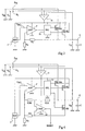
- Figure 1 shows a classic diagram of a regulator intended to supply a voltage regulated to a specified value from a single supply voltage.
- Such a regulator receives, on an input terminal E, a supply voltage to be regulated V, and delivers, on an output terminal S, a regulated voltage V R.
- the regulator comprises a circuit 1 providing a reference voltage, and a circuit 2 for controlling a P-channel power MOS transistor M10, the source of which is connected to terminal E and the drain of which constitutes terminal S.
- Circuit 1 has the role of setting a precise reference voltage V BG to control, via the control circuit 2, the output voltage V R.
- Circuit 1 comprises two bipolar PNP type transistors Q1 and Q2, the respective transmitters of which are connected to terminal E and the respective collectors of which constitute two output terminals 3, 4 of circuit 1 intended to control circuit 2 as will be seen by the following.
- the bases of the transistors Q1 and Q2 are connected to the collector of the transistor Q1.
- the collectors of the transistors Q1 and Q2 are respectively connected to the collectors of bipolar transistors of the NPN type Q3 and Q4, the bases of which are connected and constitute a terminal 5 at the reference potential V BG .
- the emitter of transistor Q4 is connected to ground via two resistors R1 and R2 connected in series.
- the emitter of transistor Q3 is connected to the midpoint of the series association of resistors R1 and R2.
- the resistors R1 and R2 and the surface ratio of the transistors Q3 and Q4 are chosen to obtain the desired voltage V BG with a given current in the transistors Q1, Q2, Q3 and Q4.
- Circuit 1 includes a starting circuit consisting of a current source I, the output of which is connected to ground via a diode D and at the base of a bipolar transistor of NPN type Q D , the collector of which is connected to terminal 4 and whose transmitter is connected to the midpoint of the series association of resistors R1 and R2.
- Circuit 1 shown in Figure 1 is generally designated by its Anglo-Saxon name "band gap” and its operation is perfectly known.
- the circuit 2 for controlling the transistor M10 consists of two bipolar PNP transistors of the Q5 and Q6 type, the respective emitters of which are connected to the terminal E and the bases of which are respectively connected to the terminals 4 and 3.
- the collectors of the transistors Q5 and Q6 are connected to the respective drains of two N-channel MOS transistors M11 and M3 mounted in current mirror, the sources of the transistors M11 and M3 being connected to ground and the transistor M11 being mounted as a diode.
- the collector of transistor Q6 constitutes an output terminal of circuit 2 connected to the gate of transistor M10.
- a resistive bridge consisting of resistors R3 and R4 is generally connected between terminal S and ground when the desired voltage V R is different from the reference voltage V BG .
- This divider bridge is connected to terminal 5 of circuit 1 to form a feedback loop making it possible to maintain the reference voltage V BG on the bases of the transistors Q3 and Q4.
- This reference voltage ensures the equality of the currents in the transistors Q3 and Q4.
- This current imbalance is amplified by circuit 2 and modifies the potential V G for controlling the transistor M10 to restore, via the resistive bridge R3-R4, the voltage V BG which ensures the equality of the currents in the transistors Q3 and Q4.
- the voltage V R is equal to V BG (R3 + R4) / R4.
- a capacitor C is generally provided at the outlet of the regulator and is connected between terminal S and earth. The role of this capacitor is, in particular, to ensure the stability of the feedback loop.
- a drawback of a regulator as shown in FIG. 1 is that, if the voltage V becomes lower than the regulated voltage V R , the terminals E and S are short-circuited by the transistor M10.
- the substrate of the MOS transistor M10 or its well is generally connected to its source, that is to say to the potential V.
- the substrate of a MOS transistor or its well is generally designated by the "body” of the transistor ("bulk” in its Anglo-Saxon name) to distinguish it from the overall substrate of the integrated circuit on which the various components are made.
- the body of a MOS transistor is generally symbolized by an arrow whose direction indicates the P or N type of the transistor channel.
- the PN junction between the drain and the body of the transistor M10 is directly biased and the transistor is then short-circuited by the drain / body diode.
- the drain and the source of the transistor M10 are exchanged (the current being reversed), which transforms the feedback from the circuit 1 into reaction.
- This short circuit harms a second role of the capacitor C which is to temporarily supply the load in the event of insufficient or disappearance of the supply voltage V.
- the regulator when used to supply a microprocessor, one seeks to be able to maintain the supply of the microprocessor while it can save the data, following an insufficiency or the disappearance of the supply voltage.
- the voltage V R is generally compared with respect to a threshold by means of a circuit external to the regulator to detect a decrease in the voltage V R and then use the capacitor C to temporarily supply the microprocessor before the voltage V R disappears.
- a drawback of such a solution is that it introduces a voltage drop of about 0.7 volts between the input and output terminals of the regulator.
- Isolation diodes are also used when we want to be able to power the regulator as shown in FIG. 1 from different voltages by selecting, as the voltage to be regulated, the one with the greatest potential Student.
- FIG. 2 represents a classic example of a voltage regulator automatically selecting, from two supply voltages V M and V L arriving at two input terminals E M and E L , the highest voltage.
- the circuits 1 and 2 represented in FIG. 1 have been shown diagrammatically in FIG. 2 by a reference voltage source 1 and by an amplifier 2 receiving, as input, the reference voltage V BG and the potential of the midpoint of the resistive divider bridge R3-R4.
- Amplifier 2 and generator 1 are polarized by the highest supply voltage V M or V L by means of diodes, respectively D1, D2 and D3, D4 interposed in series between each terminal E M or E L and the generator 1 or amplifier 2 bias terminal.
- MOS transistors suitably ordered and which fulfill the same function of selecting the highest voltage and voltage isolation function the weakest. These transistors, like the diodes, introduce an additional voltage drop.
- Document EP-A-0465933 describes a voltage regulator suitable for being supplied from several independent voltages each other.
- a voltage amplifier proportional to an error voltage between the regulated voltage and a reference voltage drives a bipolar transistor multi-transmitters with each transmitter connected to a voltage feed.
- a first drawback of this regulator is that it leads to a high consumption when the most tension high supply voltages is less than the voltage of regulated output desired. Indeed, the amplifier then seeks maintain the output voltage at the desired value and the bipolar transistor conducts strongly.
- Another disadvantage is than the supply terminals associated with the highest voltages weak are not isolated from the rest of the circuit if they are at least 0.7 volts higher than the voltage of control of the multi-emitter transistor.
- the present invention aims to propose a new regulator voltage suitable for selecting a supply voltage highest among at least two independent voltages while minimizing the voltage drop across the regulator.
- the present invention also aims to optimize the use a decoupling capacitor placed at the output of the regulator to temporarily supply the load when no voltage unregulated supply is no more than the voltage of regulated output.
- the present invention provides a voltage regulator intended to control a voltage of output delivered by a power transistor on a voltage of reference, and comprising at least two input terminals specific to each receiving an independent supply voltage; a means for automatically selecting the supply voltage the highest among the voltages present at the input terminals; and a means for isolating the supply terminal associated with the lowest voltage of the rest of the circuit, said means introducing a very low voltage drop, corresponding to that of a single power transistor, between the input terminal at the highest voltage and one regulator output terminal.
- the regulator comprises at least two first transistors of power each having a first power electrode connected directly to one of said input terminals and a second power electrode connected to the output terminal, and a control circuit suitable for making that of the said conductive power transistors which is associated with the supply voltage the highest and block the other power transistor.
- At least said first two associated power transistors the supply voltages present at the input terminals of the regulator are P-channel MOS transistors, the regulator comprising a circuit for polarizing the bodies of at least the said first two power transistors at the highest voltage.
- said selection means selects the voltage supply of the regulator circuits among the voltages on the input terminals and a voltage regulated output present on the output terminal.
- FIG. 3 represents a first embodiment of a voltage regulator according to the invention.
- This regulator comprises two input terminals E M and E L , suitable for receiving respectively supply voltages V M and V L independent of each other, and an output terminal S, associated with a decoupling capacitor C and delivering a regulated voltage V R.
- the regulator comprises two P-channel power MOS transistors M10M and M10L having respectively a first power electrode connected to the terminal E M or E L and a second power electrode connected to the terminal S.
- a circuit 1 ' provides a reference voltage V BG on which the output voltage V R must be controlled, and is associated with an amplifier 2'.
- a resistive divider bridge made up of resistors R3 and R4 is connected in series between terminal S and ground.
- the midpoint of the association of resistors R3 and R4 is connected to a first input of the amplifier 2 ', a second input of which receives the voltage V BG .
- the amplifier 2 ′ is associated with a circuit 10 for selecting the power transistor M10M or M10L to be controlled.
- a characteristic of the present invention is that the circuits 1 ′, 2 ′ and 10 are supplied by the highest voltage among the voltages V L , V M and V R by means of a comparator 11 of which three inputs are respectively connected to the terminals E L , E M and S.
- Another characteristic of the present invention is that the bodies (substrates or boxes) of the MOS transistors M10M and M10L are connected to the highest potential among the voltages V M , V L and V R.
- This connection has been symbolized in FIG. 3 by a connection between the bodies of the transistors M10M and M10L and the output of the comparator 11.
- the transistors M10M and M10L are not conductive insofar as their respective bodies are also at the voltage V R , which prohibits any direct polarization of the drain / body and source / body junctions.
- the transistor M10L or M10M associated with the lower supply voltage V L or V M is blocked by the circuit 10 and , even if this lowest voltage V L or V M is lower than the voltage V R , this transistor is not conductive insofar as its body is brought to the highest potential.
- An advantage of the present invention is that the lowest voltage V M or V L is isolated from the regulator.
- Another advantage of the present invention is that the voltage drop between regulator input and output terminals is weak. Indeed, it is limited to about 0.1 volts corresponding to the voltage drop in one of the MOS transistors of power in the on state.
- Another advantage of the first embodiment is that, even if the reference potential V BG is no longer maintained when the two voltages V L and V M are insufficient or disappear, an optimal use of the capacitor C is guaranteed to temporarily supply the charge.
- FIG. 4 represents a second embodiment of the present invention, in which the regulator further comprises a comparator 12 associated with a low power P channel transistor M10R for generating a RESET logic signal.
- This RESET signal is intended to indicate a regulator supply fault by means of one of the voltages V M or V L , that is to say that the highest voltage of the regulator is the voltage V R , and that the output voltage V R is less than a determined threshold.
- This RESET signal is, for example, used to signal to the load (not shown), for example a microprocessor, that the voltage which it receives is now only supplied by the capacitor C and is therefore only temporary.
- the transistor M10R is connected, by its source, to the terminal S and, by its drain, to a first input terminal of the comparator 12 as well as, via a resistor R5, at the midpoint of the series association of resistors R3A and R3B with resistance R4.
- the gate of the transistor M10R is connected to the selection circuit 10 which therefore selects the transistor to be made conductive from the three transistors M10M, M10L and M10R as a function of which of the three voltages V M , V L and V R is the highest.
- the tipping point of comparator 12 is fixed by the values of resistors R3A, R3B, R4 and R5. Its value corresponds to: V BG . [(R5 / R4). (R3A + R3B) / (R5 + R3B) + 1].
- An advantage of this second embodiment is that the transistor M10R makes it possible to maintain the feedback loop even when the voltage V R is the highest voltage, thus allowing the regulator to integrate the generation of a RESET signal when the voltage V R corresponds to the discharge of the capacitor C and becomes less than a threshold voltage. This makes it possible to determine this threshold voltage very precisely insofar as it is linked to the voltage V BG fixed by the circuit 1 '. In addition, this minimizes the consumption linked to the generation of the RESET signal insofar as the components of the regulator are used which are generally chosen for their low consumption.
- means for selecting the voltage higher are provided separately for the circuit 1 ', circuits 2' and 10 and for the polarization of the bodies of M10M and M10L transistors.
- a bias circuit is provided bodies intended for M10M and M10L transistors as well than other regulator P-channel MOS transistors.
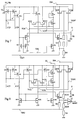
- FIG. 5 represents an embodiment of the circuit 1 'for generating the reference voltage V BG , as well as the control circuit 2' and the selection circuit 10 associated therewith.
- FIG. 6 represents an embodiment of a circuit 13 for biasing the bodies of the P-channel MOS transistors, as well as the transistors M10L, M10M and M10R and the resistive means 14 associated with the comparator 12 and the feedback of the regulator .
- the circuit 1 ' consists of a current source I, a diode D, resistors R1 and R2, and transistors Q D , Q3 and Q4 as described above in relation to FIG. 1.
- the transistors Q1 and Q2 of FIG. 1 are, for example, each replaced by three bipolar PNP type transistors respectively associated with the terminals E M , E L and S or, as shown, by two multi-emitter transistors whose respective collectors are connected to the collectors of the transistors Q3 and Q4 and respectively define the output terminals 3 and 4 of the circuit 1 '.
- a first transmitter, respectively Q1M or Q2M, of the multi-transmitter transistors is connected to the terminal E M
- a second transmitter, respectively Q1L or Q2L is connected to the terminal E L
- a third transmitter, respectively Q1R or Q2R is connected to terminal S.
- the operation of circuit 1 ' is similar to that of circuit 1 exposed in relation to FIG. 1 with the difference that its supply voltage is always the highest voltage among the voltages V M , V L and V R.
- Terminal 4 is connected to the respective bases of three bipolar PNP transistors Q5M, Q5R and Q5L of circuit 2 'whose emitters are respectively connected to terminals E M , S and E L.
- the respective collectors of the transistors Q5M, Q5R and Q5L are connected to the drains and grids of N-channel MOS transistors M11M, M11R and M11L mounted as a diode and the respective sources of which are connected to ground.
- N-channel MOS transistors M3L, M3R and M3M whose respective sources are connected to ground, are mounted as current sources on the transistors M11L, M11R and M11M with which they constitute current mirrors by connection of their respective gates .
- the respective drains of the transistors M3L and M3M are connected, via an N-channel MOS transistor M4L, M4M, the gate of which is connected to the respective M3L or M3M transistor, to the collector of a bipolar PNP transistor Q6L, Q6M (or to the common collector of a multi-emitter transistor).
- the drain of the transistor M3R is directly connected to the collectors of the transistors Q6L and Q6M.
- the respective drains of the transistors M3L and M3M are also connected to the collector of a bipolar transistor of PNP type, respectively Q6RA or Q6RB, the emitter of which is connected to the terminal S.
- the respective bases of the transistors Q6RA, Q6RB, Q6L and Q6M are connected to terminal 3.
- the collectors of the transistors Q6RA and Q6RB deliver, respectively, control potentials V GL and V GM on the gates of the transistors M10L and M10M (FIG. 6).
- the collector of the multi-emitter transistor Q6L-Q6M delivers a control potential V GR on the gate of the transistor M10R ( Figure 6).
- circuit 2 The operation of circuit 2 'described above is deduced from that of circuit 2 of FIG. 1 with regard to the transistors Q5, Q6, M3 and M11 assigned the respective letters M, R and L, the higher of the voltages V M , V L , V R causing the transistors Q5, Q6, M3 and M11 to carry the corresponding letter and blocking the other transistors.
- the circuit 10 comprises two P-channel MOS transistors M12L and M12M connected in series between the respective collectors of the transistors Q6RA and Q6RB.
- the common electrode of the transistors M12L and M12M is connected to the common collector of the transistors Q6L and Q6M.
- the role of the transistors M12L and M12M is to block the two power transistors among the transistors M10L, M10M and M10R which are associated with the two lowest voltages among the voltages V M , V L and V R.
- Two P-channel MOS transistors M14 and M15 are connected in series and in a diode between a terminal V B and the common gates of the transistors M12L and M12M.
- the terminal V B represents the output terminal of the circuit 13 for biasing the bodies of the P channel transistors which will be described hereinafter in relation to FIG. 6.
- the terminal V B is at the potential of the highest voltage among the voltages V M , V L and V R.
- the drain of transistor M15 is connected to the common drain of three N-channel MOS transistors M13L, M13R and M13M which are mounted as a current mirror on the respective transistors M11L, M11R and M11M.
- circuits 2 ′ and 10 will be better understood in relation to FIGS. 7 and 8.
- the circuit 13 for biasing the bodies of the P-channel transistors, in particular the M10L and M10M transistors, at the highest voltage among the voltages V M , V L and V R comprises three similar arrangements each consisting of three P-channel MOS transistors and an N-channel MOS transistor.
- Each group of four transistors comprises a P-channel transistor, M16M, M16R or M16L, respectively, connected between the terminal E M , S or E L and the terminal V B.
- the respective gates of the transistors M16M, M16R and M16L are connected to the source of the N-channel MOS transistor M9M, M9R and M9L of the corresponding group.
- the transistors M9M, M9R and M9L are mounted as a current mirror on the respective transistors M11M, M11R and M11L (FIG. 5).
- the respective gates of the transistors M11M, M11R and M11L have been designated by terminals V BM , V BR and V BL to allow the transfer of the connections between FIGS. 5 and 6.
- the two other MOS channel transistors P, respectively M7M and M8M, M7R and M8R, M7L and M8L, of each group of the circuit 13 have a first electrode connected to the terminal, respectively E M , S or E L , their gates being connected to the drain of the transistor M9 of the group corresponding.
- a second electrode of the transistors M7M and M7R is connected to the drain of the transistor M9L.
- a second electrode of the transistors M8L and M8R is connected to the drain of the transistor M9M.
- a second electrode of the transistor M7L and M8M is connected to the drain of the transistor M9R.
- the transistor M16 of the corresponding group establishes the potential of the terminal V B at the highest voltage and the transistors M7 and M8 of this group block the six P-channel MOS transistors of the other two groups by bringing their respective gates to the most potential Student. All the bodies of the P channel transistors of the circuit 13 are connected to the terminal V B to prevent any short circuit by the drain / body or source / body diodes.
- the polarization of the bodies of P-channel transistors, at the highest voltage among the voltages V M , V L and V R is achieved by means of a bipolar transistor of PNP type with three emitters.
- Each transmitter is connected to one of the voltages V M , V L , V R (in a similar way to the transmitters Q2R, Q2L and Q2M of the circuit 1 ') and the base of this transistor is biased by a current source of low value (approximately 1 ⁇ A), made from circuit 1 '.
- the collector of this transistor is connected to the bodies of the P-channel transistors to be polarized. The collector then takes the potential of the transmitter which is connected to the highest voltage, thus polarizing the bodies of the P-channel transistors at this same voltage.
- the comparator 12 responsible for producing the RESET signal is biased by being connected to the terminal V B.
- This comparator 12 having a very low consumption, the potential of the terminal V B is not substantially modified.
- the comparator 12 can also be powered only by the voltage V R. Indeed, when generating the RESET logic signal, the highest voltage will always be the voltage V R.
- FIG. 7 illustrates the operation of the voltage regulator according to the present invention when the highest voltage of the circuit corresponds to one of the supply voltages V M and V L. The operation is similar regardless of the higher voltage V M or V L.
- FIG. 7 corresponds to normal operation of the regulator where the regulated voltage V R is produced from the voltage V L.
- the blocked transistors which do not intervene in the operation have been eliminated, and the terminals V B and E L have been confused.
- Circuit 1 has only been partially shown.
- the transistor Q6L is found in series with the transistor M12L, the gate of which is biased by the transistors M14 and M15, and with the transistor M3L.
- the transistor Q6L associated with the transistor M12L therefore constitutes a cascode current source charged by the transistor M3L, which is controlled by the transistors Q2L, Q5L and M11L, and whose output V GL is connected to the gate of the transistor M10L.
- the operation described in relation to FIG. 1 is thus reproduced.
- the potential of the gates of the transistors M12L and M12M is substantially equal to V L - 2V TH , where V TH represents the threshold voltage of the transistors M14 and M15.
- the potential V GR present on the source of the transistor M12L is therefore substantially equal to V L - 2V TH , increased by the gate-source voltage drop of the transistor M12L.
- This voltage drop is equal to the threshold voltage V TH of the transistor M12L plus a term due to the drain-source current of the transistor M12L and corresponding to the parabolic component of its gate-source voltage.
- the potential V GR is greater than V L - V TH .
- the potential V GM is, by the same reasoning, equal to the potential V GR , the transistor M12M being conductive but not crossed by any current.
- V GR V GM > V L - V TH
- the transistors M10R and M10M are blocked because their respective sources are at potentials lower than the voltage V L. Blocking the transistor M10M isolates the power supply V M , while blocking the transistor M10R causes the resistance of the feedback loop to correspond to the resistance R3 (R3A + R3B).
- the output voltage V R is equal to V BG . (R3 + R4) / R4. It will be noted that, as the body of the transistor M10M is connected to the potential V L , the terminal E M is well completely isolated from the regulator and there is no short circuit between the terminals E M and S.
- the potential difference between the source and the drain of the transistor M10L is too small to supply sufficient current to the load connected to the terminal S.
- the loop feedback consisting of resistors R3A and R3B, transistor Q3 (not shown in Figure 6), transistor Q6L and transistor M12L, then lowers the potential V GL to a value near ground.
- the transistor M3L then operates in triode, which unlocks the transistor M4L.
- the unlocking of the transistor M4L leads to the conduction of the transistor M10R which then short-circuits the resistors R3A and R3B.
- the voltage V R cannot in this case be maintained at the desired nominal value and decreases.
- the feedback loop continues to operate by the transistor M10R and the resistor R5, which guarantees that the voltage V BG is maintained at the chosen reference value.
- the regulator When the voltage V L becomes lower than the voltage V R or disappears, the regulator is then in an operating mode where it is supplied by the voltage V R and where it is capable of generating the RESET signal which will be described later in relation to figure 8.
- FIG. 8 does not represent the transistors of FIGS. 5 and 6 which are blocked and which do not intervene in the operation. In the case shown in FIG. 8, it is considered that the voltage V R is greater than the voltages V L and V M.
- the two transistors Q6RA and Q6RB have their base-emitter junctions in parallel and their currents are therefore equal.
- a current flows here in the two transistors M12L and M12M, we obtain as before, from a functional point of view, a source of current cascode.
- the upper part (Q6RA, M12L and Q6RB, M12M) is here divided into two and produces, on the respective sources of the transistors M12L and M12M, the two blocking voltages V GL and V GM which are both greater than V R - V TH .
- the transistors M10M and M10L are therefore blocked and, as their respective bodies are at potential V R , the terminals E M and E L are completely isolated from the regulator.
- the lower part (M12L, M12M and M3R) of the cascode current source supplies the voltage V GR , determined by the feedback loop comprising the transistor M10R and the resistor R5.
- V BG is well maintained at the specified value.
- the voltage V BG is then used to index the threshold from which the RESET signal is produced by means of the comparator 12.
- the switching of the comparator 12 occurs when the voltage V R becomes lower than V BG . [(R5 /R4).(R3A + R3B) / (R5 + R3B) + 1].
- all the bodies of the N-channel MOS transistors are connected to their source.
- all the bodies of the P-channel MOS transistors of circuit 13 as well as the bodies of the transistors M12L and M12M and the power transistors M10L and M10M are connected to the terminal V B at the potential of the highest voltage.
- the body of transistor M14 is also connected to voltage V B as its source, and the bodies of transistors M10R and M15 are connected to their respective sources.
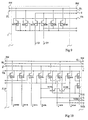
- Figures 9 and 10 illustrate another embodiment according to which the upper transistors of circuits 1 ′, 2 'and 10 are P-channel MOS transistors. In FIGS. 9 and 10, only the upper parts of circuits 1 ', 2' and 10 have been represented.
- the transistors Q1R, Q1L and Q1M are replaced, respectively, by P-channel MOS transistors M1M, M1L and M1R (FIG. 9).
- the transistors Q2M, Q2L and Q2R are replaced, respectively, by transistors M2M, M2L and M2R.
- the bodies of these P channel MOS transistors are all connected to the terminal V B to guarantee the isolation between the voltages V M , V L and V R.
- the bipolar transistors of circuit 2 ′ are replaced by P-channel MOS transistors whose references in FIG. 10 are similar by replacing the letter Q with the letter M. All the bodies of these P-channel MOS transistors are then connected to the terminal V B.
- the present invention is capable of various variants and modifications which will appear to the man of art.
- the sizing of the transistors and resistance is within the reach of the skilled person in function desired functional characteristics.
- the regulator according to the invention can be fully realized in bipolar technology by replacing P channel MOS transistors by PNP transistors and N-channel MOS transistors by NPN transistors. In this case, it is not necessary to provide a bias circuit 13 bodies of P-channel MOS transistors.
- MOS transistors constitute an embodiment preferred according to the invention insofar as they are controllable in voltage, which results in lower consumption of the regulator.
- the invention also applies to the realization of a negative voltage regulator. It is enough to do this, replace the P-channel MOS transistors with N channel transistors and vice versa, and replace the PNP-type bipolar transistors by type-transistors NPN and vice versa. The voltage selection is then made on the voltage with the most negative value.
Landscapes
- Engineering & Computer Science (AREA)
- Physics & Mathematics (AREA)
- Electromagnetism (AREA)
- General Physics & Mathematics (AREA)
- Radar, Positioning & Navigation (AREA)
- Automation & Control Theory (AREA)
- Continuous-Control Power Sources That Use Transistors (AREA)
Claims (4)
- Spannungsregler zur Regelung einer von einem Leistungstransistor (M10M, M10L) gelieferten Ausgangsspannung (VR) in Abhängigkeit von einer Bezugsspannung (VBG),
dadurch gekennzeichnet , daß der Regler umfaßt :wenigstens zwei Eingangsanschlüsse (EM , EL), denen jeweils eine unabhängige Speisespannung (VM, VL) zugeführt werden kann;ein Mittel (11), um unter den an den Eingangsanschlüssen (EM, EL) anliegenden Spannungen automatisch die höchste Speisespannung (VM, VL) auszuwählen;ein Mittel, um den der niedrigsten Spannung (VM, VL) zugeordneten Eingangsanschluß (EM,EL) von der übrigen Schaltung zu trennen, wobei diese Mittel einen sehr niedrigen Spannungsabfall entsprechend dem Spannungsabfall eines einzigen Leistungstransistors zwischen dem Eingangsanschluß (EM,EL) mit der höchsten Spannung (VM, VL) und einem Ausgangsanschluß (S) des Reglers einführen. - Spannungsregler nach Anspruch 1, dadurch gekennzeichnet, daß der Regler umfaßt:wenigstens zwei erste Leistungstransistoren (M10M, M10L), die jeder jeweils eine direkt mit einem der genannten Eingangsanschlüsse verbundene erste Leistungselektrode und eine mit dem Ausgangsanschluß (S) verbundene zweite Leistungselektrode aufweisen; sowieeine Steuerschaltung (10), welche den der höchsten Speisespannung (VM, VL) zugeordneten Leistungstransistor (M10M, M10L) in den leitenden Zustand überführt und den anderen Leistungstransistor (M10M, M10L) sperrt.
- Spannungsregler nach Anspruch 2, dadurch gekennzeichnet, daß wenigstens die beiden ersten Leistungstransistoren (M10M, M10L), welche den an den Eingangsanschlüssen (EM, EL) anliegenden Speisespannungen (VM, VL) zugeordnet sind, P-Kanal-MOS-Transistoren sind, und daß der Regler eine Schaltung (13) aufweist, um die Bulk-Körper wenigstens der genannten beiden ersten Leistungstransistoren (M10M, M10L) mit der höchsten Spannung (VM, VL, VR) vorzuspannen.
- Spannungsregler nach einem der Ansprüche 1 bis 3, welcher einen Kondensator (C) zwischen dem Ausgangsanschluß (S) und Masse aufweist, dadurch gekennzeichnet, daß die genannten Wählmittel (11) die Speisespannungen der Schaltungen des Reglers unter den an den Eingangsanschlüssen (EM, EL) anliegenden Speisespannungen (VM, VL) und einer an dem Ausgangsanschluß (S) vorliegenden geregelten Ausgangsspannung (VR) auswählt.
Applications Claiming Priority (2)
| Application Number | Priority Date | Filing Date | Title |
|---|---|---|---|
| FR9613280A FR2755316B1 (fr) | 1996-10-25 | 1996-10-25 | Regulateur de tension a selection automatique d'une tension d'alimentation la plus elevee |
| FR9613280 | 1996-10-25 |
Publications (2)
| Publication Number | Publication Date |
|---|---|
| EP0838745A1 EP0838745A1 (de) | 1998-04-29 |
| EP0838745B1 true EP0838745B1 (de) | 2001-12-12 |
Family
ID=9497197
Family Applications (1)
| Application Number | Title | Priority Date | Filing Date |
|---|---|---|---|
| EP97410120A Expired - Lifetime EP0838745B1 (de) | 1996-10-25 | 1997-10-24 | Spannungsregler mit automatischer Auswahl der höchsten Versorgungsspannung |
Country Status (4)
| Country | Link |
|---|---|
| US (1) | US6002295A (de) |
| EP (1) | EP0838745B1 (de) |
| DE (1) | DE69709029D1 (de) |
| FR (1) | FR2755316B1 (de) |
Families Citing this family (31)
| Publication number | Priority date | Publication date | Assignee | Title |
|---|---|---|---|---|
| FR2798014B1 (fr) | 1999-08-31 | 2002-03-29 | St Microelectronics Sa | Circuit d'alimentation a selecteur de tension |
| JP3540231B2 (ja) * | 2000-01-31 | 2004-07-07 | 沖電気工業株式会社 | クランプ回路及び非接触式通信用インターフェース回路 |
| JP3696470B2 (ja) * | 2000-02-22 | 2005-09-21 | 富士通株式会社 | Dc−dc変換回路、電源選択回路、および機器装置 |
| US6686789B2 (en) * | 2002-03-28 | 2004-02-03 | Agere Systems, Inc. | Dynamic low power reference circuit |
| US6642750B1 (en) * | 2002-04-15 | 2003-11-04 | International Business Machines Corporation | Sequencing circuit for applying a highest voltage source to a chip |
| US6897715B2 (en) * | 2002-05-30 | 2005-05-24 | Analog Devices, Inc. | Multimode voltage regulator |
| US6819165B2 (en) * | 2002-05-30 | 2004-11-16 | Analog Devices, Inc. | Voltage regulator with dynamically boosted bias current |
| US6744151B2 (en) * | 2002-09-13 | 2004-06-01 | Analog Devices, Inc. | Multi-channel power supply selector |
| US6815998B1 (en) * | 2002-10-22 | 2004-11-09 | Xilinx, Inc. | Adjustable-ratio global read-back voltage generator |
| US20040124909A1 (en) * | 2002-12-31 | 2004-07-01 | Haider Nazar Syed | Arrangements providing safe component biasing |
| US6753722B1 (en) * | 2003-01-30 | 2004-06-22 | Xilinx, Inc. | Method and apparatus for voltage regulation within an integrated circuit |
| TWI293464B (en) * | 2003-07-08 | 2008-02-11 | Winbond Electronics Corp | Two phase internal voltage generator |
| US6995599B2 (en) * | 2003-08-26 | 2006-02-07 | Texas Instruments Incorporated | Cross-conduction blocked power selection comparison/control circuitry with NTC (negative temperature coefficient) trip voltage |
| DE102004022425B4 (de) * | 2004-05-06 | 2006-12-28 | Infineon Technologies Ag | Integrierte Schaltungsanordnung zur Stabilisierung einer Spannung |
| US7675282B2 (en) | 2006-10-10 | 2010-03-09 | Infineon Technologies Ag | Dual mode chip card voltage regulation circuit and method |
| TW200828224A (en) * | 2006-12-29 | 2008-07-01 | Innolux Display Corp | Liquid crystal display |
| US7586357B2 (en) * | 2007-01-12 | 2009-09-08 | Texas Instruments Incorporated | Systems for providing a constant resistance |
| FR2916288B1 (fr) * | 2007-05-18 | 2009-08-21 | Commissariat Energie Atomique | Dispositif d'alimentation d'un circuit electronique et circuit electronique |
| KR101286241B1 (ko) * | 2007-11-26 | 2013-07-15 | 삼성전자주식회사 | 최대 전압 선택회로 |
| CN101465559A (zh) * | 2007-12-19 | 2009-06-24 | 鸿富锦精密工业(深圳)有限公司 | 双重电源转换电路 |
| EP2180392A1 (de) * | 2008-10-22 | 2010-04-28 | Micronas GmbH | Elektrische Spannungsversorgung |
| CN102545293B (zh) * | 2010-12-29 | 2016-03-23 | 华润矽威科技(上海)有限公司 | 低成本带电平补偿的多路电压信号自动选高电路 |
| US9329649B2 (en) * | 2012-11-21 | 2016-05-03 | Stmicroelectronics S.R.L. | Dual input single output regulator for an inertial sensor |
| JP6441619B2 (ja) | 2014-09-03 | 2018-12-19 | ルネサスエレクトロニクス株式会社 | 半導体装置 |
| KR102365143B1 (ko) | 2015-09-22 | 2022-02-18 | 삼성전자주식회사 | 멀티-파워와 게인-부스팅 기술을 이용하는 전압 레귤레이터와 이를 포함하는 모바일 장치들 |
| EP3208748B1 (de) * | 2016-02-19 | 2019-06-12 | Nxp B.V. | Stromschaltkreis |
| FR3051570B1 (fr) * | 2016-05-23 | 2019-11-22 | STMicroelectronics (Alps) SAS | Dispositif de regulation a faible chute de tension, en particulier capable de supporter des tensions d'alimentation compatibles avec la norme usb type c |
| US11599133B2 (en) * | 2021-07-13 | 2023-03-07 | Globalfoundries U.S. Inc. | Power supply with integrated voltage regulator and current limiter and method |
| EP4235500B1 (de) * | 2022-02-25 | 2025-03-26 | STMicroelectronics razvoj polprevodnikov d.o.o. | Ic-kartenregler |
| CN116661535A (zh) * | 2022-02-25 | 2023-08-29 | 意法半导体发展有限责任公司 | Ic卡调节器 |
| US20250021121A1 (en) * | 2023-07-10 | 2025-01-16 | Apple Inc. | Voltage Regulator with Voltage Rail Switching |
Family Cites Families (10)
| Publication number | Priority date | Publication date | Assignee | Title |
|---|---|---|---|---|
| US4617473A (en) * | 1984-01-03 | 1986-10-14 | Intersil, Inc. | CMOS backup power switching circuit |
| US4686388A (en) * | 1985-03-12 | 1987-08-11 | Pitney Bowes Inc. | Integrated circuit substrate bias selection circuit |
| JPS63245236A (ja) * | 1987-03-31 | 1988-10-12 | 株式会社東芝 | 電源切替回路 |
| US4779037A (en) * | 1987-11-17 | 1988-10-18 | National Semiconductor Corporation | Dual input low dropout voltage regulator |
| JP2733796B2 (ja) * | 1990-02-13 | 1998-03-30 | セイコーインスツルメンツ株式会社 | スイッチ回路 |
| US5103157A (en) * | 1990-07-10 | 1992-04-07 | National Semiconductor Corp. | Common emitter amplifiers operating from a multiplicity of power supplies |
| JP2973063B2 (ja) * | 1992-10-27 | 1999-11-08 | セイコーインスツルメンツ株式会社 | スイッチ回路 |
| US5341034A (en) * | 1993-02-11 | 1994-08-23 | Benchmarq Microelectronics, Inc. | Backup battery power controller having channel regions of transistors being biased by power supply or battery |
| FR2735927B1 (fr) * | 1995-06-21 | 1997-08-01 | Sgs Thomson Microelectronics | Circuit de commutation permettant de fournir selectivement des tensions de signes differents |
| US5748033A (en) * | 1996-03-26 | 1998-05-05 | Intel Corporation | Differential power bus comparator |
-
1996
- 1996-10-25 FR FR9613280A patent/FR2755316B1/fr not_active Expired - Fee Related
-
1997
- 1997-10-21 US US08/955,211 patent/US6002295A/en not_active Expired - Lifetime
- 1997-10-24 DE DE69709029T patent/DE69709029D1/de not_active Expired - Lifetime
- 1997-10-24 EP EP97410120A patent/EP0838745B1/de not_active Expired - Lifetime
Also Published As
| Publication number | Publication date |
|---|---|
| FR2755316A1 (fr) | 1998-04-30 |
| EP0838745A1 (de) | 1998-04-29 |
| US6002295A (en) | 1999-12-14 |
| DE69709029D1 (de) | 2002-01-24 |
| FR2755316B1 (fr) | 1999-01-15 |
Similar Documents
| Publication | Publication Date | Title |
|---|---|---|
| EP0838745A1 (de) | Spannungsregler mit automatischer Auswahl der höchsten Versorgungsspannung | |
| EP0388329B1 (de) | Steuerschaltung für einen MOS-Leistungstransistor mit induktiver Last | |
| EP1093044B1 (de) | Linearer Regler mit niedrigem seriellen Spannungsabfall | |
| FR2637703A1 (fr) | Circuit regulateur stabilise a faible tension de mise hors fonction | |
| FR2830091A1 (fr) | Regulateur de tension incorporant une resistance de stabilisation et un circuit de limitation du courant de sortie | |
| EP1326154B1 (de) | Ladungspumpe mit sehr grossem Ausgangsspannungsbereich | |
| EP0788047B1 (de) | Vorrichtung zur Erzeugung von Referenzstrom in einer integrierten Schaltung | |
| EP0649079B1 (de) | Geregelter Spannungsquellengenerator der Bandgapbauart | |
| EP0432058A1 (de) | Dynamische Isolierschaltung für integrierte Schaltungen | |
| FR2566146A1 (fr) | Circuit de reference de tension de bande interdite perfectionne | |
| EP0838746B1 (de) | Spannungsregler | |
| EP1380913A1 (de) | Linearer Spannungsregler | |
| FR2738424A1 (fr) | Interrupteur analogique basse tension | |
| EP1073202B1 (de) | Steuerschaltung für einen Pegelumsetzer-Hochspannungsschalter | |
| EP0159233A1 (de) | Steuerschaltung zum Schalten eines Leistungstransistors | |
| EP0690573B1 (de) | Steuerschaltung für den teilweisen Standby-Betrieb einer Vorspannungsquelle | |
| FR2809834A1 (fr) | Source de courant a faible tension d'alimentation et a faible sensibilite en tension | |
| EP0717333B1 (de) | Speisespannung-Auswahlschaltung für Spannungsregler | |
| EP0219158A1 (de) | Spannungsregelungsschaltung | |
| EP1102148B1 (de) | Niedrigtemperaturkorrigierte Spannungsgeneratoreinrichtung | |
| FR2733101A1 (fr) | Circuit logique de type a emetteurs couples, fonctionnant sous une faible tension d'alimentation | |
| FR2677771A1 (fr) | Circuit de detection de niveau de polarisation inverse dans un dispositif de memoire a semiconducteurs. | |
| FR2881850A1 (fr) | Circuit de generation d'une tension de reference flottante, en technologie cmos | |
| EP0331253B1 (de) | Stromquelle mit einem breiten Bereich an Ausgangsspannungen | |
| EP4517473A1 (de) | Spannungsregler |
Legal Events
| Date | Code | Title | Description |
|---|---|---|---|
| PUAI | Public reference made under article 153(3) epc to a published international application that has entered the european phase |
Free format text: ORIGINAL CODE: 0009012 |
|
| AK | Designated contracting states |
Kind code of ref document: A1 Designated state(s): DE FR GB IT |
|
| 17P | Request for examination filed |
Effective date: 19981012 |
|
| AKX | Designation fees paid |
Free format text: DE FR GB IT |
|
| RBV | Designated contracting states (corrected) |
Designated state(s): DE FR GB IT |
|
| RAP3 | Party data changed (applicant data changed or rights of an application transferred) |
Owner name: STMICROELECTRONICS S.A. |
|
| 17Q | First examination report despatched |
Effective date: 20001026 |
|
| GRAG | Despatch of communication of intention to grant |
Free format text: ORIGINAL CODE: EPIDOS AGRA |
|
| GRAG | Despatch of communication of intention to grant |
Free format text: ORIGINAL CODE: EPIDOS AGRA |
|
| GRAH | Despatch of communication of intention to grant a patent |
Free format text: ORIGINAL CODE: EPIDOS IGRA |
|
| GRAH | Despatch of communication of intention to grant a patent |
Free format text: ORIGINAL CODE: EPIDOS IGRA |
|
| GRAA | (expected) grant |
Free format text: ORIGINAL CODE: 0009210 |
|
| AK | Designated contracting states |
Kind code of ref document: B1 Designated state(s): DE FR GB IT |
|
| PG25 | Lapsed in a contracting state [announced via postgrant information from national office to epo] |
Ref country code: IT Free format text: LAPSE BECAUSE OF FAILURE TO SUBMIT A TRANSLATION OF THE DESCRIPTION OR TO PAY THE FEE WITHIN THE PRESCRIBED TIME-LIMIT;WARNING: LAPSES OF ITALIAN PATENTS WITH EFFECTIVE DATE BEFORE 2007 MAY HAVE OCCURRED AT ANY TIME BEFORE 2007. THE CORRECT EFFECTIVE DATE MAY BE DIFFERENT FROM THE ONE RECORDED. Effective date: 20011212 |
|
| RAP2 | Party data changed (patent owner data changed or rights of a patent transferred) |
Owner name: STMICROELECTRONICS S.A. |
|
| REG | Reference to a national code |
Ref country code: GB Ref legal event code: IF02 |
|
| REF | Corresponds to: |
Ref document number: 69709029 Country of ref document: DE Date of ref document: 20020124 |
|
| PG25 | Lapsed in a contracting state [announced via postgrant information from national office to epo] |
Ref country code: DE Free format text: LAPSE BECAUSE OF FAILURE TO SUBMIT A TRANSLATION OF THE DESCRIPTION OR TO PAY THE FEE WITHIN THE PRESCRIBED TIME-LIMIT Effective date: 20020313 |
|
| GBT | Gb: translation of ep patent filed (gb section 77(6)(a)/1977) |
Effective date: 20020228 |
|
| PLBE | No opposition filed within time limit |
Free format text: ORIGINAL CODE: 0009261 |
|
| STAA | Information on the status of an ep patent application or granted ep patent |
Free format text: STATUS: NO OPPOSITION FILED WITHIN TIME LIMIT |
|
| 26N | No opposition filed | ||
| PGFP | Annual fee paid to national office [announced via postgrant information from national office to epo] |
Ref country code: FR Payment date: 20050825 Year of fee payment: 9 |
|
| PGFP | Annual fee paid to national office [announced via postgrant information from national office to epo] |
Ref country code: GB Payment date: 20051019 Year of fee payment: 9 |
|
| GBPC | Gb: european patent ceased through non-payment of renewal fee |
Effective date: 20061024 |
|
| REG | Reference to a national code |
Ref country code: FR Ref legal event code: ST Effective date: 20070629 |
|
| PG25 | Lapsed in a contracting state [announced via postgrant information from national office to epo] |
Ref country code: GB Free format text: LAPSE BECAUSE OF NON-PAYMENT OF DUE FEES Effective date: 20061024 |
|
| PG25 | Lapsed in a contracting state [announced via postgrant information from national office to epo] |
Ref country code: FR Free format text: LAPSE BECAUSE OF NON-PAYMENT OF DUE FEES Effective date: 20061031 |