EP0331253B1 - Stromquelle mit einem breiten Bereich an Ausgangsspannungen - Google Patents
Stromquelle mit einem breiten Bereich an Ausgangsspannungen Download PDFInfo
- Publication number
- EP0331253B1 EP0331253B1 EP89200468A EP89200468A EP0331253B1 EP 0331253 B1 EP0331253 B1 EP 0331253B1 EP 89200468 A EP89200468 A EP 89200468A EP 89200468 A EP89200468 A EP 89200468A EP 0331253 B1 EP0331253 B1 EP 0331253B1
- Authority
- EP
- European Patent Office
- Prior art keywords
- transistor
- collector
- emitter
- output
- transistors
- Prior art date
- Legal status (The legal status is an assumption and is not a legal conclusion. Google has not performed a legal analysis and makes no representation as to the accuracy of the status listed.)
- Expired - Lifetime
Links
- 229920006395 saturated elastomer Polymers 0.000 description 4
- 238000010586 diagram Methods 0.000 description 2
- 238000004519 manufacturing process Methods 0.000 description 2
- 238000013459 approach Methods 0.000 description 1
- 230000000712 assembly Effects 0.000 description 1
- 238000000429 assembly Methods 0.000 description 1
- 230000010354 integration Effects 0.000 description 1
- 230000014759 maintenance of location Effects 0.000 description 1
- 238000000034 method Methods 0.000 description 1
Images

Classifications
-
- G—PHYSICS
- G05—CONTROLLING; REGULATING
- G05F—SYSTEMS FOR REGULATING ELECTRIC OR MAGNETIC VARIABLES
- G05F1/00—Automatic systems in which deviations of an electric quantity from one or more predetermined values are detected at the output of the system and fed back to a device within the system to restore the detected quantity to its predetermined value or values, i.e. retroactive systems
- G05F1/10—Regulating voltage or current
- G05F1/46—Regulating voltage or current wherein the variable actually regulated by the final control device is DC
- G05F1/56—Regulating voltage or current wherein the variable actually regulated by the final control device is DC using semiconductor devices in series with the load as final control devices
- G05F1/565—Regulating voltage or current wherein the variable actually regulated by the final control device is DC using semiconductor devices in series with the load as final control devices sensing a condition of the system or its load in addition to means responsive to deviations in the output of the system, e.g. current, voltage, power factor
-
- G—PHYSICS
- G05—CONTROLLING; REGULATING
- G05F—SYSTEMS FOR REGULATING ELECTRIC OR MAGNETIC VARIABLES
- G05F1/00—Automatic systems in which deviations of an electric quantity from one or more predetermined values are detected at the output of the system and fed back to a device within the system to restore the detected quantity to its predetermined value or values, i.e. retroactive systems
- G05F1/10—Regulating voltage or current
- G05F1/46—Regulating voltage or current wherein the variable actually regulated by the final control device is DC
- G05F1/56—Regulating voltage or current wherein the variable actually regulated by the final control device is DC using semiconductor devices in series with the load as final control devices
- G05F1/59—Regulating voltage or current wherein the variable actually regulated by the final control device is DC using semiconductor devices in series with the load as final control devices including plural semiconductor devices as final control devices for a single load
- G05F1/595—Regulating voltage or current wherein the variable actually regulated by the final control device is DC using semiconductor devices in series with the load as final control devices including plural semiconductor devices as final control devices for a single load semiconductor devices connected in series
Definitions
- the present invention relates to a current source with a wide range of output voltages, in which the emitter-collector path of a main transistor arranged so as to define the value of the current of the current source is arranged in series with the emitter-collector path of at least one output transistor.
- the arrangement in series of at least one output transistor makes it possible to reach output voltages higher than those normally allowed by the manufacturing process of the integrated circuit for a transistor, but in this case, the maximum output voltage differs notably from the available supply voltage, all the more so when the number of output transistors is high.
- the invention provides a current source of the aforementioned type, having a relatively high current value, and capable of operating for output voltages varying between a collector-emitter voltage of an output transistor in saturation mode V CEsat and a value as close as possible to the supply voltage.
- the basic principle of the invention consists in associating with each output transistor a control transistor of the opposite type having an emitter potential fixed by looping on a different stage, and in operating the output transistors in BV CEO for the low output voltages.
- the current source according to the invention is thus characterized in that it comprises n output transistors with n ⁇ 2, the first output transistor having its collector connected to the emitter of the main transistor, the p th transistor, with 1 ⁇ p ⁇ n, having its collector connected to the emitter of the (p-1) th transistor, the emitter of the n th transistor constituting the output of the current source and in that at each q th output transistor is associated a q th transistor opposite type control whose base has at least one diode in the direct direction and referenced to a q th reference potential, whose collector is connected to the base of the corresponding q th output transistor, and whose emitter is connected to the collector of the (qr) th output transistor for q> r, and to the collector of the main transistor as well as to a supply voltage source for q ⁇ r, with r ⁇ 1.
- said reference potentials are each set at the maximum value corresponding to the minimum possible value for the collector-emitter voltages of the output transistors in saturation V Vsat .
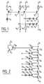
- a main transistor T0 of the pnp type has its emitter connected to a supply voltage source V c through a resistor R0, and its collector connected to the emitter of a transistor T1 whose collector is itself - even connected to the emitter of a transistor T2.
- the base of the transistors T1 and T2 is connected to two diodes in series and in the direct direction (D1, D'1) and (D2, D'2) and whose function is to force the operation of the transistors T1 and T2 in BV CEO for low output voltage levels V s .
- patent US 3,940,683 discloses a circuit of different design, and consisting of a current source having cascaded transistors, of which only the main transistor has a direct diode in the base.
- the number of diodes required is dictated by the values of the voltages they must withstand.
- the cathode of the diodes D'2 and D'2 (point A and B respectively) are brought to potentials fixed by current sources (T''1, R''1) and (T''2 , R''2) respectively and the value of resistors R1 and R2 disposed respectively between points A and B and the common mode pole.
- a transistor T3 whose base and collector are short-circuited and cooperating with a current source I3, forms a current mirror in a conventional manner with the transistors T0, T''1 and T''2.
- the output voltage Vs is available at the collector of transistor T2. This output voltage changes according to the load applied to the collector of transistor T2.
- the transistors T1 and T2 work in the BV CEO mode, the transistor T0 remaining in a conventional operating mode.
- the output voltage Vs approaches the value of the supply voltage Vc (for example 30V)
- the transistors T1, T2 and T3 work in saturation.
- the problem with this arrangement is the difficulty of producing integrated pnp transistors providing sufficient collector current for certain applications, for example 1 mA to supply a Varicap diode from a radio or TV receiver tuner.
- this current problem is solved by using cells comprising a pnp transistor and an npn transistor.
- the collector current of the pnp transistor is divided by the current gain ⁇ of the associated npn transistor, which can in turn supply sufficient current.
- each cell consists of an npn transistor (T10 .... T15) and a pnp transistor (T'10 ... T'15) the collector of the pnp transistor being connected to the base of the npn transistor, and the emitter of the pnp transistor, to the collector of the npn transistors.
- This type of cell is known per se, for current sources, from patent GB 1 285 621 (fig. 9) or German patent applications DE-OS 2 157 626 or DE-OS 2 738 205.
- the transistors T'11 to T'13 have live diodes respectively D11, D12, D13, D14 and D'14, D15 and D'15 connected to their base and each referenced to a given fixed potential.
- Transistors T16 and T17 are arranged so as to form with the transistor T10 a current mirror.
- V smax Vc -5.4V
- Figure 3 corresponds to an assembly making it possible to reduce this difference and bring it down to around 6V CEsat npn .
- emitters of transistors T'10 to T'15 are no longer connected to the collectors of transistors T10 to T15, but referenced to fixed potentials through resistors R'10 to R'15.
- the transistor T'15 For low output levels, the transistor T'15 must operate at maximum in BV CEO , and the emitter voltage of the transistor T'15 must be fixed at approximately V s (min) + V BEnpn + BV CEO , V s (min) designating the minimum value of the retention V s .
- the collector voltage of the transistor T'15 must be very close to V C. This implies a reverse operation of this transistor and therefore the limitations of the use of this assembly with regard to the output levels.
- the assembly according to the invention comprises transistors T30 to T35 of the npn type, the collector-emitter paths of which are connected in series like those of the transistors T10 to T15.
- a transistor T'30 whose collector is connected to the base of transistor T30, and whose emitter is connected to the supply voltage source V C is mounted in conventional manner as a current mirror with transistors T36 and T37.
- Transistors T'31 to T'35 constituting control transistors associated respectively with the output transistors T31 to T35 have their collector connected to the base respectively of the transistors T31 to T35.
- the emitter of the transistors T'31 and T'32 is connected to the supply voltage source V C , while that of the transistors T'33 to T'35 is connected to the collector of the transistors respectively T31 to T33.
- the bases of the transistors T'31 to T'35 are connected to direct diodes respectively D31, D32, D33 and D'33, D34 and D'34, D35 and D'35, which have the function of allowing operation in BV CEO at low output voltages Vs at the emitter of transistor T35.
- the basic reference potential of the transistors T'31 to T'35 is determined by current sources constituted by transistors T''31 to T''35 mounted in current mirror with the transistors T36 and T37, and by four resistors arranged in series R32 to R35.
- the resistors R32 to R34 are connected in parallel between the cathodes of the diodes D32 and D'33 respectively.
- the emitting potential for example of the transistor T'35 is the same as that of the collector of the transistor T33 which avoids the drawback of the experimental arrangement of FIG. 3, since the emitter voltage of the transistors T ' 33, T'34 and T'35 changes as a function of the output voltage V s .
- V BE be the base-emitter voltage of a transistor (around 0.7V)
- V n be the collector-emitter voltage of a saturated npn transistor
- V p be the collector-emitter voltage of a saturated pnp transistor.
- the transistors T30 to T35 and T'30 to T'35 are saturated.
- the transmitter voltage of T30 can reach the value V c -V p -V BE
- the transmitter voltage of T31 can reach the value V c -V p -V n -V BE
- the transmitter voltage of T32 can reach the value V c -V p -2V n -V BE
- the transmitter voltage of T33 can reach the value V c -2V p -2V BE
- the transmitter voltage of T34 can reach the value V c -2V p -V n -2V BE .
- the maximum output voltage Vs available at the emitter of transistor T35 can reach the value V c -2V p -2V n -2V BE .
- the diodes being produced from npn transistors, supporting a maximum voltage of 20V (operation in BV CBO ), and the voltages to be supported being greater than this value for the bases of the transistors T'33 to T'35, two diodes are necessary for these transistors.
- a condition to be respected is that the transistors T30 and T'30 do not leave in avalanche because it is the two transistors which limit the current.
- the resistance bridge R32 to R35 is advantageously provided so that the basic potential of the transistors T'33 to T'35 has the maximum value corresponding to the minimum possible value for the collector-emitter voltages of the transistors T30 to T32.
- the collector voltage of transistor T31 for example is equal to V B ′ + 3V BE , V B ′ denoting the voltage at point B '.
- V A ' , V C' and V D ′ be the potentials of points A ', C' and D '.
- V D31 voltage across the diode D31
- V BE (T'31) base-emitter voltage of transistor T'31 in the BV CEO region.
- the diagram in FIG. 4 therefore makes it possible to obtain the advantages obtained by those of FIGS. 2 and 3 without presenting their shortcomings.
- the diagram of Figure 4 has an additional advantage, in that the difference between the currents collector of transistors T30 and T35 is weak, unlike the case of FIG. 3, because the currents consumed by the pnp transistors are reinjected on the npn transistors.
- Another advantage of this arrangement is that it can operate even in the case where the transistors T'33 to T'35 are in the BV CEO mode, since the main current is limited by the transistor T30.
Landscapes
- Engineering & Computer Science (AREA)
- Physics & Mathematics (AREA)
- Electromagnetism (AREA)
- General Physics & Mathematics (AREA)
- Radar, Positioning & Navigation (AREA)
- Automation & Control Theory (AREA)
- Amplifiers (AREA)
- Control Of Electrical Variables (AREA)
- Bipolar Integrated Circuits (AREA)
Claims (4)
- Stromquelle mit breitem Ausgangsspannungsbereich, in der die EmitterKollektor-Strecke eines Haupttransistors, der so beschaffen ist, daß er die Stromstärke der Stromquelle definiert, mit der Emitter-Kollektor-Strecke mindestens eines Ausgangstransistors in Reihe geschaltet ist, dadurch gekennzeichnet, daß sie n Ausgangstransistoren vom npn-Typ (T₃₁ - T₃₅) hat, mit n ≧ 2, wobei der Kollektor des ersten Ausgangstransistors (T₃₁) mit dem Emitter des Haupttransistors (T₃₀), der ebenfalls vom npn-Typ ist, verbunden ist, der Kollektor des p-ten Ausgangstransistors, mit 1< p ≦n, mit dem Emitter des (p-1)-ten Ausgangstransistors verbunden ist, wobei der Emitter des n-ten Ausgangstransistors den Ausgang der Stromquelle bildet, und daß jedem q-ten Ausgangstransistor (T₃₁-T₃₅) ein q-ter Steuertransistor vom entgegengesetzten Typ (T'₃₁,...T'₃₅) zugeordnet ist, dessen Basis mindestens eine auf ein q-tes Bezugspotential bezogene, in Vorwärtsrichtung geschaltete Diode enthalt, dessen Kollektor mit der Basis des q-ten Ausgangstransistors (T₃₁,...T₃₅) verbunden und dessen Emitter fuhr q > r mit dem Kollektor des (q-r)-ten Ausgangstransistors und für q ≦ r mit dem Kollektor des Haupttransistors (T₃₀) sowie mit einer Speisespannungsquelle verbunden ist, mit r > 1.
- Stromquelle nach Anspruch 1, dadurch gekennzeichnet, daß r < E(b)-1, wobei E(b) den ganzzahligen Teil des Verlältnisses zwischen den BVCEO-Werten der npn- und pnp-Transistoren angibt.
- Stromquelle nach Anspruch 2, dadurch gekennzeichnet, daß r = 2 und p = 5.
- Stromquelle einem der Ansprüche 1 bis 3, dadurch gekennzeichnet, daß das genannte Bezugspotential auf den Maximalwert festgelegt ist, der dem minimal möglichen Wert für die Kollektor-Emitter-Spannungen der Ausgangstransistoren im Sättigungsbetrieb entspricht.
Applications Claiming Priority (2)
| Application Number | Priority Date | Filing Date | Title |
|---|---|---|---|
| FR8802772A FR2628230B1 (fr) | 1988-03-04 | 1988-03-04 | Source de courant a gamme etendue de tensions de sortie |
| FR8802772 | 1988-03-04 |
Publications (2)
| Publication Number | Publication Date |
|---|---|
| EP0331253A1 EP0331253A1 (de) | 1989-09-06 |
| EP0331253B1 true EP0331253B1 (de) | 1993-07-28 |
Family
ID=9363918
Family Applications (1)
| Application Number | Title | Priority Date | Filing Date |
|---|---|---|---|
| EP89200468A Expired - Lifetime EP0331253B1 (de) | 1988-03-04 | 1989-02-27 | Stromquelle mit einem breiten Bereich an Ausgangsspannungen |
Country Status (7)
| Country | Link |
|---|---|
| US (1) | US4901002A (de) |
| EP (1) | EP0331253B1 (de) |
| JP (1) | JPH01266613A (de) |
| KR (1) | KR890015505A (de) |
| DE (1) | DE68907748T2 (de) |
| FR (1) | FR2628230B1 (de) |
| HK (1) | HK178395A (de) |
Families Citing this family (2)
| Publication number | Priority date | Publication date | Assignee | Title |
|---|---|---|---|---|
| JP3686176B2 (ja) * | 1996-08-06 | 2005-08-24 | 株式会社ルネサステクノロジ | 定電流発生回路及び内部電源電圧発生回路 |
| DE102006007479B4 (de) * | 2006-02-17 | 2017-08-10 | Infineon Technologies Ag | Shunt-Regler |
Family Cites Families (7)
| Publication number | Priority date | Publication date | Assignee | Title |
|---|---|---|---|---|
| US2888525A (en) * | 1956-03-02 | 1959-05-26 | Emerson Electric Mfg Co | Telescopic voltage amplifier |
| DE1226193B (de) * | 1959-03-26 | 1966-10-06 | Siemens Ag | Schaltungsanordnung zur Regelung der Ausgangsspannung eines Mittelspannungs-netzgeraetes mittels Transistoren |
| GB937506A (en) * | 1960-12-01 | 1963-09-25 | Westinghouse Brake & Signal | Improvements relating to power transistors and voltage regulating circuits therefor |
| US3181010A (en) * | 1962-12-28 | 1965-04-27 | North American Aviation Inc | Transistor current control circuit |
| DE2256603C3 (de) * | 1972-11-17 | 1978-04-20 | Siemens Ag, 1000 Berlin Und 8000 Muenchen | Transistor-Regelschaltung zur Gewinnung einer konstanten Gleichspannung |
| US3940683A (en) * | 1974-08-12 | 1976-02-24 | Signetics Corporation | Active breakdown circuit for increasing the operating range of circuit elements |
| US4166971A (en) * | 1978-03-23 | 1979-09-04 | Bell Telephone Laboratories, Incorporated | Current mirror arrays |
-
1988
- 1988-03-04 FR FR8802772A patent/FR2628230B1/fr not_active Expired - Fee Related
-
1989
- 1989-02-23 US US07/315,009 patent/US4901002A/en not_active Expired - Fee Related
- 1989-02-27 DE DE89200468T patent/DE68907748T2/de not_active Expired - Fee Related
- 1989-02-27 EP EP89200468A patent/EP0331253B1/de not_active Expired - Lifetime
- 1989-03-02 KR KR1019890002549A patent/KR890015505A/ko not_active Abandoned
- 1989-03-04 JP JP1051016A patent/JPH01266613A/ja active Pending
-
1995
- 1995-11-23 HK HK178395A patent/HK178395A/xx not_active IP Right Cessation
Also Published As
| Publication number | Publication date |
|---|---|
| KR890015505A (ko) | 1989-10-30 |
| US4901002A (en) | 1990-02-13 |
| JPH01266613A (ja) | 1989-10-24 |
| FR2628230B1 (fr) | 1990-06-22 |
| DE68907748T2 (de) | 1994-02-10 |
| FR2628230A1 (fr) | 1989-09-08 |
| HK178395A (en) | 1995-12-01 |
| EP0331253A1 (de) | 1989-09-06 |
| DE68907748D1 (de) | 1993-09-02 |
Similar Documents
| Publication | Publication Date | Title |
|---|---|---|
| EP0838745B1 (de) | Spannungsregler mit automatischer Auswahl der höchsten Versorgungsspannung | |
| EP0388329B1 (de) | Steuerschaltung für einen MOS-Leistungstransistor mit induktiver Last | |
| US3560750A (en) | Optoelectronic amplifier | |
| EP0029767B1 (de) | Steuerungsverfahren einer Darlingtonschaltung und Darlingtonschaltung mit geringen Verlusten | |
| EP0153774B1 (de) | ECL-kompatible elementare logische Schaltung aus Gallium-Arsenid-Transistoren hergestellt | |
| EP0082071A1 (de) | Einrichtung für die Umschaltung einer mit mindestens einem gesteuerten Schalter versehenen Gleichspannungsquelle und Kommutierungshilfsschaltung für eine solche Einrichtung | |
| EP0432058A1 (de) | Dynamische Isolierschaltung für integrierte Schaltungen | |
| EP1695332A2 (de) | Elektronische steuerzelle für eine organische elektrolumineszenzdiode einer aktivmatrixanzeige und verfahren zu ihrem betrieb und anzeige | |
| EP0159233B1 (de) | Steuerschaltung zum Schalten eines Leistungstransistors | |
| EP0649079B1 (de) | Geregelter Spannungsquellengenerator der Bandgapbauart | |
| EP0201136A1 (de) | Digitales Multiplexermodul mit N-Eingängen und solche Module enthaltender Multiplexer mit N-Quadrat-Eingängen | |
| EP0248473B1 (de) | Umsetzerschaltung mit drei logischen Zuständen | |
| EP0237094A1 (de) | Vordiffundierte Gatterfeld-Halbleitervorrichtung für speziell hergestellte Schaltungen | |
| EP0359680A1 (de) | Integrierbare, aktive Diode | |
| EP0331253A1 (de) | Stromquelle mit einem breiten Bereich an Ausgangsspannungen | |
| US20030091076A1 (en) | Optical source driver with improved input stage | |
| EP0048782A1 (de) | Decodier- und Auswahlschaltung für einen monolithischen Speicher | |
| EP0200255B1 (de) | Schaltstufe einer Darlington-Type insbesondere für Speicher-Wortzeile-Dekodierer | |
| EP0816965B1 (de) | Temperaturabhängig geregelter Referenzspannungsgenerator | |
| CA1074862A (fr) | Generateur de tres haute tension commutable | |
| FR2542946A1 (fr) | Amplificateur differentiel a transistors bipolaires realises en technologie cmos | |
| EP0384863B1 (de) | TTL-kompatible Ausgangsschaltung mit hoher Schaltgeschwindigkeit | |
| EP0230176B1 (de) | Statisches Relais, sowie Anwendung dieses Relais bei einem bipolaren Inverter oder bei einer Schaltung mit beliebiger Stromrichtung | |
| EP0102675A2 (de) | Transistor-Transistor logische Schaltung mit Hysteresis | |
| FR2648643A1 (fr) | Circuit d'interface entre deux circuits numeriques de natures differentes |
Legal Events
| Date | Code | Title | Description |
|---|---|---|---|
| PUAI | Public reference made under article 153(3) epc to a published international application that has entered the european phase |
Free format text: ORIGINAL CODE: 0009012 |
|
| AK | Designated contracting states |
Kind code of ref document: A1 Designated state(s): DE FR GB IT NL |
|
| 17P | Request for examination filed |
Effective date: 19900301 |
|
| RAP1 | Party data changed (applicant data changed or rights of an application transferred) |
Owner name: N.V. PHILIPS' GLOEILAMPENFABRIEKEN Owner name: PHILIPS COMPOSANTS |
|
| 17Q | First examination report despatched |
Effective date: 19921005 |
|
| GRAA | (expected) grant |
Free format text: ORIGINAL CODE: 0009210 |
|
| RAP1 | Party data changed (applicant data changed or rights of an application transferred) |
Owner name: N.V. PHILIPS' GLOEILAMPENFABRIEKEN Owner name: PHILIPS COMPOSANTS |
|
| AK | Designated contracting states |
Kind code of ref document: B1 Designated state(s): DE FR GB IT NL |
|
| PG25 | Lapsed in a contracting state [announced via postgrant information from national office to epo] |
Ref country code: NL Effective date: 19930728 |
|
| REF | Corresponds to: |
Ref document number: 68907748 Country of ref document: DE Date of ref document: 19930902 |
|
| ITF | It: translation for a ep patent filed | ||
| GBT | Gb: translation of ep patent filed (gb section 77(6)(a)/1977) |
Effective date: 19931018 |
|
| NLV1 | Nl: lapsed or annulled due to failure to fulfill the requirements of art. 29p and 29m of the patents act | ||
| ITTA | It: last paid annual fee | ||
| PLBE | No opposition filed within time limit |
Free format text: ORIGINAL CODE: 0009261 |
|
| STAA | Information on the status of an ep patent application or granted ep patent |
Free format text: STATUS: NO OPPOSITION FILED WITHIN TIME LIMIT |
|
| 26N | No opposition filed | ||
| ITPR | It: changes in ownership of a european patent |
Owner name: CAMBIO RAGIONE SOCIALE;PHILIPS ELECTRONICS N.V. |
|
| PGFP | Annual fee paid to national office [announced via postgrant information from national office to epo] |
Ref country code: DE Payment date: 19950424 Year of fee payment: 7 |
|
| PGFP | Annual fee paid to national office [announced via postgrant information from national office to epo] |
Ref country code: GB Payment date: 19960131 Year of fee payment: 8 |
|
| PGFP | Annual fee paid to national office [announced via postgrant information from national office to epo] |
Ref country code: FR Payment date: 19960228 Year of fee payment: 8 |
|
| REG | Reference to a national code |
Ref country code: FR Ref legal event code: CD |
|
| PG25 | Lapsed in a contracting state [announced via postgrant information from national office to epo] |
Ref country code: DE Effective date: 19961101 |
|
| PG25 | Lapsed in a contracting state [announced via postgrant information from national office to epo] |
Ref country code: GB Effective date: 19970227 |
|
| GBPC | Gb: european patent ceased through non-payment of renewal fee |
Effective date: 19970227 |
|
| PG25 | Lapsed in a contracting state [announced via postgrant information from national office to epo] |
Ref country code: FR Effective date: 19971030 |
|
| REG | Reference to a national code |
Ref country code: FR Ref legal event code: ST |
|
| PG25 | Lapsed in a contracting state [announced via postgrant information from national office to epo] |
Ref country code: IT Free format text: LAPSE BECAUSE OF NON-PAYMENT OF DUE FEES;WARNING: LAPSES OF ITALIAN PATENTS WITH EFFECTIVE DATE BEFORE 2007 MAY HAVE OCCURRED AT ANY TIME BEFORE 2007. THE CORRECT EFFECTIVE DATE MAY BE DIFFERENT FROM THE ONE RECORDED. Effective date: 20050227 |