US4901002A - Current source having a wide range of output voltages - Google Patents
Current source having a wide range of output voltages Download PDFInfo
- Publication number
- US4901002A US4901002A US07/315,009 US31500989A US4901002A US 4901002 A US4901002 A US 4901002A US 31500989 A US31500989 A US 31500989A US 4901002 A US4901002 A US 4901002A
- Authority
- US
- United States
- Prior art keywords
- transistor
- collector
- emitter
- output
- transistors
- Prior art date
- Legal status (The legal status is an assumption and is not a legal conclusion. Google has not performed a legal analysis and makes no representation as to the accuracy of the status listed.)
- Expired - Fee Related
Links
- 229920006395 saturated elastomer Polymers 0.000 description 4
- 238000004519 manufacturing process Methods 0.000 description 2
- 230000008878 coupling Effects 0.000 description 1
- 238000010168 coupling process Methods 0.000 description 1
- 238000005859 coupling reaction Methods 0.000 description 1
- 238000000034 method Methods 0.000 description 1
Images
Classifications
-
- G—PHYSICS
- G05—CONTROLLING; REGULATING
- G05F—SYSTEMS FOR REGULATING ELECTRIC OR MAGNETIC VARIABLES
- G05F1/00—Automatic systems in which deviations of an electric quantity from one or more predetermined values are detected at the output of the system and fed back to a device within the system to restore the detected quantity to its predetermined value or values, i.e. retroactive systems
- G05F1/10—Regulating voltage or current
- G05F1/46—Regulating voltage or current wherein the variable actually regulated by the final control device is DC
- G05F1/56—Regulating voltage or current wherein the variable actually regulated by the final control device is DC using semiconductor devices in series with the load as final control devices
- G05F1/565—Regulating voltage or current wherein the variable actually regulated by the final control device is DC using semiconductor devices in series with the load as final control devices sensing a condition of the system or its load in addition to means responsive to deviations in the output of the system, e.g. current, voltage, power factor
-
- G—PHYSICS
- G05—CONTROLLING; REGULATING
- G05F—SYSTEMS FOR REGULATING ELECTRIC OR MAGNETIC VARIABLES
- G05F1/00—Automatic systems in which deviations of an electric quantity from one or more predetermined values are detected at the output of the system and fed back to a device within the system to restore the detected quantity to its predetermined value or values, i.e. retroactive systems
- G05F1/10—Regulating voltage or current
- G05F1/46—Regulating voltage or current wherein the variable actually regulated by the final control device is DC
- G05F1/56—Regulating voltage or current wherein the variable actually regulated by the final control device is DC using semiconductor devices in series with the load as final control devices
- G05F1/59—Regulating voltage or current wherein the variable actually regulated by the final control device is DC using semiconductor devices in series with the load as final control devices including plural semiconductor devices as final control devices for a single load
- G05F1/595—Regulating voltage or current wherein the variable actually regulated by the final control device is DC using semiconductor devices in series with the load as final control devices including plural semiconductor devices as final control devices for a single load semiconductor devices connected in series
Definitions
- the present invention relates to a current source having a wide range of output voltages, in which source the emitter-collector path of a main transistor, arranged to define the value of the current of the current source, is arranged in series with the emitter-collector path of at least one output transistor.
- the invention proposes a current source of the type defined in the opening paragraph, whose current is comparatively large and which can operate at output voltages ranging between one collector-emitter voltage of an output transistor in the saturation mode V CEsat and a value as close as possible to the supply voltage.
- the principle underlying the invention is to combine each output transistor with an associated control transistor of the opposite type whose emitter potential is fixed by coupling this control transistor to another stage, and to operate the output transistors in the BV CEO mode for low output voltages.
- the current source in accordance with the invention is therefore characterized in that it comprises n output transistors, where n ⁇ 2, the first output transistor having its collector connected to the emitter of the main transistor, the p th transistor, where 1 ⁇ p ⁇ n, having its collector connected to the emitter of the (p-1) th transistor, the emitter of the n th transistor constituting the output of the current source, and in that every q th output transistor is associated with a q th control transistor of the opposite type, whose base includes at least one diode poled in the forward direction and referred (i.e.
- U.S. Pat. No. 3,940,683 discloses a circuit of different design, consisting of a current source comprising cascaded transistors in which only the main transistor includes a diode poled in the forward direction in its base.
- said reference potentials are each fixed at the maximum value corresponding to the minimum possible values for the collector-emitter voltages of the output transistors in the saturation mode V CEsat .
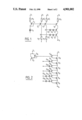
- FIGS. 1 to 3 by way of illustration show test circuits not previously published by the Applicant.
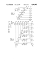
- FIG. 4 shows an embodiment of the invention.
- a pnp-type main transistor T 0 has its emitter coupled to a supply voltage source V c via a resistor R 0 and has its collector connected to the emitter of a transistor T 1 whose collector is connected to the emitter of a transistor T 2 .
- the transistors T 1 and T 2 have their bases connected to two diodes in series, which diodes (D 1 , D' 1 ) and (D 2 , D' 2 ) are poled in the forward direction and serve to ensure that the transistors T 1 and T 2 are operated in the BV CEO mode for low levels of the output voltage V s .
- the number of diodes needed is dictated by the values of the voltages to be handled by these diodes.
- the cathodes of the diodes D' 1 and D' 2 are brought to potentials determined by the current sources (T" 1 , R" 1 ) and (T" 2 , R" 2 ) respectively and by the values of the resistors R 1 and R 2 , which are respectively arranged between points A and B and the common mode terminal.
- a transistor T 3 having its base and collector short-circuited and cooperating with a current source I 3 constitutes a conventional current mirror with the transistors T 0 , T" 1 and T" 2 .
- the output voltage V s is available on the collector of the transistor T 2 . This output voltage varies depending on the load applied to the collector of the transistor T 2 .
- the transistors T 1 and T 2 When the output voltage V s is low (for example of the order of 0.7 V) the transistors T 1 and T 2 will operate in the BV CEO mode, while the transistor T 0 remains in a normal mode of operation. When the output voltage V s approximates to the value of the supply voltage V c (for example, 30 V) the transistors T 1 , T 2 and T 0 will operate in the saturation mode.
- this current problem is solved by employing cells comprising a pnp transistor and an npn transistor.
- the collector current of the pnp transistor is divided by the current gain ⁇ of the associated npn transistor, which itself can supply an adequate current.
- each cell comprises an npn transistor (T 10 . . . T 15 ) and a pnp transistor (T' 10 . . . T' 15 ), the collector of the pnp transistor being connected to the base of the associated npn transistor and the emitter of the pnp transistor being connected to the collector of the npn transistor.
- This type of cell for use in current sources, is known per se, from GB 1,285,621 (FIG. 9) or German patent application DE-OS 2,157,626 or DE-OS 2,738,205.
- the transistors T' 11 to T' 15 have diodes D 11 , D 12 , D 13 , D 14 and D' 14 , D 15 and D' 15 respectively, poled in the forward direction, connected to their bases and each referred to a given fixed potential.
- the transistors T 16 and T 17 are arranged to form a current mirror with the transistor T 10 .
- npn transistors have been replaced by six cells because the BV CEO of an npn transistor is smaller than that of a pnp transistor, in the present example by a factor of approximately 3.
- V s i.e. the output voltage available on the emitter of T 15 .
- V BE npn base-emitter voltage of an npn transistor ⁇ 0.8 V
- FIG. 3 relates to a circuit arrangement which enables this difference to be reduced and to be brought to approximately 6 V CEsat npn.
- the emitter of the transistors T' 11 to T' 15 are no longer connected to the collectors of the transistors T 11 to T 15 , but are coupled to fixed reference potentials via resistors R' 11 to R' 15 .
- the transistor T' 15 For low output levels the transistor T' 15 should be operated fully in the BV CEO mode and the emitter voltage of the transistor T' 15 should be fixed at approximately V s (min) +V BEnpn +BV CEO , V s (min) being the minimum value of the voltage V s .
- the circuit arrangement in accordance with the invention shown in FIG. 4 comprises npn type transistors T 30 to T 35 whose collector-emitter paths are arranged in series in the same way as those of the transistors T 10 to T 15 .
- a transistor T' 30 having its collector connected to the base of the transistor T 30 and having its emitter connected to the supply voltage source V c is arranged as a conventional current mirror with the transistors T 36 and T 37 .
- the transistors T' 31 to T' 35 constituting the control transistors associated with the output transistors T 31 to T 35 have their collectors connected to the bases of the transistors T 31 to T 35 respectively.
- the emitters of the transistors T' 31 and T' 32 are connected to the supply voltage source V C
- the emitters of the transistors T' 33 to T' 35 are connected to the collectors of the transistors T 31 to T 33 respectively.
- the bases of the transistors T' 31 to T' 35 are connected to diodes D 31 , D 32 , D 33 and D' 33 , D 34 and D' 34 , D 35 and D' 35 respectively, which diodes are poled in the forward direction and serve to enable operation in the BV CEO mode in the case of low output voltages V s on the emitter of the transistor T 35 .
- the base reference potential of the transistors T' 31 to T' 35 is determined by current sources formed by the transistors T" 31 to T" 35 arranged as a current mirror with the transistors T 36 and T 37 , and by four resistors R 32 to R 35 arranged in series.
- the resistors R 32 to R 34 are arranged in parallel between the cathodes of the diodes D 32 and D' 33 (points A' and B'), D' 33 and D' 34 (points B' and C'), D' 34 and D' 35 (points C' and D') respectively.
- the resistor R 35 is arranged between the cathode of the diode D' 35 and the common-mode terminal.
- b-1 2 places in rank.
- E(b)-1 the maximum of (aliquot part of b)-1, i.e E(b)-1.
- the integer part E(b) of a number "b" is the portion of the number to the left of the decimal point.
- the emitter potential of, for example, the transistor T' 35 is equal to the collector potential of the transistor T 33 , so that the drawback of the experimental circuit shown in FIG. 3 is avoided, because the emitter voltage of the transistors T' 33 , T' 34 and T' 35 varies as a functionion of the output voltage V s .
- the maximum voltage available on the output is closer to V c than in the experimental circuit of FIG. 2.
- V BE be the base-emitter voltage of a transistor (approximately 0.7 V).
- V n be the emitter-collector voltage of a saturated npn transistor.
- V p be the emitter-collector voltage of a saturated pnp transistor.
- the emitter voltage of T 30 can reach the value
- the emitter voltage of T 31 can reach the value
- the emitter voltage of T 32 can reach the value
- the emitter voltage of T 33 can reach the value
- the emitter voltage of T 34 can reach the value
- the maximum output voltage V s available on the emitter of the transistor T 35 can reach the value
- the circuit can be powered with 30 V, which for example enables a varicap diode to be operated between approximately 0.7 V and 28 V. Since the diodes are formed by means of npn transistors, which can handle a maximum voltage of 20 V (operation in the BV CEO mode), the voltages to be handled being higher than said value for the bases of the transistors T' 33 to T' 35 , two diodes are required for these transistors.
- a requirement to be met is that the transistors T 30 and T' 30 should not come into the avalanche region because these are the two transistors which limit the current.
- the collector voltage of the transistor T 31 is, for example, V B' +3V BE , V B' being the voltage on point B'.
- the potentials on points A', C' and D' are referred to as V A' , V C' and V D' .
- V D31 is the voltage across the diode D 31
- V BE (T' 31 ) the base-emitter voltage of the transistor T' 31 in the BV CEO region.
- the circuit shown in FIG. 4 enables the advantages of the circuits shown in FIGS. 2 and 3 to be obtained without their drawbacks.
- the circuits shown in FIG. 4 has the additional advantage that the difference between the collector currents of the transistors T 30 and T 35 is small in comparison with the situation in FIG. 3, because the currents drawn by the pnp transistors are re-injected into the npn transistors.
- Another advantage of this circuit arrangement is that it can operate even in the case where the transistors T' 33 to T' 35 are in the BV CEO mode, the main current being limited by the transistor T 30 .
Landscapes
- Engineering & Computer Science (AREA)
- Physics & Mathematics (AREA)
- Electromagnetism (AREA)
- General Physics & Mathematics (AREA)
- Radar, Positioning & Navigation (AREA)
- Automation & Control Theory (AREA)
- Amplifiers (AREA)
- Control Of Electrical Variables (AREA)
- Bipolar Integrated Circuits (AREA)
Applications Claiming Priority (2)
| Application Number | Priority Date | Filing Date | Title |
|---|---|---|---|
| FR8802772A FR2628230B1 (fr) | 1988-03-04 | 1988-03-04 | Source de courant a gamme etendue de tensions de sortie |
| FR8802772 | 1988-03-04 |
Publications (1)
| Publication Number | Publication Date |
|---|---|
| US4901002A true US4901002A (en) | 1990-02-13 |
Family
ID=9363918
Family Applications (1)
| Application Number | Title | Priority Date | Filing Date |
|---|---|---|---|
| US07/315,009 Expired - Fee Related US4901002A (en) | 1988-03-04 | 1989-02-23 | Current source having a wide range of output voltages |
Country Status (7)
| Country | Link |
|---|---|
| US (1) | US4901002A (de) |
| EP (1) | EP0331253B1 (de) |
| JP (1) | JPH01266613A (de) |
| KR (1) | KR890015505A (de) |
| DE (1) | DE68907748T2 (de) |
| FR (1) | FR2628230B1 (de) |
| HK (1) | HK178395A (de) |
Cited By (2)
| Publication number | Priority date | Publication date | Assignee | Title |
|---|---|---|---|---|
| US5757175A (en) * | 1996-08-06 | 1998-05-26 | Mitsubishi Denki Kabushiki Kaisha | Constant current generating circuit |
| US8085006B2 (en) | 2006-02-17 | 2011-12-27 | Infineon Technologies Ag | Shunt regulator |
Citations (3)
| Publication number | Priority date | Publication date | Assignee | Title |
|---|---|---|---|---|
| US2888525A (en) * | 1956-03-02 | 1959-05-26 | Emerson Electric Mfg Co | Telescopic voltage amplifier |
| US3940683A (en) * | 1974-08-12 | 1976-02-24 | Signetics Corporation | Active breakdown circuit for increasing the operating range of circuit elements |
| US4166971A (en) * | 1978-03-23 | 1979-09-04 | Bell Telephone Laboratories, Incorporated | Current mirror arrays |
Family Cites Families (4)
| Publication number | Priority date | Publication date | Assignee | Title |
|---|---|---|---|---|
| DE1226193B (de) * | 1959-03-26 | 1966-10-06 | Siemens Ag | Schaltungsanordnung zur Regelung der Ausgangsspannung eines Mittelspannungs-netzgeraetes mittels Transistoren |
| GB937506A (en) * | 1960-12-01 | 1963-09-25 | Westinghouse Brake & Signal | Improvements relating to power transistors and voltage regulating circuits therefor |
| US3181010A (en) * | 1962-12-28 | 1965-04-27 | North American Aviation Inc | Transistor current control circuit |
| DE2256603C3 (de) * | 1972-11-17 | 1978-04-20 | Siemens Ag, 1000 Berlin Und 8000 Muenchen | Transistor-Regelschaltung zur Gewinnung einer konstanten Gleichspannung |
-
1988
- 1988-03-04 FR FR8802772A patent/FR2628230B1/fr not_active Expired - Fee Related
-
1989
- 1989-02-23 US US07/315,009 patent/US4901002A/en not_active Expired - Fee Related
- 1989-02-27 DE DE89200468T patent/DE68907748T2/de not_active Expired - Fee Related
- 1989-02-27 EP EP89200468A patent/EP0331253B1/de not_active Expired - Lifetime
- 1989-03-02 KR KR1019890002549A patent/KR890015505A/ko not_active Abandoned
- 1989-03-04 JP JP1051016A patent/JPH01266613A/ja active Pending
-
1995
- 1995-11-23 HK HK178395A patent/HK178395A/xx not_active IP Right Cessation
Patent Citations (3)
| Publication number | Priority date | Publication date | Assignee | Title |
|---|---|---|---|---|
| US2888525A (en) * | 1956-03-02 | 1959-05-26 | Emerson Electric Mfg Co | Telescopic voltage amplifier |
| US3940683A (en) * | 1974-08-12 | 1976-02-24 | Signetics Corporation | Active breakdown circuit for increasing the operating range of circuit elements |
| US4166971A (en) * | 1978-03-23 | 1979-09-04 | Bell Telephone Laboratories, Incorporated | Current mirror arrays |
Cited By (2)
| Publication number | Priority date | Publication date | Assignee | Title |
|---|---|---|---|---|
| US5757175A (en) * | 1996-08-06 | 1998-05-26 | Mitsubishi Denki Kabushiki Kaisha | Constant current generating circuit |
| US8085006B2 (en) | 2006-02-17 | 2011-12-27 | Infineon Technologies Ag | Shunt regulator |
Also Published As
| Publication number | Publication date |
|---|---|
| KR890015505A (ko) | 1989-10-30 |
| JPH01266613A (ja) | 1989-10-24 |
| FR2628230B1 (fr) | 1990-06-22 |
| DE68907748T2 (de) | 1994-02-10 |
| FR2628230A1 (fr) | 1989-09-08 |
| EP0331253B1 (de) | 1993-07-28 |
| HK178395A (en) | 1995-12-01 |
| EP0331253A1 (de) | 1989-09-06 |
| DE68907748D1 (de) | 1993-09-02 |
Similar Documents
| Publication | Publication Date | Title |
|---|---|---|
| US4806790A (en) | Sample-and-hold circuit | |
| US3743850A (en) | Integrated current supply circuit | |
| US4109162A (en) | Multi-stage integrated injection logic circuit with current mirror | |
| US4329597A (en) | Logic circuit | |
| US4864166A (en) | Tri-state logic level converter circuit | |
| GB1598899A (en) | Logic circuits | |
| US5359241A (en) | ECL circuit | |
| US4658205A (en) | Reference voltage generating circuit | |
| US4833344A (en) | Low voltage bias circuit | |
| US4429270A (en) | Switched current source for sourcing current to and sinking current from an output node | |
| US3828241A (en) | Regulated voltage supply circuit which compensates for temperature and input voltage variations | |
| US4221979A (en) | Non-inverting buffer circuits | |
| US4977336A (en) | Schmitt-trigger circuit having no discrete resistor | |
| US5099139A (en) | Voltage-current converting circuit having an output switching function | |
| JPS6038925A (ja) | 信号変換器 | |
| EP0102675A2 (de) | Transistor-Transistor logische Schaltung mit Hysteresis | |
| US4590389A (en) | Compensation circuit and method for stabilization of a circuit node by multiplication of displacement current | |
| US5670868A (en) | Low-constant voltage supply circuit | |
| US4553107A (en) | Current mirror circuit having stabilized output current | |
| US4417292A (en) | Power amplifier protection circuit | |
| EP0161015A1 (de) | Eingangsschaltung zur Lieferung eines die Wirkungsweise steigernden Entladungspfades | |
| US4259599A (en) | Complementary transistor switching circuit | |
| US4171492A (en) | Temperature compensated zener diode arrangement | |
| GB2048597A (en) | Push-pull output circuit | |
| US4501979A (en) | Current amplifier having multiple selectable outputs |
Legal Events
| Date | Code | Title | Description |
|---|---|---|---|
| AS | Assignment |
Owner name: U.S. PHILIPS CORPORATION, NEW YORK Free format text: ASSIGNMENT OF ASSIGNORS INTEREST.;ASSIGNOR:SIMON, MARC;REEL/FRAME:005092/0530 Effective date: 19890328 |
|
| FEPP | Fee payment procedure |
Free format text: PAYOR NUMBER ASSIGNED (ORIGINAL EVENT CODE: ASPN); ENTITY STATUS OF PATENT OWNER: LARGE ENTITY |
|
| FPAY | Fee payment |
Year of fee payment: 4 |
|
| REMI | Maintenance fee reminder mailed | ||
| LAPS | Lapse for failure to pay maintenance fees | ||
| FP | Lapsed due to failure to pay maintenance fee |
Effective date: 19980218 |
|
| STCH | Information on status: patent discontinuation |
Free format text: PATENT EXPIRED DUE TO NONPAYMENT OF MAINTENANCE FEES UNDER 37 CFR 1.362 |