EP4235500B1 - Ic-kartenregler - Google Patents
Ic-kartenregler Download PDFInfo
- Publication number
- EP4235500B1 EP4235500B1 EP22158957.5A EP22158957A EP4235500B1 EP 4235500 B1 EP4235500 B1 EP 4235500B1 EP 22158957 A EP22158957 A EP 22158957A EP 4235500 B1 EP4235500 B1 EP 4235500B1
- Authority
- EP
- European Patent Office
- Prior art keywords
- voltage
- vcc
- regulator
- card
- output
- Prior art date
- Legal status (The legal status is an assumption and is not a legal conclusion. Google has not performed a legal analysis and makes no representation as to the accuracy of the status listed.)
- Active
Links
Images

Classifications
-
- G—PHYSICS
- G06—COMPUTING OR CALCULATING; COUNTING
- G06K—GRAPHICAL DATA READING; PRESENTATION OF DATA; RECORD CARRIERS; HANDLING RECORD CARRIERS
- G06K19/00—Record carriers for use with machines and with at least a part designed to carry digital markings
- G06K19/06—Record carriers for use with machines and with at least a part designed to carry digital markings characterised by the kind of the digital marking, e.g. shape, nature, code
- G06K19/067—Record carriers with conductive marks, printed circuits or semiconductor circuit elements, e.g. credit or identity cards also with resonating or responding marks without active components
- G06K19/07—Record carriers with conductive marks, printed circuits or semiconductor circuit elements, e.g. credit or identity cards also with resonating or responding marks without active components with integrated circuit chips
- G06K19/0701—Record carriers with conductive marks, printed circuits or semiconductor circuit elements, e.g. credit or identity cards also with resonating or responding marks without active components with integrated circuit chips at least one of the integrated circuit chips comprising an arrangement for power management
-
- G—PHYSICS
- G05—CONTROLLING; REGULATING
- G05F—SYSTEMS FOR REGULATING ELECTRIC OR MAGNETIC VARIABLES
- G05F1/00—Automatic systems in which deviations of an electric quantity from one or more predetermined values are detected at the output of the system and fed back to a device within the system to restore the detected quantity to its predetermined value or values, i.e. retroactive systems
- G05F1/10—Regulating voltage or current
- G05F1/46—Regulating voltage or current wherein the variable actually regulated by the final control device is DC
- G05F1/56—Regulating voltage or current wherein the variable actually regulated by the final control device is DC using semiconductor devices in series with the load as final control devices
- G05F1/575—Regulating voltage or current wherein the variable actually regulated by the final control device is DC using semiconductor devices in series with the load as final control devices characterised by the feedback circuit
Definitions
- the present disclosure relates generally to electronic circuits and more particularly to integrated circuit cards.
- Integrated circuit cards also known as smart cards or IC cards
- IC cards are well known. It becomes increasingly frequent that IC cards operate both in contact and contactless mode. Recent developments of IC cards aim at equipping the cards with peripheral systems such as fingerprint sensors, dynamic readable verifying codes, display, etc.
- Document DE 10 2013 106 078 discloses a circuit and method for selecting a current powering.
- One embodiment addresses all or some of the drawbacks of known IC cards.
- a voltage divider of the regulated voltage provides the third voltage.
- the regulator further comprises a circuit having two inputs respectively coupled, preferably connected to said first and second input terminals and one output providing the fourth voltage.
- said circuit comprises a comparator of the first voltage and the second voltage, which controls switches selectively coupling the first input terminal and the second input terminal to said output providing the fourth voltage.
- said second voltage is a voltage extracted from an electromagnetic field.
- An embodiment provides an integrated circuit card comprising a regulator.
- the card comprises:
- the card further comprises a first integrated circuit and an electronic system external to the integrated circuit, said regulated voltage being intended to supply said external system.
- Figure 1 schematically represents an embodiment of an integrated circuit card.
- An integrated circuit card 1, or IC card, or smart card, to which apply the disclosed embodiments comprises:
- the IC chip 11 contains electronic circuits adapted to the application of the card 1.
- chip 11 comprises a microcontroller adapted to operate and control the other elements of card 1 depending on the application.
- a card 1, as illustrated in figure 1 is usually designated a dual interface smart card.
- the card has two interfaces: One contact interface to communicate with a contact reader and one contactless interface to communicate with a wireless reader (NFC or the like).
- NFC wireless reader
- its electronic circuits are powered via the contact interface or via the wireless interface (via the field generated by the contactless reader).
- chip 11 usually comprises voltage regulators capable of providing supply voltages to the rest of the chip 11.
- An example of application is a banking card with fingerprint sensor.
- Another example of application is a banking card with a display of a changing card verification value (cvv).
- Still another example of application is a card (not necessarily a banking card) with a sensor such as a fingerprint sensor, a temperature sensor, an image sensor, etc.
- a sensor such as a fingerprint sensor, a temperature sensor, an image sensor, etc.
- Still another example of application is a card with a display, for example a counter value display or an image display, etc.
- the external circuit 17 is a sensor such a fingerprint sensor, a temperature sensor, a cvv display, counter value display, an image display, etc.
- the value of the power voltage used by the external embedded system or circuit 17 depends on the application.
- Figure 2 illustrates, schematically and partially, an embodiment of a power supply architecture of a dual interface integrated circuit card.
- the dual interface circuit card 1 comprises a voltage regulator 2 (REG) for regulating a voltage VCC provided by a contact reader (not shown) or a voltage VCC_CL extracted from the field generated by a contactless reader (not shown).
- REG voltage regulator 2
- an oscillating circuit of card 1 comprising the antenna 15 and a parallel capacitor 16 (integrated or not in circuit 11), extracts a signal from the field generated by the reader.
- Terminals 23 and 24 of the oscillating circuit are coupled, preferably connected, to a rectifier 25, which extracts a dc voltage VCC_CL from the signal present at terminals 23 and 24 of the oscillating circuit.
- Two inputs of the regulator circuit 2 are respectively coupled, preferably connected, to rectified outputs 26 and 27 of the rectifier 25. In practice, these outputs are also connected by a capacitor Cin.
- the integrated circuit 11 When operating in contactless mode, the integrated circuit 11 communicates with the contactless reader via antenna 15. For this purpose, communication circuits (no shown) of circuit 11 are coupled to the terminals 23 and 24 of the oscillating circuit.
- An output 28 of regulator circuit 2 provides a regulated voltage VCC_OUT to the external system 17 of card 1.
- the regulated voltage VCC_OUT is, arbitrarily, positive with respect to ground 29 provided either by terminal 22 in contact mode of by terminal 27 in contactless mode.
- the value of the regulated voltage VCC_OUT depends on a value of a reference voltage VREF provided to the regulator 2 by another element (for example a bandgap) of the integrated circuit 11 (not shown).
- the value of the regulated voltage VCC_OUT depends on the application and more particularly to the type of external circuit 17.
- the value of the output regulated voltage VCC_OUT can range from 1.4 volts to 2.5 volts and can take more than 10 different values in this range depending on the application.
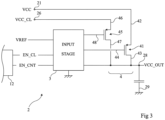
- Figure 3 illustrates, schematically and partially, an embodiment of a voltage regulator of an integrated circuit card.
- the regulator 2 is a linear regulator or Low Drop-Out (LDO) regulator. Power transistors of the regulator 2 couple the respective input terminals of the voltages to be regulated to the output terminal providing the regulated voltage.
- LDO Low Drop-Out
- the regulator 2 comprises:
- transistors 41 and 45 are MOS transistors (preferably PMOS transistors). Respective sources 42 and 46 of transistors 41 and 45 are coupled, preferably connected, to terminals 21 and 26. Respective drains 43 and 47 of transistors 41 and 45 are coupled, preferably connected, to output terminal 28. Respective gates 44 and 48 of transistors 41 and 45 are coupled, preferably connected, to the input stage 3 of the regulator 2.
- both power transistors 41 and 45 of regulator 2 share a common input stage 3.
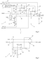
- Figure 4 schematically details an embodiment of the regulator 2 of figure 3 .
- the input stage 3 of the regulator 2 comprises an error amplifier 31, or gain stage, of the difference between a feedback voltage VFB, proportional to the regulated output voltage VCC_OUT, and the reference voltage VREF.
- the amplifier 31 provides, at an output 312, an analog signal, function of this difference between voltages VCC_OUT and VREF, to control the gate 44 or 48 of transistor 41 or 45.
- the reference voltage VREF provided by the circuit 11 is applied to an input 314 of the amplifier 31.
- the feedback voltage VFB proportional to the value of the output voltage VCC_OUT, is provided by a feedback voltage divider 33 receiving the output voltage VCC_OUT and providing the voltage VFB to an input 316 of the amplifier 31.
- the voltage divider 33 is made of two resistors R1 and R2 connected in series between the output terminal 28 and ground 29, the mid-point of the series connection forming the output of the voltage divider 33 providing the feedback voltage VFB.
- the value of the referenced voltage VREF is fixed and do not depend on the voltage requested by the external system.
- Resistors R1 and R2 are then, for example, trimmable resistors, which are trimmed according to the application (depending on the value of the supply voltage of the external circuit 17) to select the value of the output voltage VCC_OUT.
- the voltage divider is made of a network of controllable resistors, configured by the microcontroller 12 ( figure 3 ) based on the desired supply voltage for the external circuit 17.
- the value of the reference voltage VREF is provided by the microcontroller 12 of integrated circuit 11 depending to a personalization of the circuit. Resistors R1 and R2 can then have fix values.
- the regulator 2 comprises only one feedback resistor chain, which is used in both operation modes.
- switches 51 and 52 are provided between the output 312 of the amplifier 31 and the respective gates 44 and 48 of transistors 41 and 45.
- the switch 51 couples the terminal 312 to the gate 44 of the transistor 41 and the switch 52 couples the terminal 312 to the gate 48 of the transistor 45.
- the switch 51 is controlled to be fully on or fully off by the enabling signal EN_CL.
- the switch 52 is controlled to be fully on or fully off by the enabling signal EN_CNT.
- the selection of the switch 51 or 52 to be on is made by the microcontroller 12 depending on the selected operation mode (contact or contactless).
- the regulator 2, and more particularly its input stage 3 comprises a circuit 6 (Max of VCC and VCC_CL), which selects the maximum or highest voltage between voltages VCC and VCC_CL and provides, at an output terminal 61 of circuit 6, this maximum voltage as an internal supply VCC_LDO.
- a capacitor C6 couples terminal 61 to ground 29.
- the error amplifier 31 is supplied by the voltage VCC_LDO. This ensures a correct biasing of the bodies (bulks) of the transistors of the gain stage. This also guarantees a correct excursion of the control signal provided at the amplifier output 312.
- the bodies of the PMOS transistors 41 and 45 are biased by the voltage VCC_LDO. This avoids a conduction of the parasitic diodes of the transistor 41 or 45, which is not in operation if the output voltage VCC_OUT is higher than the source voltage of that transistor.
- the gate of the transistor 41 or 45 which is not in operation is pulled up to the maximum voltage VCC_LDO between VCC and VCC_CL.
- Vgs gate-source voltage
- the respective gates of transistors 41 and 45 are coupled to the output terminal 61 of circuit 6 by switches 53 and 54, respectively controlled by the inverses of signals EN_CNT and EN_CL.
- the signal EN_CNT is applied, via an inverter 55, to the control terminal of switch 53.
- the signal EN_CL is applied, via an inverter 56, to the control terminal of switch 54.
- the respective gates of the transistors 41 and 45 are coupled to terminal 61 via pull-up resistors.
- Figure 5 schematically details one embodiment of the circuit 6 of the voltage regulator 2 of figure 4 .
- a comparator 62 has its input terminals respectively coupled, preferably connected, to the terminals 21 and 26 providing the voltages VCC and VCC_CL.
- the noninverting (positive) input (+) of the comparator 62 is coupled, preferably connected, to terminal 21 and the inverting (negative) input (-) of the comparator 62 is coupled, preferably connected, to terminal 26.
- the output of the comparator 62 is high if the contact voltage VCC is higher than the contactless voltage VCC_CL and is low if the contactless voltage VCC_CL is higher than the contact voltage VCC.
- the comparator 62 controls two switches 63 and 64 respectively coupling the terminals 21 and 26 to the output terminal 61 providing the selected voltage VCC_LDO.
- the output of the comparator 62 directly controls switch 63 and controls, via an inverter 65, switch 64.
- a supply voltage VCC_AUX of the comparator 6 is provided by an auxiliary power supply, based on the highest voltage between VCC and VCC_CL.
- terminals 21 and 26 are respectively coupled, via diodes 66 and 67, to the positive supply terminal of comparator 62.
- the anodes of the diodes 66 and 67 are respectively coupled, preferably connected, to terminals 21 and 26.
- the cathodes of the diodes 66 and 67 are coupled, via a capacitor 68 to ground.
- VCC_LDO Using an internal voltage VCC_LDO corresponding to the highest voltage between VCC and VCC_CL, is particularly useful in the application to a contactless system.
- the value of the voltage VCC_CL is variable and can be higher or lower of the voltage VCC depending on multiple factors such as the distance form a reader, some perturbations of the field generated by the reader, etc.
- an electromagnetic field can be present and captured by the antenna 15 ( figure 1 ) anywhere.
- the switches 51, 52, 53, 54, 63, 64 which are on/off switches, can be made of MOS transistors.
- the sizes of these transistors can be much lower than the size of transistors 41 and 45 as the vehiculated power is much lower. This is in particular true for switches 51, 52, 53 and 54.
- switches 63 and 64 the power is a bit higher than those of switches 51 to 54 as they should be capable of powering the error amplifier 31. However, this stays much lower than the power of transistors 41 and 45.
- An advantage of the disclosed embodiments is to reduce the area occupied by the power regulating system with respect to conventional cards using two distinct linear regulators.
- Another advantage of the disclosed embodiments is that the sharing of the input stage 3 of the regulator 2 for the contact mode and the contactless mode drastically reduces the testing time needed for the chip. This is in particular the case for cards requiring different output voltage options.
Landscapes
- Engineering & Computer Science (AREA)
- Physics & Mathematics (AREA)
- General Physics & Mathematics (AREA)
- Electromagnetism (AREA)
- Radar, Positioning & Navigation (AREA)
- Automation & Control Theory (AREA)
- Computer Hardware Design (AREA)
- Microelectronics & Electronic Packaging (AREA)
- Theoretical Computer Science (AREA)
- Continuous-Control Power Sources That Use Transistors (AREA)
Claims (8)
- Ein linearer Spannungsregler (2), der Folgendes aufweist:einen ersten Transistor (41) zwischen einem ersten Eingangsanschluss (21), der eine erste Spannung (VCC) empfangen kann, und einem Ausgangsanschluss (28), der eine Regelspannung (VCC_OUT) liefern kann;einen zweiten Transistor (45) zwischen einem zweiten Eingangsanschluss (26), der eine zweite Spannung (VCC_CL) empfangen kann, und dem genannten Ausgangsanschluss;einen Verstärker (31) für die Differenz zwischen einer dritten Spannung (VFB), die proportional zur Spannung an der Ausgangsklemme ist, und einer Referenzspannung (VREF), wobei ein Ausgang (312) des Verstärkers selektiv mit entsprechenden Steueranschlüssen (44, 48) des ersten und des zweiten Transistors gekoppelt ist, wobei der Verstärker von einer vierten Spannung (VCC_LDO) gespeist wird, die der höchsten Spannung zwischen der ersten und der zweiten Spannung entspricht,wobei der lineare Spannungsregler (2) dadurch gekennzeichnet ist, dassder Ausgang (312) des Verstärkers (31) durch einen ersten Schalter (51) mit dem Steueranschluss (44) des ersten Transistors (41) und durch einen zweiten Schalter (52) mit dem Steueranschluss (48) des zweiten Transistors (45) gekoppelt ist, wobei der erste und der zweite Schalter durch erste (EN_CNT) bzw. zweite (EN_CL) Steuersignale gesteuert werden,wobei der Steueranschluss (44, 48) jedes der ersten und zweiten Transistoren (41, 45) auf die vierte Spannung (VCC_LDO) gezogen wird, undwobei ein dritter (53) und ein vierter (54) Schalter die Steueranschlüsse (44, 48) des ersten und des zweiten Transistors (41, 45) jeweils mit der vierten Spannung (VCC_LDO) koppeln, wobei der dritte und der vierte Schalter durch die jeweiligen Umkehrungen des ersten und des zweiten Steuersignals gesteuert werden.
- Regler nach Anspruch 1, wobei ein Spannungsteiler (33) der geregelten Spannung (VCC_OUT) die dritte Spannung (VFB) bereitstellt.
- Regler nach Anspruch 1 oder 2, der ferner eine Schaltung (6) aufweist mit zwei Eingängen, die jeweils mit dem ersten (21) und dem zweiten (26) Eingangsanschluss gekoppelt, vorzugsweise verbunden sind, und einem Ausgang (61), der die vierte Spannung (VCC_LDO) liefert.
- Regler nach Anspruch 3, wobei die Schaltung (6) einen Komparator (62) für die erste Spannung (VCC) und die zweite Spannung (VCC_CL) aufweist, der Schalter (63, 64) steuert, die den ersten Eingangsanschluss (21) und den zweiten Eingangsanschluss (26) selektiv mit dem Ausgang (61) verbinden, der die vierte Spannung (VCC_LDO) liefert.
- Regler nach einem der Ansprüche 1 bis 4, wobei die zweite Spannung (VCC_CL) eine Spannung ist, die aus einem elektromagnetischen Feld gewonnen wird.
- Eine integrierte Schaltungskarte (1) mit einem Regler (2) nach einem der Ansprüche 1 bis 5.
- Karte nach Anspruch 6, die Folgendes aufweist:externe Kontakte (13), die zum Empfang der ersten Spannung (VCC) geeignet sind;eine Antenne (15), die zum Einfangen eines elektromagnetischen Feldes geeignet ist; undeinen Gleichrichter (25), der geeignet ist, die zweite Spannung (VCC_CL) aus dem elektromagnetischen Feld zu erzeugen.
- Karte nach Anspruch 6 oder 7, ferner mit einer ersten integrierten Schaltung (11) und einem elektronischen System (17) außerhalb der integrierten Schaltung, wobei die geregelte Spannung (VCC_OUT) zur Versorgung des externen Systems bestimmt ist.
Priority Applications (2)
| Application Number | Priority Date | Filing Date | Title |
|---|---|---|---|
| EP22158957.5A EP4235500B1 (de) | 2022-02-25 | 2022-02-25 | Ic-kartenregler |
| US18/158,170 US11934217B2 (en) | 2022-02-25 | 2023-01-23 | IC card regulator |
Applications Claiming Priority (1)
| Application Number | Priority Date | Filing Date | Title |
|---|---|---|---|
| EP22158957.5A EP4235500B1 (de) | 2022-02-25 | 2022-02-25 | Ic-kartenregler |
Publications (2)
| Publication Number | Publication Date |
|---|---|
| EP4235500A1 EP4235500A1 (de) | 2023-08-30 |
| EP4235500B1 true EP4235500B1 (de) | 2025-03-26 |
Family
ID=80461614
Family Applications (1)
| Application Number | Title | Priority Date | Filing Date |
|---|---|---|---|
| EP22158957.5A Active EP4235500B1 (de) | 2022-02-25 | 2022-02-25 | Ic-kartenregler |
Country Status (2)
| Country | Link |
|---|---|
| US (1) | US11934217B2 (de) |
| EP (1) | EP4235500B1 (de) |
Families Citing this family (1)
| Publication number | Priority date | Publication date | Assignee | Title |
|---|---|---|---|---|
| US20250021121A1 (en) * | 2023-07-10 | 2025-01-16 | Apple Inc. | Voltage Regulator with Voltage Rail Switching |
Family Cites Families (13)
| Publication number | Priority date | Publication date | Assignee | Title |
|---|---|---|---|---|
| FR2755316B1 (fr) * | 1996-10-25 | 1999-01-15 | Sgs Thomson Microelectronics | Regulateur de tension a selection automatique d'une tension d'alimentation la plus elevee |
| US8013473B2 (en) * | 2006-09-01 | 2011-09-06 | Atmel Corporation | Detector based combination regulator |
| US7635925B2 (en) * | 2006-10-04 | 2009-12-22 | Atmel Corporation | Analog combination regulator |
| US7723969B1 (en) * | 2007-08-15 | 2010-05-25 | National Semiconductor Corporation | System and method for providing a low drop out circuit for a wide range of input voltages |
| JP5120111B2 (ja) * | 2008-06-30 | 2013-01-16 | 富士通株式会社 | シリーズレギュレータ回路、電圧レギュレータ回路、及び半導体集積回路 |
| EP2180392A1 (de) * | 2008-10-22 | 2010-04-28 | Micronas GmbH | Elektrische Spannungsversorgung |
| KR101546071B1 (ko) * | 2009-05-21 | 2015-08-20 | 삼성전자주식회사 | 접촉식 및 비접촉식 모드를 갖는 칩 카드 및 그것의 동작 방법 |
| KR101939237B1 (ko) * | 2011-06-14 | 2019-01-17 | 삼성전자 주식회사 | 내부 전압 생성 회로 및 스마트 카드 |
| ITMI20120310A1 (it) * | 2012-02-29 | 2013-08-30 | St Microelectronics Srl | Regolatore di tensione per dispositivi elettronici contact-less |
| US9729145B2 (en) * | 2012-06-12 | 2017-08-08 | Infineon Technologies Ag | Circuit and a method for selecting a power supply |
| KR102013402B1 (ko) * | 2012-08-13 | 2019-08-22 | 삼성전자주식회사 | Rfid 장치 |
| EP3208748B1 (de) * | 2016-02-19 | 2019-06-12 | Nxp B.V. | Stromschaltkreis |
| US20190391608A1 (en) * | 2018-06-22 | 2019-12-26 | Qualcomm Incorporated | Power multiplexer system for current load migration |
-
2022
- 2022-02-25 EP EP22158957.5A patent/EP4235500B1/de active Active
-
2023
- 2023-01-23 US US18/158,170 patent/US11934217B2/en active Active
Also Published As
| Publication number | Publication date |
|---|---|
| US20230273634A1 (en) | 2023-08-31 |
| US11934217B2 (en) | 2024-03-19 |
| EP4235500A1 (de) | 2023-08-30 |
Similar Documents
| Publication | Publication Date | Title |
|---|---|---|
| US8559872B2 (en) | Near field communications (NFC) device power harvesting and power supply selection | |
| CN109144157A (zh) | 具有反馈路径的电压调节器 | |
| US7738272B2 (en) | Circuit and method for rectifying and regulating voltages | |
| US10432107B2 (en) | Rectifier circuit and electronic device | |
| EP1560147B1 (de) | Gegen Lastschwankungen stabile Leistungsversorgungsschaltung | |
| US6970690B2 (en) | Data processing apparatus and card-sized data processing device | |
| JP2010092394A (ja) | 半導体装置及びrfidタグチップ | |
| CN109039387B (zh) | 监测功率电平的方法以及相应的非接触式通信设备 | |
| CN107967435B (zh) | 电子装置和功率管理方法 | |
| US10387690B2 (en) | Integrated power supply scheme for powering memory card host interface | |
| EP4235500B1 (de) | Ic-kartenregler | |
| CN109213256B (zh) | 一种恒流源供电电路 | |
| EP1780660B1 (de) | Halbleiterschaltungsanordnung in einer berührungslosen elektronischen Vorrichtung | |
| CN110875759B (zh) | Nfc设备的频率调整 | |
| US20110095737A1 (en) | Voltage regulator, and integrated circuit using the same | |
| CN116661535A (zh) | Ic卡调节器 | |
| US7023715B2 (en) | Voltage converter using MOS transistor | |
| US20240206039A1 (en) | Electronic device | |
| KR100353838B1 (ko) | 안정된 동작 특성을 가진 전압 조정 회로 | |
| US11803729B2 (en) | Smartcard | |
| EP2860667A1 (de) | Spannungsbegrenzer, Funkfrequenzsystem und Verfahren zur Begrenzung einer Spannung | |
| KR20080058052A (ko) | 비접촉 카드의 전원 공급 장치 |
Legal Events
| Date | Code | Title | Description |
|---|---|---|---|
| PUAI | Public reference made under article 153(3) epc to a published international application that has entered the european phase |
Free format text: ORIGINAL CODE: 0009012 |
|
| STAA | Information on the status of an ep patent application or granted ep patent |
Free format text: STATUS: THE APPLICATION HAS BEEN PUBLISHED |
|
| AK | Designated contracting states |
Kind code of ref document: A1 Designated state(s): AL AT BE BG CH CY CZ DE DK EE ES FI FR GB GR HR HU IE IS IT LI LT LU LV MC MK MT NL NO PL PT RO RS SE SI SK SM TR |
|
| STAA | Information on the status of an ep patent application or granted ep patent |
Free format text: STATUS: REQUEST FOR EXAMINATION WAS MADE |
|
| 17P | Request for examination filed |
Effective date: 20230908 |
|
| RBV | Designated contracting states (corrected) |
Designated state(s): AL AT BE BG CH CY CZ DE DK EE ES FI FR GB GR HR HU IE IS IT LI LT LU LV MC MK MT NL NO PL PT RO RS SE SI SK SM TR |
|
| STAA | Information on the status of an ep patent application or granted ep patent |
Free format text: STATUS: EXAMINATION IS IN PROGRESS |
|
| 17Q | First examination report despatched |
Effective date: 20240322 |
|
| GRAP | Despatch of communication of intention to grant a patent |
Free format text: ORIGINAL CODE: EPIDOSNIGR1 |
|
| STAA | Information on the status of an ep patent application or granted ep patent |
Free format text: STATUS: GRANT OF PATENT IS INTENDED |
|
| INTG | Intention to grant announced |
Effective date: 20241111 |
|
| GRAS | Grant fee paid |
Free format text: ORIGINAL CODE: EPIDOSNIGR3 |
|
| GRAA | (expected) grant |
Free format text: ORIGINAL CODE: 0009210 |
|
| STAA | Information on the status of an ep patent application or granted ep patent |
Free format text: STATUS: THE PATENT HAS BEEN GRANTED |
|
| AK | Designated contracting states |
Kind code of ref document: B1 Designated state(s): AL AT BE BG CH CY CZ DE DK EE ES FI FR GB GR HR HU IE IS IT LI LT LU LV MC MK MT NL NO PL PT RO RS SE SI SK SM TR |
|
| REG | Reference to a national code |
Ref country code: GB Ref legal event code: FG4D |
|
| REG | Reference to a national code |
Ref country code: CH Ref legal event code: EP |
|
| REG | Reference to a national code |
Ref country code: DE Ref legal event code: R096 Ref document number: 602022012110 Country of ref document: DE |
|
| REG | Reference to a national code |
Ref country code: IE Ref legal event code: FG4D |
|
| PG25 | Lapsed in a contracting state [announced via postgrant information from national office to epo] |
Ref country code: RS Free format text: LAPSE BECAUSE OF FAILURE TO SUBMIT A TRANSLATION OF THE DESCRIPTION OR TO PAY THE FEE WITHIN THE PRESCRIBED TIME-LIMIT Effective date: 20250626 |
|
| PG25 | Lapsed in a contracting state [announced via postgrant information from national office to epo] |
Ref country code: FI Free format text: LAPSE BECAUSE OF FAILURE TO SUBMIT A TRANSLATION OF THE DESCRIPTION OR TO PAY THE FEE WITHIN THE PRESCRIBED TIME-LIMIT Effective date: 20250326 |
|
| REG | Reference to a national code |
Ref country code: LT Ref legal event code: MG9D |
|
| PG25 | Lapsed in a contracting state [announced via postgrant information from national office to epo] |
Ref country code: NO Free format text: LAPSE BECAUSE OF FAILURE TO SUBMIT A TRANSLATION OF THE DESCRIPTION OR TO PAY THE FEE WITHIN THE PRESCRIBED TIME-LIMIT Effective date: 20250626 |
|
| PG25 | Lapsed in a contracting state [announced via postgrant information from national office to epo] |
Ref country code: HR Free format text: LAPSE BECAUSE OF FAILURE TO SUBMIT A TRANSLATION OF THE DESCRIPTION OR TO PAY THE FEE WITHIN THE PRESCRIBED TIME-LIMIT Effective date: 20250326 |
|
| PG25 | Lapsed in a contracting state [announced via postgrant information from national office to epo] |
Ref country code: LV Free format text: LAPSE BECAUSE OF FAILURE TO SUBMIT A TRANSLATION OF THE DESCRIPTION OR TO PAY THE FEE WITHIN THE PRESCRIBED TIME-LIMIT Effective date: 20250326 |
|
| PG25 | Lapsed in a contracting state [announced via postgrant information from national office to epo] |
Ref country code: GR Free format text: LAPSE BECAUSE OF FAILURE TO SUBMIT A TRANSLATION OF THE DESCRIPTION OR TO PAY THE FEE WITHIN THE PRESCRIBED TIME-LIMIT Effective date: 20250627 Ref country code: BG Free format text: LAPSE BECAUSE OF FAILURE TO SUBMIT A TRANSLATION OF THE DESCRIPTION OR TO PAY THE FEE WITHIN THE PRESCRIBED TIME-LIMIT Effective date: 20250326 |
|
| REG | Reference to a national code |
Ref country code: NL Ref legal event code: MP Effective date: 20250326 |
|
| PG25 | Lapsed in a contracting state [announced via postgrant information from national office to epo] |
Ref country code: NL Free format text: LAPSE BECAUSE OF FAILURE TO SUBMIT A TRANSLATION OF THE DESCRIPTION OR TO PAY THE FEE WITHIN THE PRESCRIBED TIME-LIMIT Effective date: 20250326 |
|
| PG25 | Lapsed in a contracting state [announced via postgrant information from national office to epo] |
Ref country code: SE Free format text: LAPSE BECAUSE OF FAILURE TO SUBMIT A TRANSLATION OF THE DESCRIPTION OR TO PAY THE FEE WITHIN THE PRESCRIBED TIME-LIMIT Effective date: 20250326 |
|
| REG | Reference to a national code |
Ref country code: AT Ref legal event code: MK05 Ref document number: 1779664 Country of ref document: AT Kind code of ref document: T Effective date: 20250326 |
|
| PG25 | Lapsed in a contracting state [announced via postgrant information from national office to epo] |
Ref country code: SM Free format text: LAPSE BECAUSE OF FAILURE TO SUBMIT A TRANSLATION OF THE DESCRIPTION OR TO PAY THE FEE WITHIN THE PRESCRIBED TIME-LIMIT Effective date: 20250326 |
|
| PG25 | Lapsed in a contracting state [announced via postgrant information from national office to epo] |
Ref country code: ES Free format text: LAPSE BECAUSE OF FAILURE TO SUBMIT A TRANSLATION OF THE DESCRIPTION OR TO PAY THE FEE WITHIN THE PRESCRIBED TIME-LIMIT Effective date: 20250326 Ref country code: PT Free format text: LAPSE BECAUSE OF FAILURE TO SUBMIT A TRANSLATION OF THE DESCRIPTION OR TO PAY THE FEE WITHIN THE PRESCRIBED TIME-LIMIT Effective date: 20250728 |
|
| PG25 | Lapsed in a contracting state [announced via postgrant information from national office to epo] |
Ref country code: PL Free format text: LAPSE BECAUSE OF FAILURE TO SUBMIT A TRANSLATION OF THE DESCRIPTION OR TO PAY THE FEE WITHIN THE PRESCRIBED TIME-LIMIT Effective date: 20250326 Ref country code: IT Free format text: LAPSE BECAUSE OF FAILURE TO SUBMIT A TRANSLATION OF THE DESCRIPTION OR TO PAY THE FEE WITHIN THE PRESCRIBED TIME-LIMIT Effective date: 20250326 |
|
| PG25 | Lapsed in a contracting state [announced via postgrant information from national office to epo] |
Ref country code: AT Free format text: LAPSE BECAUSE OF FAILURE TO SUBMIT A TRANSLATION OF THE DESCRIPTION OR TO PAY THE FEE WITHIN THE PRESCRIBED TIME-LIMIT Effective date: 20250326 |
|
| PG25 | Lapsed in a contracting state [announced via postgrant information from national office to epo] |
Ref country code: EE Free format text: LAPSE BECAUSE OF FAILURE TO SUBMIT A TRANSLATION OF THE DESCRIPTION OR TO PAY THE FEE WITHIN THE PRESCRIBED TIME-LIMIT Effective date: 20250326 |
|
| PG25 | Lapsed in a contracting state [announced via postgrant information from national office to epo] |
Ref country code: RO Free format text: LAPSE BECAUSE OF FAILURE TO SUBMIT A TRANSLATION OF THE DESCRIPTION OR TO PAY THE FEE WITHIN THE PRESCRIBED TIME-LIMIT Effective date: 20250326 |
|
| PG25 | Lapsed in a contracting state [announced via postgrant information from national office to epo] |
Ref country code: SK Free format text: LAPSE BECAUSE OF FAILURE TO SUBMIT A TRANSLATION OF THE DESCRIPTION OR TO PAY THE FEE WITHIN THE PRESCRIBED TIME-LIMIT Effective date: 20250326 |
|
| PG25 | Lapsed in a contracting state [announced via postgrant information from national office to epo] |
Ref country code: IS Free format text: LAPSE BECAUSE OF FAILURE TO SUBMIT A TRANSLATION OF THE DESCRIPTION OR TO PAY THE FEE WITHIN THE PRESCRIBED TIME-LIMIT Effective date: 20250726 |
|
| REG | Reference to a national code |
Ref country code: DE Ref legal event code: R097 Ref document number: 602022012110 Country of ref document: DE |
|
| PG25 | Lapsed in a contracting state [announced via postgrant information from national office to epo] |
Ref country code: DK Free format text: LAPSE BECAUSE OF FAILURE TO SUBMIT A TRANSLATION OF THE DESCRIPTION OR TO PAY THE FEE WITHIN THE PRESCRIBED TIME-LIMIT Effective date: 20250326 |
|
| PG25 | Lapsed in a contracting state [announced via postgrant information from national office to epo] |
Ref country code: CZ Free format text: LAPSE BECAUSE OF FAILURE TO SUBMIT A TRANSLATION OF THE DESCRIPTION OR TO PAY THE FEE WITHIN THE PRESCRIBED TIME-LIMIT Effective date: 20250326 |
|
| PLBE | No opposition filed within time limit |
Free format text: ORIGINAL CODE: 0009261 |
|
| STAA | Information on the status of an ep patent application or granted ep patent |
Free format text: STATUS: NO OPPOSITION FILED WITHIN TIME LIMIT |
|
| REG | Reference to a national code |
Ref country code: CH Ref legal event code: L10 Free format text: ST27 STATUS EVENT CODE: U-0-0-L10-L00 (AS PROVIDED BY THE NATIONAL OFFICE) Effective date: 20260211 |
|
| 26N | No opposition filed |
Effective date: 20260105 |