EP0836233A2 - Module de cellules solaires - Google Patents
Module de cellules solaires Download PDFInfo
- Publication number
- EP0836233A2 EP0836233A2 EP97117145A EP97117145A EP0836233A2 EP 0836233 A2 EP0836233 A2 EP 0836233A2 EP 97117145 A EP97117145 A EP 97117145A EP 97117145 A EP97117145 A EP 97117145A EP 0836233 A2 EP0836233 A2 EP 0836233A2
- Authority
- EP
- European Patent Office
- Prior art keywords
- resin
- solar cell
- cell module
- protecting film
- surface protecting
- Prior art date
- Legal status (The legal status is an assumption and is not a legal conclusion. Google has not performed a legal analysis and makes no representation as to the accuracy of the status listed.)
- Withdrawn
Links
- 229920005989 resin Polymers 0.000 claims abstract description 190
- 239000011347 resin Substances 0.000 claims abstract description 190
- 239000000565 sealant Substances 0.000 claims abstract description 123
- 238000004383 yellowing Methods 0.000 claims abstract description 40
- 230000035699 permeability Effects 0.000 claims abstract description 36
- 229910052760 oxygen Inorganic materials 0.000 claims abstract description 32
- 239000001301 oxygen Substances 0.000 claims abstract description 32
- QVGXLLKOCUKJST-UHFFFAOYSA-N atomic oxygen Chemical compound [O] QVGXLLKOCUKJST-UHFFFAOYSA-N 0.000 claims abstract description 31
- 239000010408 film Substances 0.000 claims description 88
- 239000003365 glass fiber Substances 0.000 claims description 36
- 239000000463 material Substances 0.000 claims description 31
- 229920001200 poly(ethylene-vinyl acetate) Polymers 0.000 claims description 28
- 239000005038 ethylene vinyl acetate Substances 0.000 claims description 27
- 239000004745 nonwoven fabric Substances 0.000 claims description 27
- 239000004065 semiconductor Substances 0.000 claims description 21
- 239000010409 thin film Substances 0.000 claims description 19
- 150000001451 organic peroxides Chemical class 0.000 claims description 18
- 239000000758 substrate Substances 0.000 claims description 18
- XLYOFNOQVPJJNP-UHFFFAOYSA-N water Chemical compound O XLYOFNOQVPJJNP-UHFFFAOYSA-N 0.000 claims description 16
- 239000004566 building material Substances 0.000 claims description 15
- 229910021417 amorphous silicon Inorganic materials 0.000 claims description 14
- 229920000178 Acrylic resin Polymers 0.000 claims description 12
- 239000004925 Acrylic resin Substances 0.000 claims description 12
- -1 acryl Chemical group 0.000 claims description 12
- 229920000642 polymer Polymers 0.000 claims description 12
- 229920000840 ethylene tetrafluoroethylene copolymer Polymers 0.000 claims description 10
- KRHYYFGTRYWZRS-UHFFFAOYSA-M Fluoride anion Chemical compound [F-] KRHYYFGTRYWZRS-UHFFFAOYSA-M 0.000 claims description 8
- 229920002050 silicone resin Polymers 0.000 claims description 8
- 238000010248 power generation Methods 0.000 claims description 3
- 239000012466 permeate Substances 0.000 claims 2
- 230000006866 deterioration Effects 0.000 abstract description 8
- 230000007774 longterm Effects 0.000 abstract description 7
- 238000000034 method Methods 0.000 description 31
- 238000012360 testing method Methods 0.000 description 20
- 238000003475 lamination Methods 0.000 description 16
- 239000011230 binding agent Substances 0.000 description 15
- 230000000052 comparative effect Effects 0.000 description 15
- 150000001875 compounds Chemical class 0.000 description 15
- 230000008859 change Effects 0.000 description 13
- 239000011521 glass Substances 0.000 description 12
- 238000010438 heat treatment Methods 0.000 description 11
- 239000002184 metal Substances 0.000 description 11
- 239000006096 absorbing agent Substances 0.000 description 10
- 229910052751 metal Inorganic materials 0.000 description 10
- 239000004611 light stabiliser Substances 0.000 description 9
- 238000011084 recovery Methods 0.000 description 9
- 230000006870 function Effects 0.000 description 8
- 238000003825 pressing Methods 0.000 description 8
- 239000010949 copper Substances 0.000 description 7
- 230000000593 degrading effect Effects 0.000 description 7
- 230000000694 effects Effects 0.000 description 7
- 238000011156 evaluation Methods 0.000 description 7
- 230000003647 oxidation Effects 0.000 description 7
- 238000007254 oxidation reaction Methods 0.000 description 7
- AFCARXCZXQIEQB-UHFFFAOYSA-N N-[3-oxo-3-(2,4,6,7-tetrahydrotriazolo[4,5-c]pyridin-5-yl)propyl]-2-[[3-(trifluoromethoxy)phenyl]methylamino]pyrimidine-5-carboxamide Chemical compound O=C(CCNC(=O)C=1C=NC(=NC=1)NCC1=CC(=CC=C1)OC(F)(F)F)N1CC2=C(CC1)NN=N2 AFCARXCZXQIEQB-UHFFFAOYSA-N 0.000 description 6
- BLRPTPMANUNPDV-UHFFFAOYSA-N Silane Chemical compound [SiH4] BLRPTPMANUNPDV-UHFFFAOYSA-N 0.000 description 6
- 229910052802 copper Inorganic materials 0.000 description 6
- 229920002451 polyvinyl alcohol Polymers 0.000 description 6
- 238000005979 thermal decomposition reaction Methods 0.000 description 6
- 238000002834 transmittance Methods 0.000 description 6
- RYGMFSIKBFXOCR-UHFFFAOYSA-N Copper Chemical compound [Cu] RYGMFSIKBFXOCR-UHFFFAOYSA-N 0.000 description 5
- 239000004372 Polyvinyl alcohol Substances 0.000 description 5
- XUIMIQQOPSSXEZ-UHFFFAOYSA-N Silicon Chemical compound [Si] XUIMIQQOPSSXEZ-UHFFFAOYSA-N 0.000 description 5
- 229910052782 aluminium Inorganic materials 0.000 description 5
- 238000004132 cross linking Methods 0.000 description 5
- 230000002708 enhancing effect Effects 0.000 description 5
- 229920006244 ethylene-ethyl acrylate Polymers 0.000 description 5
- 239000007789 gas Substances 0.000 description 5
- 239000003112 inhibitor Substances 0.000 description 5
- 229910044991 metal oxide Inorganic materials 0.000 description 5
- 229910052710 silicon Inorganic materials 0.000 description 5
- 239000010703 silicon Substances 0.000 description 5
- 229910052709 silver Inorganic materials 0.000 description 5
- 238000004544 sputter deposition Methods 0.000 description 5
- XOLBLPGZBRYERU-UHFFFAOYSA-N tin dioxide Chemical compound O=[Sn]=O XOLBLPGZBRYERU-UHFFFAOYSA-N 0.000 description 5
- 239000006087 Silane Coupling Agent Substances 0.000 description 4
- GWEVSGVZZGPLCZ-UHFFFAOYSA-N Titan oxide Chemical compound O=[Ti]=O GWEVSGVZZGPLCZ-UHFFFAOYSA-N 0.000 description 4
- 239000000853 adhesive Substances 0.000 description 4
- 230000001070 adhesive effect Effects 0.000 description 4
- 239000012298 atmosphere Substances 0.000 description 4
- 238000006243 chemical reaction Methods 0.000 description 4
- 239000003431 cross linking reagent Substances 0.000 description 4
- 239000005042 ethylene-ethyl acrylate Substances 0.000 description 4
- PXHVJJICTQNCMI-UHFFFAOYSA-N nickel Substances [Ni] PXHVJJICTQNCMI-UHFFFAOYSA-N 0.000 description 4
- 230000003287 optical effect Effects 0.000 description 4
- 229920002493 poly(chlorotrifluoroethylene) Polymers 0.000 description 4
- 239000005023 polychlorotrifluoroethylene (PCTFE) polymer Substances 0.000 description 4
- 238000007740 vapor deposition Methods 0.000 description 4
- VZSRBBMJRBPUNF-UHFFFAOYSA-N 2-(2,3-dihydro-1H-inden-2-ylamino)-N-[3-oxo-3-(2,4,6,7-tetrahydrotriazolo[4,5-c]pyridin-5-yl)propyl]pyrimidine-5-carboxamide Chemical compound C1C(CC2=CC=CC=C12)NC1=NC=C(C=N1)C(=O)NCCC(N1CC2=C(CC1)NN=N2)=O VZSRBBMJRBPUNF-UHFFFAOYSA-N 0.000 description 3
- BQCADISMDOOEFD-UHFFFAOYSA-N Silver Chemical compound [Ag] BQCADISMDOOEFD-UHFFFAOYSA-N 0.000 description 3
- 229910000831 Steel Inorganic materials 0.000 description 3
- XAGFODPZIPBFFR-UHFFFAOYSA-N aluminium Chemical compound [Al] XAGFODPZIPBFFR-UHFFFAOYSA-N 0.000 description 3
- 150000001412 amines Chemical class 0.000 description 3
- 230000015556 catabolic process Effects 0.000 description 3
- 238000007872 degassing Methods 0.000 description 3
- 238000006731 degradation reaction Methods 0.000 description 3
- 230000000994 depressogenic effect Effects 0.000 description 3
- 238000010292 electrical insulation Methods 0.000 description 3
- 150000002500 ions Chemical class 0.000 description 3
- 238000004519 manufacturing process Methods 0.000 description 3
- 239000000203 mixture Substances 0.000 description 3
- 229910052750 molybdenum Inorganic materials 0.000 description 3
- 229910021420 polycrystalline silicon Inorganic materials 0.000 description 3
- 229920002620 polyvinyl fluoride Polymers 0.000 description 3
- 230000008569 process Effects 0.000 description 3
- 229910000077 silane Inorganic materials 0.000 description 3
- 239000004332 silver Substances 0.000 description 3
- 238000005476 soldering Methods 0.000 description 3
- 239000010959 steel Substances 0.000 description 3
- 229920001169 thermoplastic Polymers 0.000 description 3
- 229920002803 thermoplastic polyurethane Polymers 0.000 description 3
- 239000004416 thermosoftening plastic Substances 0.000 description 3
- 239000010936 titanium Substances 0.000 description 3
- 238000011282 treatment Methods 0.000 description 3
- 229910052721 tungsten Inorganic materials 0.000 description 3
- OKTJSMMVPCPJKN-UHFFFAOYSA-N Carbon Chemical compound [C] OKTJSMMVPCPJKN-UHFFFAOYSA-N 0.000 description 2
- 229910004613 CdTe Inorganic materials 0.000 description 2
- JIGUQPWFLRLWPJ-UHFFFAOYSA-N Ethyl acrylate Chemical compound CCOC(=O)C=C JIGUQPWFLRLWPJ-UHFFFAOYSA-N 0.000 description 2
- XEEYBQQBJWHFJM-UHFFFAOYSA-N Iron Chemical compound [Fe] XEEYBQQBJWHFJM-UHFFFAOYSA-N 0.000 description 2
- 239000002033 PVDF binder Substances 0.000 description 2
- ISWSIDIOOBJBQZ-UHFFFAOYSA-N Phenol Chemical compound OC1=CC=CC=C1 ISWSIDIOOBJBQZ-UHFFFAOYSA-N 0.000 description 2
- NBIIXXVUZAFLBC-UHFFFAOYSA-N Phosphoric acid Chemical compound OP(O)(O)=O NBIIXXVUZAFLBC-UHFFFAOYSA-N 0.000 description 2
- XLOMVQKBTHCTTD-UHFFFAOYSA-N Zinc monoxide Chemical compound [Zn]=O XLOMVQKBTHCTTD-UHFFFAOYSA-N 0.000 description 2
- 230000009471 action Effects 0.000 description 2
- 239000000654 additive Substances 0.000 description 2
- 229920000180 alkyd Polymers 0.000 description 2
- 230000008901 benefit Effects 0.000 description 2
- 230000015572 biosynthetic process Effects 0.000 description 2
- 229910052799 carbon Inorganic materials 0.000 description 2
- 229910052804 chromium Inorganic materials 0.000 description 2
- 230000008602 contraction Effects 0.000 description 2
- 238000003851 corona treatment Methods 0.000 description 2
- 229910021419 crystalline silicon Inorganic materials 0.000 description 2
- 238000000354 decomposition reaction Methods 0.000 description 2
- 238000010894 electron beam technology Methods 0.000 description 2
- 230000007613 environmental effect Effects 0.000 description 2
- JBKVHLHDHHXQEQ-UHFFFAOYSA-N epsilon-caprolactam Chemical compound O=C1CCCCCN1 JBKVHLHDHHXQEQ-UHFFFAOYSA-N 0.000 description 2
- 229920006225 ethylene-methyl acrylate Polymers 0.000 description 2
- 238000001704 evaporation Methods 0.000 description 2
- 239000011152 fibreglass Substances 0.000 description 2
- 239000012535 impurity Substances 0.000 description 2
- PJXISJQVUVHSOJ-UHFFFAOYSA-N indium(III) oxide Inorganic materials [O-2].[O-2].[O-2].[In+3].[In+3] PJXISJQVUVHSOJ-UHFFFAOYSA-N 0.000 description 2
- 229910001507 metal halide Inorganic materials 0.000 description 2
- 150000005309 metal halides Chemical class 0.000 description 2
- 229910052759 nickel Inorganic materials 0.000 description 2
- PNJWIWWMYCMZRO-UHFFFAOYSA-N pent‐4‐en‐2‐one Natural products CC(=O)CC=C PNJWIWWMYCMZRO-UHFFFAOYSA-N 0.000 description 2
- 238000000623 plasma-assisted chemical vapour deposition Methods 0.000 description 2
- 229920002037 poly(vinyl butyral) polymer Polymers 0.000 description 2
- 229920001225 polyester resin Polymers 0.000 description 2
- 239000004645 polyester resin Substances 0.000 description 2
- 229920002981 polyvinylidene fluoride Polymers 0.000 description 2
- 150000003254 radicals Chemical class 0.000 description 2
- 239000012779 reinforcing material Substances 0.000 description 2
- 238000012827 research and development Methods 0.000 description 2
- YGSDEFSMJLZEOE-UHFFFAOYSA-N salicylic acid Chemical compound OC(=O)C1=CC=CC=C1O YGSDEFSMJLZEOE-UHFFFAOYSA-N 0.000 description 2
- 239000002210 silicon-based material Substances 0.000 description 2
- 239000003381 stabilizer Substances 0.000 description 2
- 229910001220 stainless steel Inorganic materials 0.000 description 2
- 239000010935 stainless steel Substances 0.000 description 2
- 229910052719 titanium Inorganic materials 0.000 description 2
- KOMNUTZXSVSERR-UHFFFAOYSA-N 1,3,5-tris(prop-2-enyl)-1,3,5-triazinane-2,4,6-trione Chemical compound C=CCN1C(=O)N(CC=C)C(=O)N(CC=C)C1=O KOMNUTZXSVSERR-UHFFFAOYSA-N 0.000 description 1
- 125000003903 2-propenyl group Chemical group [H]C([*])([H])C([H])=C([H])[H] 0.000 description 1
- 229930185605 Bisphenol Natural products 0.000 description 1
- 229910018030 Cu2Te Inorganic materials 0.000 description 1
- 229920001651 Cyanoacrylate Polymers 0.000 description 1
- 239000004593 Epoxy Substances 0.000 description 1
- JOYRKODLDBILNP-UHFFFAOYSA-N Ethyl urethane Chemical compound CCOC(N)=O JOYRKODLDBILNP-UHFFFAOYSA-N 0.000 description 1
- 229910001218 Gallium arsenide Inorganic materials 0.000 description 1
- 239000005057 Hexamethylene diisocyanate Substances 0.000 description 1
- UFHFLCQGNIYNRP-UHFFFAOYSA-N Hydrogen Chemical compound [H][H] UFHFLCQGNIYNRP-UHFFFAOYSA-N 0.000 description 1
- MHAJPDPJQMAIIY-UHFFFAOYSA-N Hydrogen peroxide Chemical compound OO MHAJPDPJQMAIIY-UHFFFAOYSA-N 0.000 description 1
- MWCLLHOVUTZFKS-UHFFFAOYSA-N Methyl cyanoacrylate Chemical compound COC(=O)C(=C)C#N MWCLLHOVUTZFKS-UHFFFAOYSA-N 0.000 description 1
- ZOKXTWBITQBERF-UHFFFAOYSA-N Molybdenum Chemical compound [Mo] ZOKXTWBITQBERF-UHFFFAOYSA-N 0.000 description 1
- 239000004687 Nylon copolymer Substances 0.000 description 1
- CBENFWSGALASAD-UHFFFAOYSA-N Ozone Chemical compound [O-][O+]=O CBENFWSGALASAD-UHFFFAOYSA-N 0.000 description 1
- 239000004809 Teflon Substances 0.000 description 1
- 229920006362 Teflon® Polymers 0.000 description 1
- 229920006355 Tefzel Polymers 0.000 description 1
- ATJFFYVFTNAWJD-UHFFFAOYSA-N Tin Chemical compound [Sn] ATJFFYVFTNAWJD-UHFFFAOYSA-N 0.000 description 1
- RTAQQCXQSZGOHL-UHFFFAOYSA-N Titanium Chemical compound [Ti] RTAQQCXQSZGOHL-UHFFFAOYSA-N 0.000 description 1
- XTXRWKRVRITETP-UHFFFAOYSA-N Vinyl acetate Chemical compound CC(=O)OC=C XTXRWKRVRITETP-UHFFFAOYSA-N 0.000 description 1
- KTSFMFGEAAANTF-UHFFFAOYSA-N [Cu].[Se].[Se].[In] Chemical compound [Cu].[Se].[Se].[In] KTSFMFGEAAANTF-UHFFFAOYSA-N 0.000 description 1
- NIXOWILDQLNWCW-UHFFFAOYSA-N acrylic acid group Chemical group C(C=C)(=O)O NIXOWILDQLNWCW-UHFFFAOYSA-N 0.000 description 1
- 230000003213 activating effect Effects 0.000 description 1
- 230000000996 additive effect Effects 0.000 description 1
- 239000002390 adhesive tape Substances 0.000 description 1
- 229910000147 aluminium phosphate Inorganic materials 0.000 description 1
- 230000004888 barrier function Effects 0.000 description 1
- RWCCWEUUXYIKHB-UHFFFAOYSA-N benzophenone Chemical compound C=1C=CC=CC=1C(=O)C1=CC=CC=C1 RWCCWEUUXYIKHB-UHFFFAOYSA-N 0.000 description 1
- 239000012965 benzophenone Substances 0.000 description 1
- QRUDEWIWKLJBPS-UHFFFAOYSA-N benzotriazole Chemical compound C1=CC=C2N[N][N]C2=C1 QRUDEWIWKLJBPS-UHFFFAOYSA-N 0.000 description 1
- 239000012964 benzotriazole Substances 0.000 description 1
- IISBACLAFKSPIT-UHFFFAOYSA-N bisphenol A Chemical compound C=1C=C(O)C=CC=1C(C)(C)C1=CC=C(O)C=C1 IISBACLAFKSPIT-UHFFFAOYSA-N 0.000 description 1
- 239000000919 ceramic Substances 0.000 description 1
- 239000003795 chemical substances by application Substances 0.000 description 1
- UUAGAQFQZIEFAH-UHFFFAOYSA-N chlorotrifluoroethylene Chemical compound FC(F)=C(F)Cl UUAGAQFQZIEFAH-UHFFFAOYSA-N 0.000 description 1
- 239000011248 coating agent Substances 0.000 description 1
- 238000000576 coating method Methods 0.000 description 1
- 230000002860 competitive effect Effects 0.000 description 1
- 238000009833 condensation Methods 0.000 description 1
- 230000005494 condensation Effects 0.000 description 1
- 230000003247 decreasing effect Effects 0.000 description 1
- 230000007547 defect Effects 0.000 description 1
- 230000018044 dehydration Effects 0.000 description 1
- 238000006297 dehydration reaction Methods 0.000 description 1
- 238000000151 deposition Methods 0.000 description 1
- 238000013461 design Methods 0.000 description 1
- 239000012933 diacyl peroxide Substances 0.000 description 1
- 238000010586 diagram Methods 0.000 description 1
- 238000009792 diffusion process Methods 0.000 description 1
- 208000028659 discharge Diseases 0.000 description 1
- 229920001971 elastomer Polymers 0.000 description 1
- 238000004070 electrodeposition Methods 0.000 description 1
- 238000005516 engineering process Methods 0.000 description 1
- 229920006332 epoxy adhesive Polymers 0.000 description 1
- 239000003822 epoxy resin Substances 0.000 description 1
- 238000005530 etching Methods 0.000 description 1
- QHSJIZLJUFMIFP-UHFFFAOYSA-N ethene;1,1,2,2-tetrafluoroethene Chemical compound C=C.FC(F)=C(F)F QHSJIZLJUFMIFP-UHFFFAOYSA-N 0.000 description 1
- 238000002474 experimental method Methods 0.000 description 1
- 238000011049 filling Methods 0.000 description 1
- NBVXSUQYWXRMNV-UHFFFAOYSA-N fluoromethane Chemical compound FC NBVXSUQYWXRMNV-UHFFFAOYSA-N 0.000 description 1
- PCHJSUWPFVWCPO-UHFFFAOYSA-N gold Chemical compound [Au] PCHJSUWPFVWCPO-UHFFFAOYSA-N 0.000 description 1
- 229910052737 gold Inorganic materials 0.000 description 1
- 239000010931 gold Substances 0.000 description 1
- 238000009499 grossing Methods 0.000 description 1
- 125000005843 halogen group Chemical group 0.000 description 1
- LNEPOXFFQSENCJ-UHFFFAOYSA-N haloperidol Chemical compound C1CC(O)(C=2C=CC(Cl)=CC=2)CCN1CCCC(=O)C1=CC=C(F)C=C1 LNEPOXFFQSENCJ-UHFFFAOYSA-N 0.000 description 1
- RRAMGCGOFNQTLD-UHFFFAOYSA-N hexamethylene diisocyanate Chemical compound O=C=NCCCCCCN=C=O RRAMGCGOFNQTLD-UHFFFAOYSA-N 0.000 description 1
- 239000012943 hotmelt Substances 0.000 description 1
- 229910052739 hydrogen Inorganic materials 0.000 description 1
- 239000001257 hydrogen Substances 0.000 description 1
- 229920000592 inorganic polymer Polymers 0.000 description 1
- 238000009413 insulation Methods 0.000 description 1
- 239000012212 insulator Substances 0.000 description 1
- 238000007737 ion beam deposition Methods 0.000 description 1
- 238000007733 ion plating Methods 0.000 description 1
- 229910052742 iron Inorganic materials 0.000 description 1
- 239000012948 isocyanate Substances 0.000 description 1
- 150000002513 isocyanates Chemical class 0.000 description 1
- 230000007246 mechanism Effects 0.000 description 1
- 229910021424 microcrystalline silicon Inorganic materials 0.000 description 1
- 230000004048 modification Effects 0.000 description 1
- 238000012986 modification Methods 0.000 description 1
- 239000011733 molybdenum Substances 0.000 description 1
- 229920001778 nylon Polymers 0.000 description 1
- 229920006284 nylon film Polymers 0.000 description 1
- 150000002894 organic compounds Chemical class 0.000 description 1
- 229920000620 organic polymer Polymers 0.000 description 1
- 239000003960 organic solvent Substances 0.000 description 1
- MMCOUVMKNAHQOY-UHFFFAOYSA-L oxido carbonate Chemical compound [O-]OC([O-])=O MMCOUVMKNAHQOY-UHFFFAOYSA-L 0.000 description 1
- 238000004806 packaging method and process Methods 0.000 description 1
- FJKROLUGYXJWQN-UHFFFAOYSA-N papa-hydroxy-benzoic acid Natural products OC(=O)C1=CC=C(O)C=C1 FJKROLUGYXJWQN-UHFFFAOYSA-N 0.000 description 1
- 238000000059 patterning Methods 0.000 description 1
- 150000002978 peroxides Chemical class 0.000 description 1
- 125000000864 peroxy group Chemical group O(O*)* 0.000 description 1
- 239000005011 phenolic resin Substances 0.000 description 1
- 230000000704 physical effect Effects 0.000 description 1
- 238000009832 plasma treatment Methods 0.000 description 1
- 239000002985 plastic film Substances 0.000 description 1
- 238000007747 plating Methods 0.000 description 1
- 229920000647 polyepoxide Polymers 0.000 description 1
- 229920000728 polyester Polymers 0.000 description 1
- 229920000139 polyethylene terephthalate Polymers 0.000 description 1
- 239000005020 polyethylene terephthalate Substances 0.000 description 1
- 239000002952 polymeric resin Substances 0.000 description 1
- 229920005672 polyolefin resin Polymers 0.000 description 1
- 229920001709 polysilazane Polymers 0.000 description 1
- 229920001296 polysiloxane Polymers 0.000 description 1
- 239000011118 polyvinyl acetate Substances 0.000 description 1
- 229920002689 polyvinyl acetate Polymers 0.000 description 1
- 239000000843 powder Substances 0.000 description 1
- 238000007639 printing Methods 0.000 description 1
- 230000001737 promoting effect Effects 0.000 description 1
- 239000002994 raw material Substances 0.000 description 1
- 239000005060 rubber Substances 0.000 description 1
- 229960004889 salicylic acid Drugs 0.000 description 1
- 238000007650 screen-printing Methods 0.000 description 1
- 238000007789 sealing Methods 0.000 description 1
- 238000000926 separation method Methods 0.000 description 1
- 239000010944 silver (metal) Substances 0.000 description 1
- 239000007787 solid Substances 0.000 description 1
- 239000002904 solvent Substances 0.000 description 1
- 239000007921 spray Substances 0.000 description 1
- 238000005507 spraying Methods 0.000 description 1
- 230000007480 spreading Effects 0.000 description 1
- 238000003892 spreading Methods 0.000 description 1
- 150000003464 sulfur compounds Chemical class 0.000 description 1
- 230000001629 suppression Effects 0.000 description 1
- 238000004381 surface treatment Methods 0.000 description 1
- 230000002195 synergetic effect Effects 0.000 description 1
- 229910052715 tantalum Inorganic materials 0.000 description 1
- GUVRBAGPIYLISA-UHFFFAOYSA-N tantalum atom Chemical compound [Ta] GUVRBAGPIYLISA-UHFFFAOYSA-N 0.000 description 1
- 229910052718 tin Inorganic materials 0.000 description 1
- 239000011135 tin Substances 0.000 description 1
- 239000005341 toughened glass Substances 0.000 description 1
- WFKWXMTUELFFGS-UHFFFAOYSA-N tungsten Chemical compound [W] WFKWXMTUELFFGS-UHFFFAOYSA-N 0.000 description 1
- 239000010937 tungsten Substances 0.000 description 1
- 238000009281 ultraviolet germicidal irradiation Methods 0.000 description 1
- 238000010792 warming Methods 0.000 description 1
- 238000003466 welding Methods 0.000 description 1
- 230000037303 wrinkles Effects 0.000 description 1
- 229910052724 xenon Inorganic materials 0.000 description 1
- FHNFHKCVQCLJFQ-UHFFFAOYSA-N xenon atom Chemical compound [Xe] FHNFHKCVQCLJFQ-UHFFFAOYSA-N 0.000 description 1
Images


Classifications
-
- E—FIXED CONSTRUCTIONS
- E04—BUILDING
- E04D—ROOF COVERINGS; SKY-LIGHTS; GUTTERS; ROOF-WORKING TOOLS
- E04D13/00—Special arrangements or devices in connection with roof coverings; Protection against birds; Roof drainage ; Sky-lights
- E04D13/17—Ventilation of roof coverings not otherwise provided for
-
- H—ELECTRICITY
- H01—ELECTRIC ELEMENTS
- H01L—SEMICONDUCTOR DEVICES NOT COVERED BY CLASS H10
- H01L31/00—Semiconductor devices sensitive to infrared radiation, light, electromagnetic radiation of shorter wavelength or corpuscular radiation and specially adapted either for the conversion of the energy of such radiation into electrical energy or for the control of electrical energy by such radiation; Processes or apparatus specially adapted for the manufacture or treatment thereof or of parts thereof; Details thereof
- H01L31/04—Semiconductor devices sensitive to infrared radiation, light, electromagnetic radiation of shorter wavelength or corpuscular radiation and specially adapted either for the conversion of the energy of such radiation into electrical energy or for the control of electrical energy by such radiation; Processes or apparatus specially adapted for the manufacture or treatment thereof or of parts thereof; Details thereof adapted as photovoltaic [PV] conversion devices
- H01L31/042—PV modules or arrays of single PV cells
-
- B—PERFORMING OPERATIONS; TRANSPORTING
- B32—LAYERED PRODUCTS
- B32B—LAYERED PRODUCTS, i.e. PRODUCTS BUILT-UP OF STRATA OF FLAT OR NON-FLAT, e.g. CELLULAR OR HONEYCOMB, FORM
- B32B17/00—Layered products essentially comprising sheet glass, or glass, slag, or like fibres
- B32B17/02—Layered products essentially comprising sheet glass, or glass, slag, or like fibres in the form of fibres or filaments
- B32B17/04—Layered products essentially comprising sheet glass, or glass, slag, or like fibres in the form of fibres or filaments bonded with or embedded in a plastic substance
-
- B—PERFORMING OPERATIONS; TRANSPORTING
- B32—LAYERED PRODUCTS
- B32B—LAYERED PRODUCTS, i.e. PRODUCTS BUILT-UP OF STRATA OF FLAT OR NON-FLAT, e.g. CELLULAR OR HONEYCOMB, FORM
- B32B17/00—Layered products essentially comprising sheet glass, or glass, slag, or like fibres
- B32B17/06—Layered products essentially comprising sheet glass, or glass, slag, or like fibres comprising glass as the main or only constituent of a layer, next to another layer of a specific material
- B32B17/10—Layered products essentially comprising sheet glass, or glass, slag, or like fibres comprising glass as the main or only constituent of a layer, next to another layer of a specific material of synthetic resin
- B32B17/10005—Layered products essentially comprising sheet glass, or glass, slag, or like fibres comprising glass as the main or only constituent of a layer, next to another layer of a specific material of synthetic resin laminated safety glass or glazing
- B32B17/1055—Layered products essentially comprising sheet glass, or glass, slag, or like fibres comprising glass as the main or only constituent of a layer, next to another layer of a specific material of synthetic resin laminated safety glass or glazing characterized by the resin layer, i.e. interlayer
- B32B17/10788—Layered products essentially comprising sheet glass, or glass, slag, or like fibres comprising glass as the main or only constituent of a layer, next to another layer of a specific material of synthetic resin laminated safety glass or glazing characterized by the resin layer, i.e. interlayer containing ethylene vinylacetate
-
- H—ELECTRICITY
- H01—ELECTRIC ELEMENTS
- H01L—SEMICONDUCTOR DEVICES NOT COVERED BY CLASS H10
- H01L31/00—Semiconductor devices sensitive to infrared radiation, light, electromagnetic radiation of shorter wavelength or corpuscular radiation and specially adapted either for the conversion of the energy of such radiation into electrical energy or for the control of electrical energy by such radiation; Processes or apparatus specially adapted for the manufacture or treatment thereof or of parts thereof; Details thereof
- H01L31/04—Semiconductor devices sensitive to infrared radiation, light, electromagnetic radiation of shorter wavelength or corpuscular radiation and specially adapted either for the conversion of the energy of such radiation into electrical energy or for the control of electrical energy by such radiation; Processes or apparatus specially adapted for the manufacture or treatment thereof or of parts thereof; Details thereof adapted as photovoltaic [PV] conversion devices
- H01L31/042—PV modules or arrays of single PV cells
- H01L31/048—Encapsulation of modules
- H01L31/049—Protective back sheets
-
- H—ELECTRICITY
- H02—GENERATION; CONVERSION OR DISTRIBUTION OF ELECTRIC POWER
- H02S—GENERATION OF ELECTRIC POWER BY CONVERSION OF INFRARED RADIATION, VISIBLE LIGHT OR ULTRAVIOLET LIGHT, e.g. USING PHOTOVOLTAIC [PV] MODULES
- H02S20/00—Supporting structures for PV modules
- H02S20/20—Supporting structures directly fixed to an immovable object
- H02S20/22—Supporting structures directly fixed to an immovable object specially adapted for buildings
- H02S20/23—Supporting structures directly fixed to an immovable object specially adapted for buildings specially adapted for roof structures
-
- Y—GENERAL TAGGING OF NEW TECHNOLOGICAL DEVELOPMENTS; GENERAL TAGGING OF CROSS-SECTIONAL TECHNOLOGIES SPANNING OVER SEVERAL SECTIONS OF THE IPC; TECHNICAL SUBJECTS COVERED BY FORMER USPC CROSS-REFERENCE ART COLLECTIONS [XRACs] AND DIGESTS
- Y02—TECHNOLOGIES OR APPLICATIONS FOR MITIGATION OR ADAPTATION AGAINST CLIMATE CHANGE
- Y02B—CLIMATE CHANGE MITIGATION TECHNOLOGIES RELATED TO BUILDINGS, e.g. HOUSING, HOUSE APPLIANCES OR RELATED END-USER APPLICATIONS
- Y02B10/00—Integration of renewable energy sources in buildings
- Y02B10/10—Photovoltaic [PV]
-
- Y—GENERAL TAGGING OF NEW TECHNOLOGICAL DEVELOPMENTS; GENERAL TAGGING OF CROSS-SECTIONAL TECHNOLOGIES SPANNING OVER SEVERAL SECTIONS OF THE IPC; TECHNICAL SUBJECTS COVERED BY FORMER USPC CROSS-REFERENCE ART COLLECTIONS [XRACs] AND DIGESTS
- Y02—TECHNOLOGIES OR APPLICATIONS FOR MITIGATION OR ADAPTATION AGAINST CLIMATE CHANGE
- Y02E—REDUCTION OF GREENHOUSE GAS [GHG] EMISSIONS, RELATED TO ENERGY GENERATION, TRANSMISSION OR DISTRIBUTION
- Y02E10/00—Energy generation through renewable energy sources
- Y02E10/50—Photovoltaic [PV] energy
Definitions
- the present invention relates to a solar cell module and, more particularly, to a solar cell module in which a light-incidence-side surface of a photovoltaic element is sealed by a covering member comprised of at least two layers including a sealant resin layer of a transparent, organic polymer resin and an outermost, transparent surface protecting film.
- the thin film solar cells typified by an amorphous silicon solar cell in which silicon is deposited on a conductive metal substrate and a transparent, conductive layer is formed thereon, are considered to be promising for future module forms, because they are lightweight, impact-resistant, and very flexible. It is, however, necessary to cover the light-incidence-side surface with a transparent covering member to protect the solar cell, different from those obtained by depositing silicon on a glass substrate.
- the most popular way is a method for employing glass for the outermost surface and bonding the glass to the solar cell element with a sealant resin. Since glass is excellent in weathering resistance and is not permeable to moisture, it can be said as one of the most excellent members for covering the photovoltaic element of semiconductor. Therefore, most solar cell modules employ glass for cover of the outermost surface.
- the glass cover however, has problems: 1) it is heavy; 2) it cannot be bent; 3) it is weak against impact; and 4) it is expensive. These problems are against making use of the advantages of thin film solar cell, being lightweight, impact-resistant, and flexible.
- Proposals thus have been made heretofore on lightweight, flexible solar cell modules taking advantage of the features of thin film solar cell by using a surface covering member in which the outermost surface is of a transparent fluoride polymer thin film such as a fluororesin film and in which a sealant selected from a variety of thermoplastic, transparent, organic resins is provided inside thereof.
- a transparent fluoride polymer thin film such as a fluororesin film
- a sealant selected from a variety of thermoplastic, transparent, organic resins is provided inside thereof.
- thermoplastic, transparent resins are cheap and can be used in large quantity as a sealant for protecting the internal photovoltaic element.
- various collector electrodes for efficiently drawing power generated and metal members for connecting the elements in series or in parallel with each other.
- the thermoplastic, transparent, organic resins also have an effect of smoothing the surface of covering member by also sealing packaging members including the electrodes and metal members to fill unevenness on the surface of element.
- modules wherein the surface is covered by film have a problem that the element is easier to scratch, different from those wherein the surface is covered by glass. Namely, when the surface is scratched by a sharp edge, even the element would be damaged readily.
- nonwoven fabric of glass fiber In order to relieve this problem, even a little, a reinforcing material is put into the sealant resin, and nonwoven fabric of glass fiber is suitably used for this purpose.
- the nonwoven fabric of glass fiber also functions as a keep member for keeping the thickness of the sealant resin, because the molten sealant resin is impregnated thereinto in a module lamination step by a heating press method under vacuum, and it functions to reduce bubbles remaining in the sealant resin by securing ways of escape of air when interposed between the sealant resin and the surface member and/or between the sealant resin and the solar cell element upon press under vacuum.
- the solar cell modules are designed to endure 20-year outdoor use. Especially, high durability is required of the surface covering member comprised of the surface sealant resin layer, the surface protecting film, etc., exposed to direct sunlight. Under the outdoor use factors to cause deterioration include ultraviolet rays, heat, water, and so on. Among them, yellowing of surface sealant resin layer due to ultraviolet rays and heat is a serious problem, because it results in decreasing the quantity of light reaching the photovoltaic element and thus lowering output of solar cell module.
- the durability of the surface sealant resin layer is enhanced by adding an ultraviolet absorbing agent, a light stabilizer, a thermal oxidation inhibiter, or the like thereto so as to endure even under severe use circumstances of ordinary solar cell; nevertheless, deterioration thereof unavoidably occurs because of exposure to hard ultraviolet rays and heat over several ten years.
- reliability is not sufficient yet and still more countermeasures are desired against the yellowing.
- the nonwoven fabric of glass fiber is often put in the surface sealant resin layer as described above, but studies by the inventor clarified that it tended to be a big factor to cause the yellowing.
- the reason is considered to be in a binder resin for binding glass fibers with each other.
- the weathering resistance of the binder resin in the nonwoven fabric of glass fiber is not so high per se, and the binder resin does not contain an additive for enhancing the weathering resistance. Therefore, the binder resin is more likely to be deteriorated than the surface sealant resin layer. Since the binder resin is of a different kind from the surface sealant resin layer, the binder resin is not mixed well with the surface sealant resin layer, and water thus could enter interfaces between them, promoting deterioration more.
- a rigid resin thin film layer containing the main component of an acrylic resin is sometimes provided between the photovoltaic element and the surface sealant resin layer for the purposes of enhancing scratch resistance of the surface covering member and providing the photovoltaic element with a humidity barrier property.
- a crosslinking agent organic peroxide
- an object of the present invention is to provide a solar cell module with high reliability free of deterioration of sealant resin in outdoor exposure use for long period, especially, free of yellowing.
- a solar cell module of the present invention is a solar cell module in which a photovoltaic element is covered by at least a sealant resin and a surface protecting film, wherein an oxygen permeability of the surface protecting film is not less than 1 cc/m 2 ⁇ 24 hr ⁇ atm and not more than 50 cc/m 2 ⁇ 24 hr ⁇ atm at 25°C/90%RH.
- Fig. 1A is a view showing the schematic structure of a solar cell module according to the present invention.
- Reference numeral 101 designates a photovoltaic element, the light-incidence-side surface of which is covered by a surface covering member comprised of at least a transparent surface sealant resin layer 102 and a transparent surface protecting film 103 located on the outermost surface side.
- Numeral 104 denotes a back sealant resin layer, 105 a back covering film, and 106 a nonwoven fabric of glass fiber. Light from the outside is incident to the outermost surface protecting film 103 to reach the photovoltaic element 101 and electromotive force generated is taken out through output terminals (not illustrated).
- Fig. 1A is a view showing the schematic structure of a solar cell module according to the present invention.
- Reference numeral 101 designates a photovoltaic element, the light-incidence-side surface of which is covered by a surface covering member comprised of at least a transparent surface sealant resin layer 102 and a transparent surface protecting
- FIG. 1B shows an example having a module backing 107 on the back surface of the solar cell module of Fig. 1A.
- numeral 108 denotes a transparent, rigid, organic resin thin film layer provided on the light incidence side of the photovoltaic element 101.
- the surface protecting film 103 employed in the present invention is located as the outermost layer of solar cell module, it needs to have the performance for securing long-term reliability in outdoor exposure of solar cell module, including the weathering resistance, pollution resistance, and mechanical strength.
- the oxygen permeability of the surface protecting film 103 needs to be not less than 1 cc/m 2 ⁇ 24 hr ⁇ atm and not more than 50 cc/m 2 ⁇ 24 hr ⁇ atm at 25°C/90%RH and, preferably, not less than 10 cc/m 2 ⁇ 24 hr ⁇ atm and not more than 50 cc/m 2 ⁇ 24hr ⁇ atm.
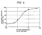
- Fig. 4 is a graph to show the relation between oxygen permeability at 25°C/90%RH of the surface protecting film and yellowing recovery factor of the surface covering member.
- the relation between oxygen permeability and yellowing recovery factor was obtained as follows. A lamination was formed on slide glass in such a structure that the outermost surface was an organic resin film as the surface protecting film and that an EVA resin containing the nonwoven fabric of glass fiber was sealed between the slide glass and the organic resin film.
- the EVA resin containing glass fibers corresponds the surface sealant resin layer in the solar cell module of the present invention. This lamination was subjected to a thermal degrading test at 150°C and for 15 hours.
- the thermal degrading test showed that yellowing of the sealant resin layer took place to greatly decrease the optical transmittance and that the decrease was equivalent to an almost 10% drop in output of solar cell module. Then it was exposed to ultraviolet rays under the output of 100 mW/cm 2 in the wavelength range of 300 to 400 nm by use of a metal halide lamp.
- the yellowing recovery factor is defined as a relative value when the optical transmittance (at wavelength 400 nm) immediately after the thermal degrading test is determined to be 0 and when the transmittance (at wavelength 400 nm) immediately after fabrication of the lamination is determined to be 100%.
- the sealant resin layer is normally crosslinked by radicals produced by thermal decomposition of an organic peroxide.
- a small amount of the organic peroxide usually remains in the sealant resin layer without being decomposed completely. Since the organic peroxide has the action to promote the yellowing of sealant resin layer, the remaining amount thereof after crosslinking of sealant resin should be preferably controlled as small as possible.
- Increasing the oxygen permeability of surface protecting film makes possible volatilization of the remaining organic peroxide through the surface protecting film and thus results in further enhancing the yellowing suppressing effect.
- the oxygen permeability of the surface protecting film needs to be not more than 50 cc/m 2 ⁇ 24 hr ⁇ atm. More specifically, the water vapor permeability of the surface protecting film is more preferably 20 g/m 2 ⁇ 24 hr or less at 40°C/90%RH. The lower limit of water vapor permeability of the surface protecting film is more preferably 1.0 g/m 2 ⁇ 24 hr at 40°C/90%RH.
- Materials suitably used for the surface protecting film 103 are, for example, fluoride polymers and acrylic resins.
- the fluoride polymers are favorably used, because they are excellent in the weathering resistance and pollution resistance.
- Specific examples include polyvinylidene fluoride resins, polyvinyl fluoride resins, and tetrafluoroethylene-ethylene copolymers.
- the polyvinylidene fluoride resins are excellent in terms of the weathering resistance, while the tetrafluoroethylene-ethylene copolymers are excellent in terms of compatibility of the weathering resistance and mechanical strength, and transparency.
- the surface protecting film 103 needs to have some thickness for securing the mechanical strength, but too great thicknesses are not preferred from the viewpoint of cost. Specifically, the thickness is preferably 20-200 ⁇ m and more preferably 30-100 ⁇ m.
- one surface of the surface protecting film 103 is preferably treated by a surface treatment such as the corona treatment, plasma treatment, ozone treatment, UV irradiation, electron beam irradiation, or flame treatment.
- a surface treatment such as the corona treatment, plasma treatment, ozone treatment, UV irradiation, electron beam irradiation, or flame treatment.
- the corona discharge treatment is preferably used, because its treatment rate is large and it can increase the adhesive force greatly by a relatively simple device.
- the surface sealant resin layer 102 is necessary for covering unevenness of photovoltaic element 101 with a resin, for protecting the photovoltaic element 101 from severe external circumstances such as temperature change, humidity, and impact, and for securing adhesion between the surface protecting film 103 and the photovoltaic element 101. Therefore, it needs to be excellent in the weathering resistance, adhesion, filling property, heat resistance, low temperature resistance, and impact resistance.
- Resins to meet these requirements include, for example, polyolefin based resins such as ethylene-vinyl acetate copolymers (EVA), ethylene-methylacrylate copolymers (EMA), ethylene-ethylacrylate copolymers (EEA), and polyvinyl butyral resins, urethane resins, silicone resins, and fluororesins.
- EVA ethylene-vinyl acetate copolymers
- EMA ethylene-methylacrylate copolymers
- EAA ethylene-ethylacrylate copolymers
- polyvinyl butyral resins polyvinyl butyral resins
- urethane resins silicone resins
- fluororesins fluororesins
- the surface sealant resin layer is preferably crosslinked in order to enhance the heat resistance and the crosslinking is more preferably controlled so as to achieve the gel percentage of 70 wt% or more.
- the crosslinking is more preferably controlled so as to achieve the gel percentage of 70 wt% or more.
- EVA it is preferably crosslinked with the organic peroxide, which can effectively prevent deformation or creep under use at high temperatures.
- the crosslinking with the organic peroxide is made in such a way that free radicals produced from the organic peroxide draw hydrogen and halogen atoms in the resin to form C-C bonds.
- the known methods for activating the organic peroxide include thermal decomposition, redox decomposition, and ion decomposition. In general, the thermal decomposition method is favorably adopted.
- Specific examples of the organic peroxide include, for example, hydroperoxide, dialkyl (allyl) peroxide, diacyl peroxide, peroxy ketal, peroxy ester, peroxy carbonate, ketone peroxide, and so on.
- An amount of the organic peroxide added is preferably 0.5 to 5 parts by weight relative to 100 parts by weight of the surface sealant resin.
- the resins used for the surface sealant resin layer 102 are those excellent in the weathering resistance, but an ultraviolet absorbing agent may also be added in order to further enhance the weathering resistance or in order to protect the layer located below the surface sealant resin layer.
- the ultraviolet absorbing agent can be selected from known compounds and is selected preferably from low-volatile ultraviolet absorbing agents in consideration of use environments of solar cell module. Specific examples of such agents are various organic compounds including salicylic acid based compounds, benzophenone based compounds, benzotriazole based compounds, and cyanoacrylate based compounds.
- the surface sealant resin layer 102 will become stabler to light.
- Typical examples of the light stabilizer are hindered amine based light stabilizers.
- the hindered amine based light stabilizers do not absorb the ultraviolet light, different from the ultraviolet absorbing agent, but they demonstrate a great synergistic effect when used with the ultraviolet absorbing agent.
- Contents of the above ultraviolet absorbing agent and light stabilizer added are preferably 0.1-1.0 wt% and 0.05-1.0 wt%, respectively, to the surface sealant resin.
- a thermal oxidation inhibitor may be added for improving the thermal resistance and thermal processability.
- the thermal oxidation inhibitor may be selected, for example, from monophenol based compounds, bisphenol based compounds, polymer type phenol based compounds, sulfur based compounds, and phosphoric acid based compounds.
- a content of the thermal oxidation inhibitor added is preferably 0.05-1.0 wt% to the surface sealant resin.
- a silane coupling agent or an organic titanate compound can be added to the surface sealant resin, for further enhancing adhesion between the glass fibers 106 described below and the surface sealant resin. It also presents an effect to enhance the adhesive force between the surface sealant resin layer 102 and the photovoltaic element 101 or the surface protecting film 103.
- An amount of the addition is preferably 0.1-3 parts by weight and more preferably 0.25-1 part by weight to 100 parts by weight of the surface sealant resin.
- the surface sealant resin layer 102 needs to be transparent in order to control decrease in quantity of light reaching the photovoltaic element 101 to as low level as possible.
- the optical transmittance thereof is preferably 80% or more and more preferably 90% or more in the visible light wavelength region of 400 nm inclusive to 800 nm inclusive.
- the refractive index of the surface sealant resin layer 102 at 25°C is preferably between 1.1 and 2.0 and more preferably between 1.1 and 1.6.
- EVA sheets for solar cell in a sheet form of EVA containing the above additives are commercially available.
- Examples of such commercially available EVA sheets are solar EVA from Hisheet Kogyo Kabushiki Kaisha, EVASAFE WG series from BRIDGESTONE CORP., PHOTOCAP from SPRINGBORN LABORATORIES INC., and so on.
- One selected from these is put between the photovoltaic element 101 and the surface member such as the surface protecting film 103 and they are pressed under heat, whereby the solar cell module can be fabricated readily.
- the surface sealant resin layer 102 preferably contains the glass fiber nonwoven fabric 106.
- the glass fiber nonwoven fabric 106 has a function to help degassing from spaces in the solar cell module lamination in a vacuuming step in a vacuum lamination process and a function to prevent the surface sealant resin from flowing to the module edges to thin the surface sealant resin layer 102, as being impregnated in the surface sealant resin of EVA or the like melted in a heating step. Further, since the glass fiber nonwoven fabric 106 is impregnated in the surface sealant resin, it also functions as a reinforcing material of the surface sealant resin layer 102, thereby presenting an effect to make it harder for a flaw in the surface to propagate to the photovoltaic element 101.
- the glass fiber nonwoven fabric 106 is obtained by binding glass fibers with a binder resin.
- the binder resin may be selected, for example, from acrylic resins, urethane resins, polyvinyl alcohol resins, polyester resins, and EVA resins, and it is selected preferably from the acrylic resins in terms of the heat resistance.
- a rate of the glass fiber nonwoven fabric 106 to the surface sealant resin is preferably 1-30 parts by weight and more preferably between 5-20 parts by weight to 100 parts by weight of the surface sealant resin. If the rate is below one part by weight, there is such a tendency that the surface covering member is unlikely to have sufficient scratch resistance. If the rate is over 30 parts by weight, an amount of glass fibers will be excessive to the surface sealant resin, which will cause failure of appearance, because the glass fiber nonwoven fabric is not impregnated well in the surface sealant resin in the module lamination step or which will readily raise a problem of poor appearance or separation of glass fibers from the surface sealant resin layer 102 in long-term outdoor exposure.
- the surface of the surface covering member is often provided with unevenness in consideration of decrease of reflected light, suppression of occurrence of wrinkle upon lamination, design, and so on.
- the maximum level difference between adjacent depressed and projected portions of the unevenness is preferably between 5 ⁇ m inclusive and 100 ⁇ m inclusive. If the maximum level difference is below 5 ⁇ m, there is such a tendency that the effect of provision of the unevenness cannot be demonstrated well. If the maximum level difference is over 100 ⁇ m, the surface sealant resin layer 102 will be locally thin in depressed portions where the amount of glass fibers tends to be excessive to the surface sealant resin.
- This unevenness may be formed during a cover forming step or may be formed by a method of pressing or the like after formation of cover.
- the back sealant resin layer 104 is given for adhesion between the photovoltaic element 101 and the back covering film 105.
- Preferred materials for the back sealant resin layer 104 are those capable of securing sufficient adhesion to the substrate, excellent in long-term durability, resistant to thermal expansion and thermal contraction, and flexible.
- Preferably used materials are, for example, resins including hot melt materials such as EVA, EEA, or polyvinyl butyral, and epoxy adhesives having flexibility, and two sided adhesive tapes. It is a matter of course that the back sealant resin layer 104 can also be made of the same material as the surface sealant resin layer 102, which is normally the case in many applications.
- the back covering film 105 is necessary for maintaining electrical insulation between the substrate of the photovoltaic element 101 and the outside.
- Preferred materials are those capable of securing sufficient electrical insulation to the substrate, excellent in long-term durability, resistant to thermal expansion and thermal contraction, and flexible.
- Suitably applicable films are, for example, films of nylons and polyethylene terephthalate. It is also possible to use a lamination film in which the back sealant resin 104 and back covering film 105 described above are preliminarily stacked together.
- the module backing may be adhered to the outside of back covering film 105 in order to increase the mechanical strength of solar cell module or in order to prevent distortion or warpage due to temperature change.
- the backing 107 is preferably selected, for example, from steel sheets, plastic sheets, FRP (glass fiber reinforced plastics) sheets, or flexible resin sheets.
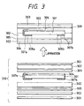
- a building material such as a wall material or a roofing material incorporating the solar cell can be made by folding it.
- Figs. 5A-5C show examples of roofing materials according to the present invention.
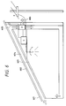
- Fig. 5A shows a roofing material of a type where ridge-side connecting portion 501 and eaves-side connecting portion 502 are semi-jointed with each other.
- Fig. 5B shows a roofing material of a type where engaging portions thereof 505 are fitted in fixing members 504 fixed on sheathing roof board 503.
- Fig. 5C shows roofing materials connecting parts of which are covered by caps 507 after adjacent roofing materials are connected at connecting parts thereof 506 by the fixing members.
- a photovoltaic element 500 is provided in a light receiving surface of each roofing material in the examples shown.
- FIG. 6 An air circulation system can be constructed as shown in Fig. 6 by use of these roofing materials.
- Fig. 6 shows an example of application of the aforementioned combination solar cell and roofing member to the air circulation system of house.
- Arrows in the drawing indicate flows of air and the external air taken in through eave part 601 is guided in space 604 between roofing materials 602 and roof underlayment 603 to be taken through ridge part 605 into the house.
- a fan F is provided midway of air flow path to circulate the air. In the cold season the air warmed up in the space 604 is taken into the room and in the hot season the air is discharged through exhaust port 606 to the outside, thereby enhancing heat insulation performance of roof.
- a heat accumulating device may be provided below the floor.
- Power generated in the combination solar cell and roofing members 602 is led through the ridge into the house and then to inverter I, thus constituting a solar electric power generation system.
- the output from the solar electric power generation system may be consumed at load L such as a lamp or may be sent to the commercial electrical power system E.
- the photovoltaic element 101 employed in the present invention can be made of a monocrystalline, polycrystalline, microcrystalline, or amorphous semiconductor.
- the material is selected from silicon based or compound based semiconductor materials.
- a typical example of the photovoltaic element 101 according to the present invention is a one obtained by forming a nonmonocrystalline semiconductor photoactive layer and a transparent, conductive layer on a substrate.
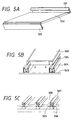
- Figs. 2A and 2B are views to show the schematic structure of the example.
- Fig. 2A is a cross-sectional view and
- Fig. 2B is a top plan view of the light receiving surface side.
- reference numeral 201 designates a substrate, 202 a back reflecting layer, 203 a semiconductor photoactive layer, 204 a transparent, conductive layer, 205 a collector electrode pattern, and 206 output terminals.
- the substrate 201 functions as a substrate of photovoltaic element and also functions as a lower electrode.
- the substrate 201 may be made of a material selected, for example, from silicon, tantalum, molybdenum, tungsten, stainless steel, aluminum, copper, titanium, carbon sheet, galvanized sheet iron, or resin films or ceramics on which a conductive layer of metal or metallic oxide is formed.
- a metal layer, or a metallic oxide layer, or a combination of the metal layer and metallic oxide layer may be formed as a back reflecting layer 202 on the substrate 201.
- the metal layer is, for example, of Ti, Cr, Mo, W, Al, Ag, or Ni and the metallic oxide layer is, for example, of ZnO, TiO 2 , or SnO 2 .
- the back reflecting layer 202 can be made by a method selected from the resistance heating vapor deposition method, the electron beam vapor deposition method, the sputtering method, and so on.
- the semiconductor photoactive layer 203 is a section for undergoing photoelectric conversion.
- materials for the semiconductor photoactive layer 203 include nonmonocrystalline semiconductors such as pn junction type polycrystalline silicon materials or pin junction type amorphous silicon materials, and compound semiconductors including CuInSe 2 , CuInS 2 , GaAs, CdS/Cu 2 S, CdS/CdTe, CdS/InP, and CdTe/Cu 2 Te.
- the nonmonocrystalline semiconductors are preferably used and amorphous silicon is more preferred.
- the semiconductor photoactive layer 203 may be made by sheeting of molten silicon or by a heat treatment of amorphous silicon in the case of polycrystalline silicon; or by a plasma enhanced CVD method using silane gas or the like as a raw material in the case of amorphous silicon; or by ion plating, ion beam deposition, vacuum vapor deposition, sputtering, or electrodeposition in the case of the compound semiconductors.
- the transparent, conductive layer 204 serves as an upper electrode of the photovoltaic element.
- the transparent, conductive layer 204 may be made of a material selected, for example, from In 2 O 3 , SnO 2 , In 2 O 3 -SnO 2 (ITO), ZnO, TiO 2 , Cd 2 SnO 4 , and crystalline semiconductors doped with a high concentration of impurities.
- a method for forming the transparent, conductive layer 204 may be selected from the resistance heating vapor deposition, sputtering, spraying, CVD, and impurity diffusion method.
- the collector electrode 205 (grid) of a grating pattern may be provided on the transparent, conductive layer 204, for efficiently collecting electric currents.
- Specific materials for the collector electrode 205 are, for example, Ti, Cr, Mo, W, Al, Ag, Ni, Cu, Sn, or conductive pastes including a silver paste.
- the conductive pastes usually used are those wherein fine powder of silver, gold, copper, nickel, or carbon is dispersed in a binder polymer.
- the binder polymer is selected, for example, from polyester, epoxy, acrylic, alkyd, polyvinyl acetate, rubber, urethane, and phenol resins.
- a method for making the collector electrode 205 may be selected from sputtering with a mask pattern, resistance heating, the CVD process, a method for first evaporating a metal film over the entire surface and thereafter patterning it by removing unnecessary portions by etching, a method for directly forming the grid electrode pattern by photo-CVD, a method for first forming a mask of a negative pattern of the grid electrode pattern and then performing plating thereon, a method for printing a conductive paste, and a method for bonding metal wires with a conductive paste.
- the output terminals 206 are attached to the substrate 201 and to the collector electrode 205, for taking out the electromotive force.
- Metal member 206b of a belt shape, for example, of copper is joined with the substrate 201 by soldering 208 or is electrically connected therewith by spot welding with laser.
- Metal member 206a of a belt shape, for example, of copper is electrically connected with the collector electrode 205 by conductive paste 207 or by soldering.
- Photovoltaic elements produced by the above techniques are connected in series or in parallel, depending upon desired voltage or electric current.
- Another arrangement may be such that photovoltaic elements are integrated on an insulated substrate to achieve desired voltage or current.
- the transparent, rigid, organic resin thin film layer 108 may be provided on the light incidence side of the photovoltaic element in order to present humidity resistance or scratch resistance.
- materials for the layer 107 are acrylic resins, silicone resins, acryl silicone resins, polyalkoxy silane resins, fluororesins, polyester resins, urethane resins, epoxy resins, alkyd resins, polysilazane resins, and so on.
- Materials preferred in view of weathering resistance are the acrylic resins, silicone resins, acryl silicone resins, and fluororesin. More preferred materials are resins mainly containing the acrylic resin or the acryl silicone resin. These resins are preferably crosslinked to enhance heat resistance in consideration of use of solar cell module at high temperatures. A method for crosslinking is selected from normal methods using the organic peroxide or isocyanate.
- a normal method for covering the light receiving surface of photovoltaic element 101 by the surface sealant resin layer 102, the surface protecting film 103, and the glass fiber nonwoven fabric 106 is a method for forming a sheet of surface sealant resin and heat-pressing it on the photovoltaic element 101 together with the surface protecting film 103 and glass fiber nonwoven fabric 106.
- the solar cell module can be made by heat-pressing a stack in which the surface sealant resin sheet and glass fiber nonwoven fabric 106 are interposed between the photovoltaic element 101 and the surface protecting film 103. At this time, if a member having an uneven shape is placed outside of the surface protecting film 103 and is arranged to be urged against the surface protecting film 103 upon pressing, unevenness can be made readily in the surface of surface covering member.
- Heating temperature and heating time upon pressing may be determined as occasion may demand.
- the surface sealant resin layer is of a crosslinked resin, they can be determined by the temperature and time for allowing sufficient progress of crosslinking reaction, specifically, by thermal decomposition temperature characteristics of the organic peroxide.
- heat pressing is completed by the temperature and time for permitting progress of 90% of thermal decomposition and, more preferably, progress of 95% or more of thermal decomposition.
- the back surface covering may be made using the back covering film 105 and back sealant resin by the same method. Since the surface sealant resin and the back sealant resin are normally the same material, the back covering step can be carried out at the same time as the above step.
- the solar cell module can be made by stacking the surface protecting film 103/the surface sealant resin sheet/the glass fiber nonwoven fabric 106/the photovoltaic element 101/the back sealant resin sheet/the back covering film 105 in this order to form a solar cell module laminate and heat-pressing it.
- the surface sealant resin sheet is melted by heating to take the glass fibers 106 into the inside thereof, thus becoming the surface sealant resin 102.
- the back sealant resin sheet is also melted by heating to become the back sealant resin 104 covering the back surface of photovoltaic element 101.
- a method for heat pressing may be selected from a variety of conventionally known methods such as vacuum lamination or roll lamination.
- the solar cell module of the present invention preferably has the maximum use temperature of 70°C or more. This permits us to expect an effect of recovery from light degradation, particularly, of amorphous semiconductor and also permits us to enjoy the maximum yellowing suppressing effect of the surface sealant resin layer purposed by the present invention.
- the solar cell modules were put in an ultraenergy irradiation test machine (available from Suga Shikenki) to be subjected to a due cycle test for repeating exposure to ultraviolet light for five hours with a metal halide lamp (exposure intensity: 100 mW/cm 2 at 300 nm-400 nm, atmosphere: black panel temperature 70°C/humidity 70%RH) and dew condensation (temperature 30°C/humidity 96%RH) for one hour, and then change in the appearance was observed after 2000 hours. Observation results were indicated by ⁇ for no change and a brief comment of condition for some change.
- the solar cell modules were put in a sunshine weatherometer (available from Suga Shikenki) to be subjected to an accelerated weathering test for repeating 8-minute showers every two hours with exposure to light (exposure intensity: 3 SUN, atmosphere: black panel temperature 83°C/humidity 50%RH) with a xenon lamp, and change in the appearance was observed after 5000 hours. Observation results were indicated by ⁇ for no change and by a brief comment of condition for some change.
- the solar cell modules were put in an environmental test machine to be kept still under the circumstances of temperature 85°C/humidity 85%RH for 1000 hours, and change in the appearance was observed. Observation results were indicated by ⁇ for no change and by a brief comment of condition for some change.
- Amorphous silicon (a-Si) photovoltaic elements having the structure shown in Figs. 2A and 2B were fabricated in the following procedures.
- An Al layer (5000 ⁇ thick) and a ZnO layer (5000 ⁇ thick) were successively made as the back reflecting layer 202 on the cleaned stainless steel substrate 201 by sputtering.
- tandem type a-Si semiconductor photoactive layer 203 was made in the layer structure of n-layer 150 ⁇ thick/i-layer 4000 ⁇ thick/p-layer 100 ⁇ thick/n-layer 100 ⁇ thick/i-layer 800 ⁇ thick/p-layer 100 ⁇ thick by making the n-type a-Si layers from mixture gas of SiH 4 , PH 3 , and H 2 , the i-type a-Si layers from mixture gas of SiH 4 and H 2 , and the p-type microcrystalline ⁇ c-Si layers from mixture gas of SiH 4 , BF 3 , and H 2 by the plasma enhanced CVD process.
- a thin film of In 2 O 3 (700 ⁇ thick) was made as the transparent, conductive layer 204 by evaporating In under an O 2 atmosphere by the resistance heating method.
- the grid electrode lines as the collector electrode 205 were made by screen printing of silver paste, a copper tab as the minus output terminal 206b was attached to the substrate 201 with stainless soldering 208, and a tape of tin foil as the plus output terminal 206a was attached to the collector electrode 205 with a conductive adhesive 207, thus obtaining the photovoltaic element.
- the plus output terminal 206a was routed through an insulator to the back side and the output was arranged to be taken out through holes of the back covering member described below. A plurality of photovoltaic elements were made in this way.
- the transparent, rigid, organic resin thin film layer 304 was made as follows. A solution was prepared by adding 2.8 parts by weight of ⁇ -metacryloxy propyltrimetoxy silane (trade name: SH6040, available from Toray Dow Corning Silicone Inc.) as a silane coupling agent to 100 parts by weight of a coating (trade name: Fine Hard N36-21F, resin solid content 30%, available from Showa Technocoat) in which an acrylic resin, an inorganic polymer, and hexamethylene diisocyanate blocked by ⁇ -caprolactam were uniformly dissolved or dispersed in an organic solvent. The solution was applied by an airless spray to the light receiving surface of photovoltaic element 301 and the surface was heated at 200°C for ten minutes to evaporate the solvent and to crosslink the resin, thus making the transparent, rigid, organic resin thin film layer 304.
- ⁇ -metacryloxy propyltrimetoxy silane trade name: SH6040, available from Toray Dow Corning Silicone Inc.
- a coating trade name: Fine
- the solar cell module lamination 310 was made by stacking the photovoltaic element 301, a glass fiber nonwoven fabric 309 (trade name: Glassper, basis weight 80 g/m 2 , available from Honshu Seishi), an EVA sheet as the sealant resin layer 302 (trade name: PHOTOCAP, thickness 460 ⁇ m, available from SPRINGBORN LABORATORIES INC.), a non-oriented ETFE film having a corona-discharge-treated surface as the surface protecting film 303 (trade name: TEFZEL film, thickness 50 ⁇ m, available from DuPont Inc.), a nylon film as the back covering film 305 (trade name: Dertec, thickness 63.5 ⁇ m, available from DuPont Inc.), and a galvanized sheet ion as the module backing 306 (trade name: Taima color GL, thickness 0.27 mm, available from Daido Kohan) in the order of ETFE/EVA/glass fiber nonwoven fabric/element/EVA/nylon/EVA/stee
- a stainless mesh 40 ⁇ 40 meshes, diameter of line 0.15 mm
- a fluorocarbon film for release (trade name: Teflon PFA film, thickness 50 ⁇ m, available from DuPont Inc.) outside of the surface protecting film 303, and the lamination was heat-pressed at 150°C for 30 minutes while degassing under pressure with a vacuum laminator, thereby obtaining the solar cell module.
- the rate of glass fiber nonwoven fabric was 8.7 parts by weight to 100 parts by weight of the surface sealant resin in the surface covering member of this solar cell module.
- the unevenness having the maximum level difference of 30 ⁇ m was formed in the surface of surface covering member by the mesh.
- the EVA sheet used for the sealant resin layer 302 is the one popularly used as a sealant of solar cell, in which 1.5 parts by weight of the organic peroxide as a crosslinking agent, 0.3 part by weight of the ultraviolet absorbing agent, 0.1 part by weight of the light stabilizer, 0.2 part by weight of the thermal oxidation inhibitor, and 0.25 part by weight of the silane coupling agent are blended to 100 parts by weight of the EVA resin (the content of vinyl acetate: 33%).
- the binder resin of the glass fiber nonwoven fabric 309 is the acrylic resin.
- the output terminal 307a was preliminarily routed to the back surface of photovoltaic element 301, whereby after the lamination, the output was able to be taken out from the output terminals 307a and 307b through terminal outlets 308a, 308b preliminarily perforated in the module backing 306.
- the oxygen permeability of the surface protecting film 303 used herein was 15 cc/m 2 ⁇ 24 hr ⁇ atm at 25°C/90%RH and the water vapor permeability thereof was 11.5 g/m 2 ⁇ 24 hr at 40°C/90%RH.
- a PCTFE (polychlorotrifluoroethylene) film (trade name: Neofron CTFE, thickness 50 ⁇ m, available from Daikin Kogyo) was used as the surface protecting film 303.
- the PCTFE film is known as a resin having a small gas permeability among the fluororesin films.
- the oxygen permeability and water vapor permeability of the PCTFE film used herein were measured.
- the oxygen permeability thereof was 0.5 cc/m 2 ⁇ 24 hr ⁇ atm at 25°C/90%RH and the water vapor permeability thereof was 0.3 g/m 2 ⁇ 24 hr at 40°C/90%RH.
- Example 2 In place of the ETFE film in Example 1, a white sheet of tempered glass for solar cell (trade name: Solatex, thickness 3.2 mm, available from AFG Inc.) was used as the surface protecting material. Using an aluminum laminate Tedlar film (available from Tokai Almi Haku) instead of the sheet ion on the back surface, the solar cell module lamination was made in the stacking order of glass/EVA/glass fiber nonwoven fabric/element/EVA/aluminum laminate Tedlar film. Then this lamination was placed with the glass down in the vacuum laminator and was heat-pressed at 150°C for 30 minutes while degassing under pressure, thereby obtaining the solar cell module.
- Tedlar film available from Tokai Almi Haku
- glass has the oxygen permeability and the water vapor permeability of zero. It is thus considered that there is no supply of oxygen to the surface sealant resin layer and no volatilization of remaining organic peroxide from the surface sealant resin layer.
- the solar cell module was fabricated in the same manner as in Example 1 except that the glass fiber nonwoven fabric 309 in Example 1 was replaced by another (trade name: Craneglass, basis weight 80 g/m 2 , available from Crane and Co., Inc.) containing the binder resin of polyvinyl alcohol.
- the solar cell module was fabricated in the same manner as in Comparative Example 1-2 except that the glass fiber nonwoven fabric 309 in Comparative Example 1-2 was replaced by the one containing the binder resin of polyvinyl alcohol (trade name: Craneglass, basis weight 80 g/m 2 , available from Crane and Co., Inc.).
- the binder resin of polyvinyl alcohol trade name: Craneglass, basis weight 80 g/m 2 , available from Crane and Co., Inc.
- An EEA resin (the content of ethylacrylate: 25%) formed in a sheet form was used as the sealant resin layer 302 in Example 1.
- Blended in this resin were 1.5 parts by weight of the organic peroxide as the crosslinking agent, 0.3 part by weight of the ultraviolet absorbing agent, 0.1 part by weight of the light stabilizer, 0.2 part by weight of the thermal oxidation inhibitor, 0.25 part by weight of the silane coupling agent, and 3.0 parts by weight of triallyl isocyanurate as the crosslinking agent.
- the solar cell module was fabricated in the same manner as in Example 1 except for the above.
- the EEA resin (the content of ethylacrylate: 25%) formed in the sheet form was used as the sealant resin layer 302 in Comparative Example 1-2.
- the solar cell module was fabricated in the same manner as in Comparative Example 1-2 except for the above.
- Example 1 The thickness of the ETFE film in Example 1 was changed to 12 ⁇ m.
- the solar cell module was fabricated in the same manner as in Example 1 except for it.
- the oxygen permeability and water vapor permeability of the ETFE film as the surface protecting film used herein were measured, which showed that the oxygen permeability was 60 cc/m 2 ⁇ 24 hr ⁇ atm at 25°C/90%RH and the water vapor permeability was 43 g/m 2 ⁇ 24 hr at 40°C/90%RH.
- a solar cell module is constructed in such an arrangement that a photovoltaic element is covered by at least a sealant resin and a surface protecting film, wherein an oxygen permeability of the surface protecting film is not less than 1 cc/m 2 ⁇ 24 hr ⁇ atm and not more than 50 cc/m 2 ⁇ 24 hr ⁇ atm at 25°C/90%RH, thereby providing the solar cell module with high reliability free of deterioration of the sealant resin, particularly free of yellowing, in long-term outdoor exposure use.
Landscapes
- Engineering & Computer Science (AREA)
- Structural Engineering (AREA)
- Civil Engineering (AREA)
- Architecture (AREA)
- General Physics & Mathematics (AREA)
- Computer Hardware Design (AREA)
- Microelectronics & Electronic Packaging (AREA)
- Power Engineering (AREA)
- Physics & Mathematics (AREA)
- Electromagnetism (AREA)
- Condensed Matter Physics & Semiconductors (AREA)
- Photovoltaic Devices (AREA)
- Sealing Material Composition (AREA)
Applications Claiming Priority (2)
| Application Number | Priority Date | Filing Date | Title |
|---|---|---|---|
| JP266824/96 | 1996-10-08 | ||
| JP8266824A JPH10112549A (ja) | 1996-10-08 | 1996-10-08 | 太陽電池モジュール |
Publications (2)
| Publication Number | Publication Date |
|---|---|
| EP0836233A2 true EP0836233A2 (fr) | 1998-04-15 |
| EP0836233A3 EP0836233A3 (fr) | 1999-01-20 |
Family
ID=17436175
Family Applications (1)
| Application Number | Title | Priority Date | Filing Date |
|---|---|---|---|
| EP97117145A Withdrawn EP0836233A3 (fr) | 1996-10-08 | 1997-10-02 | Module de cellules solaires |
Country Status (5)
| Country | Link |
|---|---|
| US (1) | US6307145B1 (fr) |
| EP (1) | EP0836233A3 (fr) |
| JP (1) | JPH10112549A (fr) |
| KR (1) | KR100350594B1 (fr) |
| CN (1) | CN1145220C (fr) |
Cited By (12)
| Publication number | Priority date | Publication date | Assignee | Title |
|---|---|---|---|---|
| EP1054456A2 (fr) * | 1999-05-17 | 2000-11-22 | Dai Nippon Printing Co., Ltd. | Couche de protection pour un module de cellules solaires, sa méthode de fabrication et module de cellules solaires |
| US6693237B2 (en) | 2000-05-23 | 2004-02-17 | Canon Kabushiki Kaisha | Sealing composition for sealing solar cell, and solar cell module and building material-integral type solar cell module using said composition |
| US7309831B2 (en) | 1998-10-13 | 2007-12-18 | Dai Nippon Printing Co., Ltd | Protective sheet for solar battery module, method of fabricating the same and solar battery module |
| WO2010008446A2 (fr) * | 2008-06-25 | 2010-01-21 | Ip Dynamics, Llc | Panneau solaire résistant à l’humidité et son procédé de fabrication |
| EP2308633A1 (fr) * | 2009-10-07 | 2011-04-13 | Asociación Industrial de Óptica, Color e Imagen - AIDO | Dispositif de fixation pour soudure au laser de contacts électriques dans des piles photovoltaïques |
| WO2011073303A3 (fr) * | 2009-12-17 | 2012-06-21 | Designergy Sa | Elément de construction sensiblement bidimensionnel |
| EP3387335A1 (fr) * | 2015-12-10 | 2018-10-17 | Flisom AG | Ensemble photovoltaïque doté de structure de montage intégrée et son procédé de fabrication |
| EP3416200A4 (fr) * | 2016-08-18 | 2019-07-24 | Tiger New Surface Materials (Suzhou) Co., Ltd. | Matériau d'encapsulation pour module photovoltaïque et procédé de préparation de matériau d'encapsulation |
| IT201800007626A1 (it) * | 2018-07-30 | 2020-01-30 | Glass Project Srls | Pannello multistrato per il rivestimento di superfici esterne di un edificio |
| CN112928183A (zh) * | 2021-01-22 | 2021-06-08 | 徐州中辉光伏科技有限公司 | 一种晶硅电池背面n层膜贴合设备 |
| GB2593119A (en) * | 2019-02-21 | 2021-09-22 | Teodoro Martins Alexander | Lightweight encapsulated composite photovoltaic panel |
| EP4276916A1 (fr) * | 2022-05-09 | 2023-11-15 | Das Energy Limited | Panneau photovoltaïque et procédé de fabrication d'un panneau photovoltaïque |
Families Citing this family (56)
| Publication number | Priority date | Publication date | Assignee | Title |
|---|---|---|---|---|
| DE60011544T2 (de) * | 1999-10-28 | 2005-09-15 | Bridgestone Corp. | Verfahren zum Oberflächenbehandeln und Kaschieren eines fluorhaltigen Harzes |
| JP4036616B2 (ja) * | 2000-01-31 | 2008-01-23 | 三洋電機株式会社 | 太陽電池モジュール |
| KR100830798B1 (ko) * | 2000-06-15 | 2008-05-20 | 아크조 노벨 엔.브이. | 제거 가능한 최상층을 갖는 태양 전지 유닛 |
| US7053294B2 (en) * | 2001-07-13 | 2006-05-30 | Midwest Research Institute | Thin-film solar cell fabricated on a flexible metallic substrate |
| US6670540B2 (en) * | 2001-10-10 | 2003-12-30 | Ecosol Solar Technologies Ltd. | Photovoltaic strip assembly |
| AU2002301252B2 (en) * | 2001-10-12 | 2007-12-20 | Bayer Aktiengesellschaft | Photovoltaic modules with a thermoplastic hot-melt adhesive layer and a process for their production |
| DE10255964A1 (de) * | 2002-11-29 | 2004-07-01 | Siemens Ag | Photovoltaisches Bauelement und Herstellungsverfahren dazu |
| JP4401649B2 (ja) * | 2002-12-13 | 2010-01-20 | キヤノン株式会社 | 太陽電池モジュールの製造方法 |
| JP2004288898A (ja) * | 2003-03-24 | 2004-10-14 | Canon Inc | 太陽電池モジュールの製造方法 |
| JP2004289034A (ja) * | 2003-03-25 | 2004-10-14 | Canon Inc | 酸化亜鉛膜の処理方法、それを用いた光起電力素子の製造方法 |
| US7534956B2 (en) * | 2003-04-10 | 2009-05-19 | Canon Kabushiki Kaisha | Solar cell module having an electric device |
| JP2004319812A (ja) * | 2003-04-17 | 2004-11-11 | Canon Inc | 電力変換器付き太陽電池モジュール |
| JP2004319800A (ja) * | 2003-04-17 | 2004-11-11 | Canon Inc | 太陽電池モジュール |
| JP4779074B2 (ja) * | 2003-10-03 | 2011-09-21 | 三井・デュポンポリケミカル株式会社 | 太陽電池封止材用シート |
| JP4157459B2 (ja) * | 2003-10-30 | 2008-10-01 | シャープ株式会社 | 軽量太陽電池モジュールとその製造方法 |
| JP2005150318A (ja) * | 2003-11-14 | 2005-06-09 | Canon Inc | 太陽電池モジュール及びその製造方法 |
| JP2005175197A (ja) * | 2003-12-11 | 2005-06-30 | Canon Inc | 太陽電池モジュール及びその製造方法 |
| JP4681806B2 (ja) * | 2003-12-19 | 2011-05-11 | キヤノン株式会社 | 太陽電池モジュール |
| JP2005183660A (ja) * | 2003-12-19 | 2005-07-07 | Canon Inc | 太陽電池モジュール |
| JP4890752B2 (ja) * | 2004-08-27 | 2012-03-07 | キヤノン株式会社 | 太陽電池モジュール |
| JP4979103B2 (ja) | 2004-12-24 | 2012-07-18 | 三菱樹脂株式会社 | 太陽電池用ポリエステルフィルム |
| WO2006089044A2 (fr) * | 2005-02-16 | 2006-08-24 | Energy Conversion Devices, Inc. | Lamelle ignifuge et module photovoltaique incorporant le lamelle ignifuge |
| WO2008010814A2 (fr) * | 2005-08-05 | 2008-01-24 | Kahrl Retti | composition et procédé d'accumulation d'énergie solaire à multiples couches, BUCKMINSTERFULLERÈNE d'accumulation d'énergie solaire, dispositif de couplage inductif; châssis de véhicule; moteur hydrogène à admission atmosphérique; pneu générant de l'énergie électrique; et dispositif d'accumulation d'énergie mécanique |
| US20080276983A1 (en) * | 2005-11-04 | 2008-11-13 | Robert Andrew Drake | Encapsulation of Photovoltaic Cells |
| EP1997126A2 (fr) * | 2006-03-13 | 2008-12-03 | Nanogram Corporation | Silicium mince ou feuilles de germanium et photovoltaique forme a partir de feuilles minces |
| CN101454899B (zh) * | 2006-03-28 | 2012-05-02 | 索洛能源公司 | 光伏模块及其制造方法 |
| JP4667406B2 (ja) * | 2006-03-30 | 2011-04-13 | 三洋電機株式会社 | 太陽電池モジュール及びその製造方法 |
| JP5054326B2 (ja) * | 2006-05-01 | 2012-10-24 | 昭和シェル石油株式会社 | Cis系薄膜太陽電池モジュールの改良された耐久性試験方法 |
| US7666466B2 (en) * | 2006-05-03 | 2010-02-23 | Michael Gumm | Elastomeric waterproofing and weatherproofing photovoltaic finishing method and system |
| US20070256727A1 (en) * | 2006-05-03 | 2007-11-08 | Michael Gumm | Elastomeric Waterproofing and Weatherproofing Photovoltaic Finishing Method and System |
| US20080128018A1 (en) * | 2006-12-04 | 2008-06-05 | Richard Allen Hayes | Solar cells which include the use of certain poly(vinyl butyral)/film bilayer encapsulant layers with a low blocking tendency and a simplified process to produce thereof |
| KR100956145B1 (ko) * | 2007-03-21 | 2010-05-06 | 코오롱건설주식회사 | 아몰퍼스 실리콘 박막필름을 이용한 투광형 태양전지 복층모듈 |
| CA2693049A1 (fr) * | 2007-06-28 | 2009-01-08 | Certainteed Corporation | Tuiles photovoltaiques et procedes de fabrication associes |
| US20090032088A1 (en) * | 2007-08-03 | 2009-02-05 | Mario Rabinowitz | Sealants for Solar Energy Concentrators and Similar Equipment |
| JP2009146625A (ja) * | 2007-12-12 | 2009-07-02 | Sony Corp | 色素増感光電変換素子モジュールおよびその製造方法ならびに光電変換素子モジュールおよびその製造方法ならびに電子機器 |
| KR20090067350A (ko) * | 2007-12-21 | 2009-06-25 | 주성엔지니어링(주) | 박막형 태양전지 및 그 제조방법 |
| CN101582655B (zh) * | 2008-05-16 | 2013-05-08 | 鸿富锦精密工业(深圳)有限公司 | 具有太阳能电池的便携式电子装置 |
| JP2010041040A (ja) * | 2008-07-10 | 2010-02-18 | Semiconductor Energy Lab Co Ltd | 光電変換装置および光電変換装置の製造方法 |
| EP2308098B1 (fr) * | 2008-07-15 | 2012-02-01 | Dow Global Technologies LLC | Procédé de fabrication d'une structure laminée verre/film de polyoléfine |
| RU2011118375A (ru) | 2008-10-09 | 2012-11-20 | Асахи Гласс Компани, Лимитед (Jp) | Фторполимерная пленка темного типа и задний лист для модуля солнечного элемента |
| DE102008055969A1 (de) * | 2008-11-05 | 2010-06-10 | Sefar Ag | Substrat für eine optoelektronische Vorrichtung |
| US20110168238A1 (en) * | 2010-01-11 | 2011-07-14 | Solopower, Inc. | Flexible solar modules and manufacturing the same |
| FR2955705B1 (fr) * | 2010-01-27 | 2012-07-27 | Suez Environnement | Module de production d'energie mixte photovoltaique et thermique a partir du rayonnement solaire, et installation equipee de tels modules |
| JP2012054515A (ja) * | 2010-09-03 | 2012-03-15 | Fuji Electric Co Ltd | 太陽電池モジュールの製造方法 |
| KR101266103B1 (ko) * | 2010-09-29 | 2013-05-27 | 엘지전자 주식회사 | 태양 전지 모듈 및 그 제조 방법 |
| KR101063787B1 (ko) * | 2011-05-25 | 2011-09-08 | (주)솔라원 | 절연 특성이 개선된 태양광 발전용 모듈 |
| US20130153008A1 (en) * | 2011-12-15 | 2013-06-20 | E I Du Pont De Nemours And Company | Photovoltaic module |
| KR101307425B1 (ko) * | 2012-01-13 | 2013-09-11 | 도레이첨단소재 주식회사 | 태양광 모듈용 저수축 봉지재 시트 및 이를 이용한 태양광 모듈 |
| CN104334673B (zh) * | 2012-05-22 | 2017-08-01 | 积水化学工业株式会社 | 片状密封材料及层叠片状密封材料 |
| US9714756B2 (en) | 2013-03-15 | 2017-07-25 | Morgan Solar Inc. | Illumination device |
| US9960303B2 (en) | 2013-03-15 | 2018-05-01 | Morgan Solar Inc. | Sunlight concentrating and harvesting device |
| US9464782B2 (en) | 2013-03-15 | 2016-10-11 | Morgan Solar Inc. | Light panel, optical assembly with improved interface and light panel with improved manufacturing tolerances |
| US9595627B2 (en) | 2013-03-15 | 2017-03-14 | John Paul Morgan | Photovoltaic panel |
| WO2016137894A1 (fr) * | 2015-02-23 | 2016-09-01 | Sandia Solar Technologies Llc | Dispositifs et systèmes photovoltaïques solaires intégrés |
| EP3467880A4 (fr) * | 2016-05-31 | 2019-05-22 | Panasonic Intellectual Property Management Co., Ltd. | Module solaire et son procédé de fabrication |
| US11489488B2 (en) | 2018-04-13 | 2022-11-01 | Nextracker Llc | Light management systems for optimizing performance of bifacial solar module |
Citations (8)
| Publication number | Priority date | Publication date | Assignee | Title |
|---|---|---|---|---|
| EP0536738A2 (fr) * | 1991-10-08 | 1993-04-14 | Canon Kabushiki Kaisha | Module de cellules solaires avec caractéristiques améliorées de résistance atmosphérique |
| EP0577985A1 (fr) * | 1992-06-08 | 1994-01-12 | Kanegafuchi Kagaku Kogyo Kabushiki Kaisha | Module solaire en semi-conducteur amorphe ayant une passivation améliorée |
| US5389159A (en) * | 1992-09-01 | 1995-02-14 | Canon Kabushiki Kaisha | Solar cell module and method for producing the same |
| EP0641030A2 (fr) * | 1993-08-31 | 1995-03-01 | Canon Kabushiki Kaisha | Dispositif de conversion photoélectrique et module de conversion photoélectrique, chacun comportant un élément de protection en une résine polymère contenant du fluor |
| EP0646682A1 (fr) * | 1993-01-12 | 1995-04-05 | Misawa Homes Co. Ltd | Toit equipe de piles solaires |
| EP0658943A1 (fr) * | 1993-07-01 | 1995-06-21 | Canon Kabushiki Kaisha | Module de cellules solaires presentant une excellente resistance aux intemperies |
| EP0680095A2 (fr) * | 1994-04-30 | 1995-11-02 | Canon Kabushiki Kaisha | Dispositif semi-conducteur scellé par résine transparente à la lumière |
| EP0680097A2 (fr) * | 1994-04-28 | 1995-11-02 | Canon Kabushiki Kaisha | Module de cellules solaires comportant une surface de protection composée d'une résine fluorée contenant un absorbant d'ultraviolet dispersé dedans |
Family Cites Families (3)
| Publication number | Priority date | Publication date | Assignee | Title |
|---|---|---|---|---|
| US5589006A (en) * | 1993-11-30 | 1996-12-31 | Canon Kabushiki Kaisha | Solar battery module and passive solar system using same |
| JP3397443B2 (ja) * | 1994-04-30 | 2003-04-14 | キヤノン株式会社 | 太陽電池モジュール及びその製造方法 |
| JP3618802B2 (ja) * | 1994-11-04 | 2005-02-09 | キヤノン株式会社 | 太陽電池モジュール |
-
1996
- 1996-10-08 JP JP8266824A patent/JPH10112549A/ja not_active Abandoned
-
1997
- 1997-10-01 US US08/942,118 patent/US6307145B1/en not_active Expired - Lifetime
- 1997-10-02 EP EP97117145A patent/EP0836233A3/fr not_active Withdrawn
- 1997-10-08 CN CNB971228612A patent/CN1145220C/zh not_active Expired - Fee Related
- 1997-10-08 KR KR1019970051522A patent/KR100350594B1/ko not_active IP Right Cessation
Patent Citations (8)
| Publication number | Priority date | Publication date | Assignee | Title |
|---|---|---|---|---|
| EP0536738A2 (fr) * | 1991-10-08 | 1993-04-14 | Canon Kabushiki Kaisha | Module de cellules solaires avec caractéristiques améliorées de résistance atmosphérique |
| EP0577985A1 (fr) * | 1992-06-08 | 1994-01-12 | Kanegafuchi Kagaku Kogyo Kabushiki Kaisha | Module solaire en semi-conducteur amorphe ayant une passivation améliorée |
| US5389159A (en) * | 1992-09-01 | 1995-02-14 | Canon Kabushiki Kaisha | Solar cell module and method for producing the same |
| EP0646682A1 (fr) * | 1993-01-12 | 1995-04-05 | Misawa Homes Co. Ltd | Toit equipe de piles solaires |
| EP0658943A1 (fr) * | 1993-07-01 | 1995-06-21 | Canon Kabushiki Kaisha | Module de cellules solaires presentant une excellente resistance aux intemperies |
| EP0641030A2 (fr) * | 1993-08-31 | 1995-03-01 | Canon Kabushiki Kaisha | Dispositif de conversion photoélectrique et module de conversion photoélectrique, chacun comportant un élément de protection en une résine polymère contenant du fluor |
| EP0680097A2 (fr) * | 1994-04-28 | 1995-11-02 | Canon Kabushiki Kaisha | Module de cellules solaires comportant une surface de protection composée d'une résine fluorée contenant un absorbant d'ultraviolet dispersé dedans |
| EP0680095A2 (fr) * | 1994-04-30 | 1995-11-02 | Canon Kabushiki Kaisha | Dispositif semi-conducteur scellé par résine transparente à la lumière |
Cited By (18)
| Publication number | Priority date | Publication date | Assignee | Title |
|---|---|---|---|---|
| US7309831B2 (en) | 1998-10-13 | 2007-12-18 | Dai Nippon Printing Co., Ltd | Protective sheet for solar battery module, method of fabricating the same and solar battery module |
| EP1054456A2 (fr) * | 1999-05-17 | 2000-11-22 | Dai Nippon Printing Co., Ltd. | Couche de protection pour un module de cellules solaires, sa méthode de fabrication et module de cellules solaires |
| EP1054456A3 (fr) * | 1999-05-17 | 2007-01-03 | Dai Nippon Printing Co., Ltd. | Couche de protection pour un module de cellules solaires, sa méthode de fabrication et module de cellules solaires |
| US6693237B2 (en) | 2000-05-23 | 2004-02-17 | Canon Kabushiki Kaisha | Sealing composition for sealing solar cell, and solar cell module and building material-integral type solar cell module using said composition |
| WO2010008446A2 (fr) * | 2008-06-25 | 2010-01-21 | Ip Dynamics, Llc | Panneau solaire résistant à l’humidité et son procédé de fabrication |
| WO2010008446A3 (fr) * | 2008-06-25 | 2011-09-09 | Ip Dynamics, Llc | Panneau solaire résistant à l'humidité et son procédé de fabrication |
| EP2308633A1 (fr) * | 2009-10-07 | 2011-04-13 | Asociación Industrial de Óptica, Color e Imagen - AIDO | Dispositif de fixation pour soudure au laser de contacts électriques dans des piles photovoltaïques |
| US9151517B2 (en) | 2009-12-17 | 2015-10-06 | Designergy Sa | Substantially two-dimensional construction element |
| WO2011073303A3 (fr) * | 2009-12-17 | 2012-06-21 | Designergy Sa | Elément de construction sensiblement bidimensionnel |
| EP3387335A1 (fr) * | 2015-12-10 | 2018-10-17 | Flisom AG | Ensemble photovoltaïque doté de structure de montage intégrée et son procédé de fabrication |
| EP3416200A4 (fr) * | 2016-08-18 | 2019-07-24 | Tiger New Surface Materials (Suzhou) Co., Ltd. | Matériau d'encapsulation pour module photovoltaïque et procédé de préparation de matériau d'encapsulation |
| US10872989B2 (en) | 2016-08-18 | 2020-12-22 | Tiger New Surface Materials (Suzhou) Co., Ltd. | Encapsulant material for photovoltaic modules and method of preparing the same |
| IT201800007626A1 (it) * | 2018-07-30 | 2020-01-30 | Glass Project Srls | Pannello multistrato per il rivestimento di superfici esterne di un edificio |
| WO2020026130A1 (fr) * | 2018-07-30 | 2020-02-06 | Glass Project Srls | Panneau multicouche destiné au revêtement des surfaces externes d'un bâtiment |
| GB2593119A (en) * | 2019-02-21 | 2021-09-22 | Teodoro Martins Alexander | Lightweight encapsulated composite photovoltaic panel |
| CN112928183A (zh) * | 2021-01-22 | 2021-06-08 | 徐州中辉光伏科技有限公司 | 一种晶硅电池背面n层膜贴合设备 |
| EP4276916A1 (fr) * | 2022-05-09 | 2023-11-15 | Das Energy Limited | Panneau photovoltaïque et procédé de fabrication d'un panneau photovoltaïque |
| AT526115A1 (de) * | 2022-05-09 | 2023-11-15 | Das Energy Ltd | Photovoltaik-Paneel und Verfahren zum Herstellen eines Photovoltaik-Paneels |
Also Published As
| Publication number | Publication date |
|---|---|
| CN1145220C (zh) | 2004-04-07 |
| KR19980032642A (ko) | 1998-07-25 |
| KR100350594B1 (ko) | 2002-11-18 |
| EP0836233A3 (fr) | 1999-01-20 |
| US6307145B1 (en) | 2001-10-23 |
| CN1182963A (zh) | 1998-05-27 |
| JPH10112549A (ja) | 1998-04-28 |
Similar Documents
| Publication | Publication Date | Title |
|---|---|---|
| US6307145B1 (en) | Solar cell module | |
| KR100325955B1 (ko) | 태양전지모듈및태양전지모듈용보강부재 | |
| JP3618802B2 (ja) | 太陽電池モジュール | |
| US6323416B1 (en) | Solar cell module | |
| EP0874404B1 (fr) | Module de cellules solaires et méthode de fabrication | |
| US6291761B1 (en) | Solar cell module, production method and installation method therefor and photovoltaic power generation system | |
| JP3222361B2 (ja) | 太陽電池モジュールの製造方法及び太陽電池モジュール | |
| EP0681335B1 (fr) | Module a cellules solaires ayant une matiere de revetement de surface a structure en trois couches | |
| JPH08139347A (ja) | 太陽電池モジュール及びその製造方法 | |
| JPH09116182A (ja) | 太陽電池モジュール及び太陽電池モジュールの製造方法 | |
| JPH0964391A (ja) | 太陽電池モジュール | |
| JPH11214734A (ja) | 太陽電池モジュールおよびその製造方法およびその施工方法および太陽電池発電システム | |
| JP3754806B2 (ja) | 太陽電池モジュールおよびその製造方法 | |
| JP3679548B2 (ja) | 太陽電池モジュールの製造方法 | |
| JP3710187B2 (ja) | 太陽電池モジュール | |
| JPH1187755A (ja) | 太陽電池モジュール及びその製造方法 | |
| JPH1027920A (ja) | 太陽電池モジュール | |
| JPH11177110A (ja) | 太陽電池モジュール及びその製造方法 | |
| JPH09191115A (ja) | 太陽電池モジュール | |
| JPH09116176A (ja) | 太陽電池モジュール | |
| AU768216B2 (en) | Solar cell module and method for manufacturing same | |
| JPH0955525A (ja) | 太陽電池モジュール | |
| JPH11204820A (ja) | 太陽電池モジュール、その製造方法、施工方法、太陽電池発電システム、及び太陽電池モジュールアレイ | |
| JP2000114568A (ja) | 太陽電池モジュールおよびその製造方法 |
Legal Events
| Date | Code | Title | Description |
|---|---|---|---|
| PUAI | Public reference made under article 153(3) epc to a published international application that has entered the european phase |
Free format text: ORIGINAL CODE: 0009012 |
|
| AK | Designated contracting states |
Kind code of ref document: A2 Designated state(s): CH DE FR GB IT LI |
|
| AX | Request for extension of the european patent |
Free format text: AL;LT;LV;RO;SI |
|
| PUAL | Search report despatched |
Free format text: ORIGINAL CODE: 0009013 |
|
| AK | Designated contracting states |
Kind code of ref document: A3 Designated state(s): AT BE CH DE DK ES FI FR GB GR IE IT LI LU MC NL PT SE |
|
| AX | Request for extension of the european patent |
Free format text: AL;LT;LV;RO;SI |
|
| 17P | Request for examination filed |
Effective date: 19990617 |
|
| AKX | Designation fees paid |
Free format text: CH DE FR GB IT LI |
|
| STAA | Information on the status of an ep patent application or granted ep patent |
Free format text: STATUS: THE APPLICATION HAS BEEN WITHDRAWN |
|
| 18W | Application withdrawn |
Effective date: 20050523 |