BACKGROUND OF THE INVENTION
Field of the Invention
The present invention relates to a solar cell
module and, more particularly, to a solar cell module
in which a light-incidence-side surface of a
photovoltaic element is sealed by a covering member
comprised of at least two layers including a sealant
resin layer of a transparent, organic polymer resin and
an outermost, transparent surface protecting film.
Related Background Art
In recent years, the increase in awareness of
environmental issues is spreading on a worldwide scale.
Among others, the concern over the warming phenomenon
of the earth due to emission of CO2 is deepening and
demands are becoming stronger and stronger for clean
energy. Solar cells can be considered at present as a
promising one of clean energy sources because of their
safety and ease to handle.
Various forms are known of the solar cells.
Typical examples are as follows.
Among these, the thin film crystalline silicon solar
cells, compound semiconductor solar cells, and
amorphous silicon solar cells are recently under active
research and development on many fronts, because they
can be made in a large area at relatively low cost.
Further, among these solar cells, the thin film
solar cells, typified by an amorphous silicon solar
cell in which silicon is deposited on a conductive
metal substrate and a transparent, conductive layer is
formed thereon, are considered to be promising for
future module forms, because they are lightweight,
impact-resistant, and very flexible. It is, however,
necessary to cover the light-incidence-side surface
with a transparent covering member to protect the solar
cell, different from those obtained by depositing
silicon on a glass substrate.
The most popular way is a method for employing
glass for the outermost surface and bonding the glass
to the solar cell element with a sealant resin. Since
glass is excellent in weathering resistance and is not
permeable to moisture, it can be said as one of the
most excellent members for covering the photovoltaic
element of semiconductor. Therefore, most solar cell
modules employ glass for cover of the outermost
surface. The glass cover, however, has problems: 1) it
is heavy; 2) it cannot be bent; 3) it is weak against
impact; and 4) it is expensive. These problems are
against making use of the advantages of thin film solar
cell, being lightweight, impact-resistant, and
flexible.
Proposals thus have been made heretofore on
lightweight, flexible solar cell modules taking
advantage of the features of thin film solar cell by
using a surface covering member in which the outermost
surface is of a transparent fluoride polymer thin film
such as a fluororesin film and in which a sealant
selected from a variety of thermoplastic, transparent,
organic resins is provided inside thereof. Reasons why
these materials have been used are 1) that the fluoride
polymers are high in weathering resistance and water
repellency, which can decrease a drop of conversion
efficiency of solar cell module due to decrease in
optical transmittance resulting from yellowing or
clouding caused by deterioration of resin or from
pollution of surface and 2) that the thermoplastic,
transparent resins are cheap and can be used in large
quantity as a sealant for protecting the internal
photovoltaic element. Normally, provided on the solar
cell elements are various collector electrodes for
efficiently drawing power generated and metal members
for connecting the elements in series or in parallel
with each other. The thermoplastic, transparent,
organic resins also have an effect of smoothing the
surface of covering member by also sealing packaging
members including the electrodes and metal members to
fill unevenness on the surface of element.
However, such modules wherein the surface is
covered by film, have a problem that the element is
easier to scratch, different from those wherein the
surface is covered by glass. Namely, when the surface
is scratched by a sharp edge, even the element would be
damaged readily.
In order to relieve this problem, even a little, a
reinforcing material is put into the sealant resin, and
nonwoven fabric of glass fiber is suitably used for
this purpose. The nonwoven fabric of glass fiber also
functions as a keep member for keeping the thickness of
the sealant resin, because the molten sealant resin is
impregnated thereinto in a module lamination step by a
heating press method under vacuum, and it functions to
reduce bubbles remaining in the sealant resin by
securing ways of escape of air when interposed between
the sealant resin and the surface member and/or between
the sealant resin and the solar cell element upon press
under vacuum.
It is required that the solar cell modules are
designed to endure 20-year outdoor use. Especially,
high durability is required of the surface covering
member comprised of the surface sealant resin layer,
the surface protecting film, etc., exposed to direct
sunlight. Under the outdoor use factors to cause
deterioration include ultraviolet rays, heat, water,
and so on. Among them, yellowing of surface sealant
resin layer due to ultraviolet rays and heat is a
serious problem, because it results in decreasing the
quantity of light reaching the photovoltaic element and
thus lowering output of solar cell module.
Many reports have been presented heretofore about
the yellowing of surface sealant resin layer. For
example, the report by SPRINGBORN LABORATORIES INC.,
"SEMI-ANNUAL TECHNICAL PROGRESS REPORT ON PHOTOVOLTAIC
MANUFACTURING TECHNOLOGY (PV Mat), November 5, 1993,"
describes that yellowing is likely to occur in EVA used
as a surface sealant resin layer in modules installed
in a desert area, e.g. in Phoenix, U.S.A. Not only in
such use in the desert area, but also in use where the
solar cell modules per se function as a roof, for
example, like a combination roofing member and solar
cell, the temperatures of modules increase up to 70°C
or more and the yellowing becomes a serious problem.
Therefore, the durability of the surface sealant
resin layer is enhanced by adding an ultraviolet
absorbing agent, a light stabilizer, a thermal
oxidation inhibiter, or the like thereto so as to
endure even under severe use circumstances of ordinary
solar cell; nevertheless, deterioration thereof
unavoidably occurs because of exposure to hard
ultraviolet rays and heat over several ten years.
Thus, reliability is not sufficient yet and still more
countermeasures are desired against the yellowing.
Further, the nonwoven fabric of glass fiber is
often put in the surface sealant resin layer as
described above, but studies by the inventor clarified
that it tended to be a big factor to cause the
yellowing. The reason is considered to be in a binder
resin for binding glass fibers with each other. As
compared with the weathering resistance of the surface
sealant resin layer, the weathering resistance of the
binder resin in the nonwoven fabric of glass fiber is
not so high per se, and the binder resin does not
contain an additive for enhancing the weathering
resistance. Therefore, the binder resin is more likely
to be deteriorated than the surface sealant resin
layer. Since the binder resin is of a different kind
from the surface sealant resin layer, the binder resin
is not mixed well with the surface sealant resin layer,
and water thus could enter interfaces between them,
promoting deterioration more.
For example, it was clarified that in an example
wherein EVA was used for the surface sealant resin
layer and a polyvinyl alcohol resin for the binder
resin in the nonwoven fabric of glass fiber, yellowing
occurred from the main factor of deterioration of the
binder resin in accelerated weathering tests such as
the EMMAQUA test, sunshine weatherometer test, and
strong ultraviolet irradiation test and in thermal
degrading tests at 150°C. The reason is generation of
conjugated double bonds in main chains of polyvinyl
alcohol polymer due to thermal dehydration.
On the other hand, a rigid resin thin film layer
containing the main component of an acrylic resin is
sometimes provided between the photovoltaic element and
the surface sealant resin layer for the purposes of
enhancing scratch resistance of the surface covering
member and providing the photovoltaic element with a
humidity barrier property. In this case, however, our
experiment results showed that a crosslinking agent
(organic peroxide) remaining in the surface sealant
resin layer interacted with the acrylic resin to
accelerate the yellowing of surface sealant resin.
SUMMARY OF THE INVENTION
For overcoming the aforementioned defects; an
object of the present invention is to provide a solar
cell module with high reliability free of deterioration
of sealant resin in outdoor exposure use for long
period, especially, free of yellowing.
The inventors conducted extensive and intensive
research and development for solving the above problems
and found that the following method was the best.
Specifically, a solar cell module of the present
invention is a solar cell module in which a
photovoltaic element is covered by at least a sealant
resin and a surface protecting film, wherein an oxygen
permeability of the surface protecting film is not less
than 1 cc/m2·24 hr·atm and not more than 50 cc/m2·24
hr·atm at 25°C/90%RH.
BRIEF DESCRIPTION OF THE DRAWINGS
Fig. 1A and Fig. 1B are schematic, cross-sectional
views of examples of solar cell module;
Fig. 2A and Fig. 2B are schematic views showing an
example of the fundamental structure of photovoltaic
element;
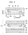
Fig. 3 is a schematic diagram of the solar cell
module of Example 1;
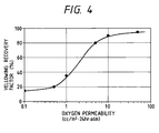
Fig. 4 is a graph showing the relationship between
oxygen permeability and yellowing recovery factor;
Fig. 5A, Fig. 5B, and Fig. 5C are views each
showing an example of building materials in the present
invention; and
Fig. 6 is a view showing an air circulation system
according to the present invention.
DESCRIPTION OF THE PREFERRED EMBODIMENTS
Fig. 1A is a view showing the schematic structure
of a solar cell module according to the present
invention. Reference numeral 101 designates a
photovoltaic element, the light-incidence-side surface
of which is covered by a surface covering member
comprised of at least a transparent surface sealant
resin layer 102 and a transparent surface protecting
film 103 located on the outermost surface side.
Numeral 104 denotes a back sealant resin layer, 105 a
back covering film, and 106 a nonwoven fabric of glass
fiber. Light from the outside is incident to the
outermost surface protecting film 103 to reach the
photovoltaic element 101 and electromotive force
generated is taken out through output terminals (not
illustrated). Fig. 1B shows an example having a module
backing 107 on the back surface of the solar cell
module of Fig. 1A. In Figs. 1A and 1B numeral 108
denotes a transparent, rigid, organic resin thin film
layer provided on the light incidence side of the
photovoltaic element 101.
(Surface protecting film 103)
Since the surface protecting film 103 employed in
the present invention is located as the outermost layer
of solar cell module, it needs to have the performance
for securing long-term reliability in outdoor exposure
of solar cell module, including the weathering
resistance, pollution resistance, and mechanical
strength.
The oxygen permeability of the surface protecting
film 103 needs to be not less than 1 cc/m2·24 hr·atm and
not more than 50 cc/m2·24 hr·atm at 25°C/90%RH and,
preferably, not less than 10 cc/m2·24 hr·atm and not
more than 50 cc/m2·24hr·atm.
Fig. 4 is a graph to show the relation between
oxygen permeability at 25°C/90%RH of the surface
protecting film and yellowing recovery factor of the
surface covering member. The relation between oxygen
permeability and yellowing recovery factor was obtained
as follows. A lamination was formed on slide glass in
such a structure that the outermost surface was an
organic resin film as the surface protecting film and
that an EVA resin containing the nonwoven fabric of
glass fiber was sealed between the slide glass and the
organic resin film. The EVA resin containing glass
fibers corresponds the surface sealant resin layer in
the solar cell module of the present invention. This
lamination was subjected to a thermal degrading test at
150°C and for 15 hours. The thermal degrading test
showed that yellowing of the sealant resin layer took
place to greatly decrease the optical transmittance and
that the decrease was equivalent to an almost 10% drop
in output of solar cell module. Then it was exposed to
ultraviolet rays under the output of 100 mW/cm2 in the
wavelength range of 300 to 400 nm by use of a metal
halide lamp. The yellowing recovery factor is defined
as a relative value when the optical transmittance (at
wavelength 400 nm) immediately after the thermal
degrading test is determined to be 0 and when the
transmittance (at wavelength 400 nm) immediately after
fabrication of the lamination is determined to be 100%.
It is clear from Fig. 4 that considerable recovery
from yellowing is recognized if the oxygen permeability
of surface protecting film is at least 1 cc/m2·24 hr·atm
and that recovery is almost perfectly made to the
initial transmittance if the oxygen permeability is 10
cc/m2·24 hr·atm or more.
Namely, supply of more oxygen to the sealant resin
facilitates the recovery from yellowing during the
exposure to ultraviolet light. A mechanism of this
recovery is conceivably such that conjugated double
bonds in main chains of polymer, which are the cause of
yellowing, are reduced by oxygen radicals generated by
ultraviolet irradiation over oxygen molecules having
diffused into the sealant resin layer.
Under actual outdoor use circumstances the
yellowing by heat and the yellowing dissolving action
with ultraviolet light plus oxygen are so-called
competitive reactions simultaneously taking place.
Even under such circumstances the yellowing can be
suppressed by supply of oxygen.
On the other hand, the sealant resin layer is
normally crosslinked by radicals produced by thermal
decomposition of an organic peroxide. A small amount
of the organic peroxide usually remains in the sealant
resin layer without being decomposed completely. Since
the organic peroxide has the action to promote the
yellowing of sealant resin layer, the remaining amount
thereof after crosslinking of sealant resin should be
preferably controlled as small as possible. Increasing
the oxygen permeability of surface protecting film
makes possible volatilization of the remaining organic
peroxide through the surface protecting film and thus
results in further enhancing the yellowing suppressing
effect.
However, the permeability of water vapor also
increases with increase in the oxygen permeability.
Intrusion of water vapor into the sealant resin layer
would result in lowering adhesive force of the sealant
resin layer to the other material and causing peeling
of the surface covering member. It also causes
degradation of electrical insulation of the surface
covering member and degradation of performance of
photovoltaic element due to water. Accordingly, the
oxygen permeability of the surface protecting film
needs to be not more than 50 cc/m2·24 hr·atm. More
specifically, the water vapor permeability of the
surface protecting film is more preferably 20 g/m2·24 hr
or less at 40°C/90%RH. The lower limit of water vapor
permeability of the surface protecting film is more
preferably 1.0 g/m2·24 hr at 40°C/90%RH.
Materials suitably used for the surface protecting
film 103 are, for example, fluoride polymers and
acrylic resins. Among them, the fluoride polymers are
favorably used, because they are excellent in the
weathering resistance and pollution resistance.
Specific examples include polyvinylidene fluoride
resins, polyvinyl fluoride resins, and
tetrafluoroethylene-ethylene copolymers. The
polyvinylidene fluoride resins are excellent in terms
of the weathering resistance, while the
tetrafluoroethylene-ethylene copolymers are excellent
in terms of compatibility of the weathering resistance
and mechanical strength, and transparency.
The surface protecting film 103 needs to have some
thickness for securing the mechanical strength, but too
great thicknesses are not preferred from the viewpoint
of cost. Specifically, the thickness is preferably 20-200
µm and more preferably 30-100 µm.
For improving adhesion with the surface sealant
resin layer 102, one surface of the surface protecting
film 103 is preferably treated by a surface treatment
such as the corona treatment, plasma treatment, ozone
treatment, UV irradiation, electron beam irradiation,
or flame treatment. Among them, the corona discharge
treatment is preferably used, because its treatment
rate is large and it can increase the adhesive force
greatly by a relatively simple device.
(Surface sealant resin layer 102)
The surface sealant resin layer 102 is necessary
for covering unevenness of photovoltaic element 101
with a resin, for protecting the photovoltaic element
101 from severe external circumstances such as
temperature change, humidity, and impact, and for
securing adhesion between the surface protecting film
103 and the photovoltaic element 101. Therefore, it
needs to be excellent in the weathering resistance,
adhesion, filling property, heat resistance, low
temperature resistance, and impact resistance.
Resins to meet these requirements include, for
example, polyolefin based resins such as ethylene-vinyl
acetate copolymers (EVA), ethylene-methylacrylate
copolymers (EMA), ethylene-ethylacrylate copolymers
(EEA), and polyvinyl butyral resins, urethane resins,
silicone resins, and fluororesins. Among them, EVA is
preferably used, because it has well-balanced physical
properties for use of solar cell.
The surface sealant resin layer is preferably
crosslinked in order to enhance the heat resistance and
the crosslinking is more preferably controlled so as to
achieve the gel percentage of 70 wt% or more.
Particularly, in the case of EVA, it is preferably
crosslinked with the organic peroxide, which can
effectively prevent deformation or creep under use at
high temperatures.
The crosslinking with the organic peroxide is made
in such a way that free radicals produced from the
organic peroxide draw hydrogen and halogen atoms in the
resin to form C-C bonds. The known methods for
activating the organic peroxide include thermal
decomposition, redox decomposition, and ion
decomposition. In general, the thermal decomposition
method is favorably adopted. Specific examples of the
organic peroxide include, for example, hydroperoxide,
dialkyl (allyl) peroxide, diacyl peroxide, peroxy
ketal, peroxy ester, peroxy carbonate, ketone peroxide,
and so on. An amount of the organic peroxide added is
preferably 0.5 to 5 parts by weight relative to 100
parts by weight of the surface sealant resin.
The resins used for the surface sealant resin
layer 102 are those excellent in the weathering
resistance, but an ultraviolet absorbing agent may also
be added in order to further enhance the weathering
resistance or in order to protect the layer located
below the surface sealant resin layer. The ultraviolet
absorbing agent can be selected from known compounds
and is selected preferably from low-volatile
ultraviolet absorbing agents in consideration of use
environments of solar cell module. Specific examples
of such agents are various organic compounds including
salicylic acid based compounds, benzophenone based
compounds, benzotriazole based compounds, and
cyanoacrylate based compounds.
If a light stabilizer is also added together with
the ultraviolet absorbing agent, the surface sealant
resin layer 102 will become stabler to light. Typical
examples of the light stabilizer are hindered amine
based light stabilizers. The hindered amine based
light stabilizers do not absorb the ultraviolet light,
different from the ultraviolet absorbing agent, but
they demonstrate a great synergistic effect when used
with the ultraviolet absorbing agent. There are, of
course, other compounds functioning as a light
stabilizer than the hindered amine based stabilizers,
but colored stabilizers are not preferred for the
surface sealant resin layer 102 of the present
invention. Contents of the above ultraviolet absorbing
agent and light stabilizer added are preferably 0.1-1.0
wt% and 0.05-1.0 wt%, respectively, to the surface
sealant resin.
Further, a thermal oxidation inhibitor may be
added for improving the thermal resistance and thermal
processability. The thermal oxidation inhibitor may be
selected, for example, from monophenol based compounds,
bisphenol based compounds, polymer type phenol based
compounds, sulfur based compounds, and phosphoric acid
based compounds. A content of the thermal oxidation
inhibitor added is preferably 0.05-1.0 wt% to the
surface sealant resin.
A silane coupling agent or an organic titanate
compound can be added to the surface sealant resin, for
further enhancing adhesion between the glass fibers 106
described below and the surface sealant resin. It also
presents an effect to enhance the adhesive force
between the surface sealant resin layer 102 and the
photovoltaic element 101 or the surface protecting film
103. An amount of the addition is preferably 0.1-3
parts by weight and more preferably 0.25-1 part by
weight to 100 parts by weight of the surface sealant
resin.
On the other hand, the surface sealant resin layer
102 needs to be transparent in order to control
decrease in quantity of light reaching the photovoltaic
element 101 to as low level as possible. Specifically,
the optical transmittance thereof is preferably 80% or
more and more preferably 90% or more in the visible
light wavelength region of 400 nm inclusive to 800 nm
inclusive. For facilitating incidence of light from
the atmosphere, the refractive index of the surface
sealant resin layer 102 at 25°C is preferably between
1.1 and 2.0 and more preferably between 1.1 and 1.6.
EVA sheets for solar cell in a sheet form of EVA
containing the above additives are commercially
available. Examples of such commercially available EVA
sheets are solar EVA from Hisheet Kogyo Kabushiki
Kaisha, EVASAFE WG series from BRIDGESTONE CORP.,
PHOTOCAP from SPRINGBORN LABORATORIES INC., and so on.
One selected from these is put between the photovoltaic
element 101 and the surface member such as the surface
protecting film 103 and they are pressed under heat,
whereby the solar cell module can be fabricated
readily.
(Glass fiber nonwoven fabric 106)
The surface sealant resin layer 102 preferably
contains the glass fiber nonwoven fabric 106. The
glass fiber nonwoven fabric 106 has a function to help
degassing from spaces in the solar cell module
lamination in a vacuuming step in a vacuum lamination
process and a function to prevent the surface sealant
resin from flowing to the module edges to thin the
surface sealant resin layer 102, as being impregnated
in the surface sealant resin of EVA or the like melted
in a heating step. Further, since the glass fiber
nonwoven fabric 106 is impregnated in the surface
sealant resin, it also functions as a reinforcing
material of the surface sealant resin layer 102,
thereby presenting an effect to make it harder for a
flaw in the surface to propagate to the photovoltaic
element 101.
The glass fiber nonwoven fabric 106 is obtained by
binding glass fibers with a binder resin. The binder
resin may be selected, for example, from acrylic
resins, urethane resins, polyvinyl alcohol resins,
polyester resins, and EVA resins, and it is selected
preferably from the acrylic resins in terms of the heat
resistance.
A rate of the glass fiber nonwoven fabric 106 to
the surface sealant resin is preferably 1-30 parts by
weight and more preferably between 5-20 parts by weight
to 100 parts by weight of the surface sealant resin.
If the rate is below one part by weight, there is such
a tendency that the surface covering member is unlikely
to have sufficient scratch resistance. If the rate is
over 30 parts by weight, an amount of glass fibers will
be excessive to the surface sealant resin, which will
cause failure of appearance, because the glass fiber
nonwoven fabric is not impregnated well in the surface
sealant resin in the module lamination step or which
will readily raise a problem of poor appearance or
separation of glass fibers from the surface sealant
resin layer 102 in long-term outdoor exposure.
The surface of the surface covering member is
often provided with unevenness in consideration of
decrease of reflected light, suppression of occurrence
of wrinkle upon lamination, design, and so on. The
maximum level difference between adjacent depressed and
projected portions of the unevenness is preferably
between 5 µm inclusive and 100 µm inclusive. If the
maximum level difference is below 5 µm, there is such a
tendency that the effect of provision of the unevenness
cannot be demonstrated well. If the maximum level
difference is over 100 µm, the surface sealant resin
layer 102 will be locally thin in depressed portions
where the amount of glass fibers tends to be excessive
to the surface sealant resin. With too deep
unevenness, thus, glass fibers tend to be separated
readily from the surface sealant resin layer 102 in the
depressed portions, thereby affecting the weathering
resistance of the surface covering member. This
unevenness may be formed during a cover forming step or
may be formed by a method of pressing or the like after
formation of cover.
(Back sealant resin layer 104)
The back sealant resin layer 104 is given for
adhesion between the photovoltaic element 101 and the
back covering film 105. Preferred materials for the
back sealant resin layer 104 are those capable of
securing sufficient adhesion to the substrate,
excellent in long-term durability, resistant to thermal
expansion and thermal contraction, and flexible.
Preferably used materials are, for example, resins
including hot melt materials such as EVA, EEA, or
polyvinyl butyral, and epoxy adhesives having
flexibility, and two sided adhesive tapes. It is a
matter of course that the back sealant resin layer 104
can also be made of the same material as the surface
sealant resin layer 102, which is normally the case in
many applications.
(Back covering film 105)
The back covering film 105 is necessary for
maintaining electrical insulation between the substrate
of the photovoltaic element 101 and the outside.
Preferred materials are those capable of securing
sufficient electrical insulation to the substrate,
excellent in long-term durability, resistant to thermal
expansion and thermal contraction, and flexible.
Suitably applicable films are, for example, films of
nylons and polyethylene terephthalate. It is also
possible to use a lamination film in which the back
sealant resin 104 and back covering film 105 described
above are preliminarily stacked together.
(Module backing 107)
The module backing may be adhered to the outside
of back covering film 105 in order to increase the
mechanical strength of solar cell module or in order to
prevent distortion or warpage due to temperature
change. The backing 107 is preferably selected, for
example, from steel sheets, plastic sheets, FRP (glass
fiber reinforced plastics) sheets, or flexible resin
sheets.
When a steel sheet is used as the module backing
107, a building material such as a wall material or a
roofing material incorporating the solar cell can be
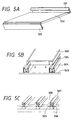
made by folding it. Figs. 5A-5C show examples of
roofing materials according to the present invention.
Fig. 5A shows a roofing material of a type where ridge-side
connecting portion 501 and eaves-side connecting
portion 502 are semi-jointed with each other. Fig. 5B
shows a roofing material of a type where engaging
portions thereof 505 are fitted in fixing members 504
fixed on sheathing roof board 503. Fig. 5C shows
roofing materials connecting parts of which are covered
by caps 507 after adjacent roofing materials are
connected at connecting parts thereof 506 by the fixing
members. A photovoltaic element 500 is provided in a
light receiving surface of each roofing material in the
examples shown.
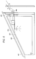
An air circulation system can be constructed as
shown in Fig. 6 by use of these roofing materials.
Fig. 6 shows an example of application of the
aforementioned combination solar cell and roofing
member to the air circulation system of house. Arrows
in the drawing indicate flows of air and the external
air taken in through eave part 601 is guided in space
604 between roofing materials 602 and roof underlayment
603 to be taken through ridge part 605 into the house.
A fan F is provided midway of air flow path to
circulate the air. In the cold season the air warmed
up in the space 604 is taken into the room and in the
hot season the air is discharged through exhaust port
606 to the outside, thereby enhancing heat insulation
performance of roof. A heat accumulating device may be
provided below the floor.
Power generated in the combination solar cell and
roofing members 602 is led through the ridge into the
house and then to inverter I, thus constituting a solar
electric power generation system. The output from the
solar electric power generation system may be consumed
at load L such as a lamp or may be sent to the
commercial electrical power system E.
(Photovoltaic element 101)
The photovoltaic element 101 employed in the
present invention can be made of a monocrystalline,
polycrystalline, microcrystalline, or amorphous
semiconductor. The material is selected from silicon
based or compound based semiconductor materials. A
typical example of the photovoltaic element 101
according to the present invention is a one obtained by
forming a nonmonocrystalline semiconductor photoactive
layer and a transparent, conductive layer on a
substrate.
Figs. 2A and 2B are views to show the schematic
structure of the example. Fig. 2A is a cross-sectional
view and Fig. 2B is a top plan view of the light
receiving surface side. In Figs. 2A and 2B, reference
numeral 201 designates a substrate, 202 a back
reflecting layer, 203 a semiconductor photoactive
layer, 204 a transparent, conductive layer, 205 a
collector electrode pattern, and 206 output terminals.
The substrate 201 functions as a substrate of
photovoltaic element and also functions as a lower
electrode. The substrate 201 may be made of a material
selected, for example, from silicon, tantalum,
molybdenum, tungsten, stainless steel, aluminum,
copper, titanium, carbon sheet, galvanized sheet iron,
or resin films or ceramics on which a conductive layer
of metal or metallic oxide is formed.
A metal layer, or a metallic oxide layer, or a
combination of the metal layer and metallic oxide layer
may be formed as a back reflecting layer 202 on the
substrate 201. The metal layer is, for example, of Ti,
Cr, Mo, W, Al, Ag, or Ni and the metallic oxide layer
is, for example, of ZnO, TiO2, or SnO2. The back
reflecting layer 202 can be made by a method selected
from the resistance heating vapor deposition method,
the electron beam vapor deposition method, the
sputtering method, and so on.
The semiconductor photoactive layer 203 is a
section for undergoing photoelectric conversion.
Specific examples of materials for the semiconductor
photoactive layer 203 include nonmonocrystalline
semiconductors such as pn junction type polycrystalline
silicon materials or pin junction type amorphous
silicon materials, and compound semiconductors
including CuInSe2, CuInS2, GaAs, CdS/Cu2S, CdS/CdTe,
CdS/InP, and CdTe/Cu2Te. Among them, the
nonmonocrystalline semiconductors are preferably used
and amorphous silicon is more preferred.
The semiconductor photoactive layer 203 may be
made by sheeting of molten silicon or by a heat
treatment of amorphous silicon in the case of
polycrystalline silicon; or by a plasma enhanced CVD
method using silane gas or the like as a raw material
in the case of amorphous silicon; or by ion plating,
ion beam deposition, vacuum vapor deposition,
sputtering, or electrodeposition in the case of the
compound semiconductors.
The transparent, conductive layer 204 serves as an
upper electrode of the photovoltaic element. The
transparent, conductive layer 204 may be made of a
material selected, for example, from In2O3, SnO2, In2O3-SnO2
(ITO), ZnO, TiO2, Cd2SnO4, and crystalline
semiconductors doped with a high concentration of
impurities. A method for forming the transparent,
conductive layer 204 may be selected from the
resistance heating vapor deposition, sputtering,
spraying, CVD, and impurity diffusion method.
The collector electrode 205 (grid) of a grating
pattern may be provided on the transparent, conductive
layer 204, for efficiently collecting electric
currents. Specific materials for the collector
electrode 205 are, for example, Ti, Cr, Mo, W, Al, Ag,
Ni, Cu, Sn, or conductive pastes including a silver
paste. The conductive pastes usually used are those
wherein fine powder of silver, gold, copper, nickel, or
carbon is dispersed in a binder polymer. The binder
polymer is selected, for example, from polyester,
epoxy, acrylic, alkyd, polyvinyl acetate, rubber,
urethane, and phenol resins.
A method for making the collector electrode 205
may be selected from sputtering with a mask pattern,
resistance heating, the CVD process, a method for first
evaporating a metal film over the entire surface and
thereafter patterning it by removing unnecessary
portions by etching, a method for directly forming the
grid electrode pattern by photo-CVD, a method for first
forming a mask of a negative pattern of the grid
electrode pattern and then performing plating thereon,
a method for printing a conductive paste, and a method
for bonding metal wires with a conductive paste.
Finally, the output terminals 206 are attached to
the substrate 201 and to the collector electrode 205,
for taking out the electromotive force. Metal member
206b of a belt shape, for example, of copper is joined
with the substrate 201 by soldering 208 or is
electrically connected therewith by spot welding with
laser. Metal member 206a of a belt shape, for example,
of copper is electrically connected with the collector
electrode 205 by conductive paste 207 or by soldering.
Photovoltaic elements produced by the above
techniques are connected in series or in parallel,
depending upon desired voltage or electric current.
Another arrangement may be such that photovoltaic
elements are integrated on an insulated substrate to
achieve desired voltage or current.
(Transparent, rigid, organic resin thin film layer 108)
Further, the transparent, rigid, organic resin
thin film layer 108 may be provided on the light
incidence side of the photovoltaic element in order to
present humidity resistance or scratch resistance.
Examples of materials for the layer 107 are acrylic
resins, silicone resins, acryl silicone resins,
polyalkoxy silane resins, fluororesins, polyester
resins, urethane resins, epoxy resins, alkyd resins,
polysilazane resins, and so on. Materials preferred in
view of weathering resistance are the acrylic resins,
silicone resins, acryl silicone resins, and
fluororesin. More preferred materials are resins
mainly containing the acrylic resin or the acryl
silicone resin. These resins are preferably
crosslinked to enhance heat resistance in consideration
of use of solar cell module at high temperatures. A
method for crosslinking is selected from normal methods
using the organic peroxide or isocyanate.
(Method for fabrication of solar cell module)
A normal method for covering the light receiving
surface of photovoltaic element 101 by the surface
sealant resin layer 102, the surface protecting film
103, and the glass fiber nonwoven fabric 106 is a
method for forming a sheet of surface sealant resin and
heat-pressing it on the photovoltaic element 101
together with the surface protecting film 103 and glass
fiber nonwoven fabric 106. Namely, the solar cell
module can be made by heat-pressing a stack in which
the surface sealant resin sheet and glass fiber
nonwoven fabric 106 are interposed between the
photovoltaic element 101 and the surface protecting
film 103. At this time, if a member having an uneven
shape is placed outside of the surface protecting film
103 and is arranged to be urged against the surface
protecting film 103 upon pressing, unevenness can be
made readily in the surface of surface covering member.
Heating temperature and heating time upon pressing
may be determined as occasion may demand. When the
surface sealant resin layer is of a crosslinked resin,
they can be determined by the temperature and time for
allowing sufficient progress of crosslinking reaction,
specifically, by thermal decomposition temperature
characteristics of the organic peroxide. In general,
heat pressing is completed by the temperature and time
for permitting progress of 90% of thermal decomposition
and, more preferably, progress of 95% or more of
thermal decomposition.
As for the back surface, covering may be made
using the back covering film 105 and back sealant resin
by the same method. Since the surface sealant resin
and the back sealant resin are normally the same
material, the back covering step can be carried out at
the same time as the above step. For example, the
solar cell module can be made by stacking the surface
protecting film 103/the surface sealant resin sheet/the
glass fiber nonwoven fabric 106/the photovoltaic
element 101/the back sealant resin sheet/the back
covering film 105 in this order to form a solar cell
module laminate and heat-pressing it. The surface
sealant resin sheet is melted by heating to take the
glass fibers 106 into the inside thereof, thus becoming
the surface sealant resin 102. The back sealant resin
sheet is also melted by heating to become the back
sealant resin 104 covering the back surface of
photovoltaic element 101. A method for heat pressing
may be selected from a variety of conventionally known
methods such as vacuum lamination or roll lamination.
The solar cell module of the present invention
preferably has the maximum use temperature of 70°C or
more. This permits us to expect an effect of recovery
from light degradation, particularly, of amorphous
semiconductor and also permits us to enjoy the maximum
yellowing suppressing effect of the surface sealant
resin layer purposed by the present invention.
(Examples)
The present invention will be described in further
detail with examples, but it is noted that the present
invention is by no means intended to be limited to the
examples and that the present invention can involve a
variety of modifications and changes within the scope
of the spirit thereof.
The following accelerated degrading tests were
conducted for checking the long-term reliability of
module.
(1) Light resistance
The solar cell modules were put in an ultraenergy
irradiation test machine (available from Suga Shikenki)
to be subjected to a due cycle test for repeating
exposure to ultraviolet light for five hours with a
metal halide lamp (exposure intensity: 100 mW/cm2 at 300
nm-400 nm, atmosphere: black panel temperature
70°C/humidity 70%RH) and dew condensation (temperature
30°C/humidity 96%RH) for one hour, and then change in
the appearance was observed after 2000 hours.
Observation results were indicated by ○ for no change
and a brief comment of condition for some change.
(2) Weathering resistance
The solar cell modules were put in a sunshine
weatherometer (available from Suga Shikenki) to be
subjected to an accelerated weathering test for
repeating 8-minute showers every two hours with
exposure to light (exposure intensity: 3 SUN,
atmosphere: black panel temperature 83°C/humidity
50%RH) with a xenon lamp, and change in the appearance
was observed after 5000 hours. Observation results
were indicated by ○ for no change and by a brief
comment of condition for some change.
(3) Humidity resistance
The solar cell modules were put in an
environmental test machine to be kept still under the
circumstances of temperature 85°C/humidity 85%RH for
1000 hours, and change in the appearance was observed.
Observation results were indicated by ○ for no change
and by a brief comment of condition for some change.
(Example 1)
[Photovoltaic element]
Amorphous silicon (a-Si) photovoltaic elements
having the structure shown in Figs. 2A and 2B were
fabricated in the following procedures.
An Al layer (5000 Å thick) and a ZnO layer (5000 Å
thick) were successively made as the back reflecting
layer 202 on the cleaned stainless steel substrate 201
by sputtering.
Then the tandem type a-Si semiconductor
photoactive layer 203 was made in the layer structure
of n-layer 150 Å thick/i-layer 4000 Å thick/p-layer 100
Å thick/n-layer 100 Å thick/i-layer 800 Å thick/p-layer
100 Å thick by making the n-type a-Si layers from
mixture gas of SiH4, PH3, and H2, the i-type a-Si layers
from mixture gas of SiH4 and H2, and the p-type
microcrystalline µc-Si layers from mixture gas of SiH4,
BF3, and H2 by the plasma enhanced CVD process.
Next, a thin film of In2O3 (700 Å thick) was made
as the transparent, conductive layer 204 by evaporating
In under an O2 atmosphere by the resistance heating
method.
Further, the grid electrode lines as the collector
electrode 205 were made by screen printing of silver
paste, a copper tab as the minus output terminal 206b
was attached to the substrate 201 with stainless
soldering 208, and a tape of tin foil as the plus
output terminal 206a was attached to the collector
electrode 205 with a conductive adhesive 207, thus
obtaining the photovoltaic element. The plus output
terminal 206a was routed through an insulator to the
back side and the output was arranged to be taken out
through holes of the back covering member described
below. A plurality of photovoltaic elements were made
in this way.
[Formation of module]
As shown in Fig. 3, the photovoltaic element 301
obtained as described above was covered by the
transparent, rigid, organic resin thin film layer 304.
The transparent, rigid, organic resin thin film layer
304 was made as follows. A solution was prepared by
adding 2.8 parts by weight of γ-metacryloxy
propyltrimetoxy silane (trade name: SH6040, available
from Toray Dow Corning Silicone Inc.) as a silane
coupling agent to 100 parts by weight of a coating
(trade name: Fine Hard N36-21F, resin solid content
30%, available from Showa Technocoat) in which an
acrylic resin, an inorganic polymer, and hexamethylene
diisocyanate blocked by ε-caprolactam were uniformly
dissolved or dispersed in an organic solvent. The
solution was applied by an airless spray to the light
receiving surface of photovoltaic element 301 and the
surface was heated at 200°C for ten minutes to
evaporate the solvent and to crosslink the resin, thus
making the transparent, rigid, organic resin thin film
layer 304.
The solar cell module lamination 310 was made by
stacking the photovoltaic element 301, a glass fiber
nonwoven fabric 309 (trade name: Glassper, basis weight
80 g/m2, available from Honshu Seishi), an EVA sheet as
the sealant resin layer 302 (trade name: PHOTOCAP,
thickness 460 µm, available from SPRINGBORN
LABORATORIES INC.), a non-oriented ETFE film having a
corona-discharge-treated surface as the surface
protecting film 303 (trade name: TEFZEL film, thickness
50 µm, available from DuPont Inc.), a nylon film as the
back covering film 305 (trade name: Dertec, thickness
63.5 µm, available from DuPont Inc.), and a galvanized
sheet ion as the module backing 306 (trade name: Taima
color GL, thickness 0.27 mm, available from Daido
Kohan) in the order of ETFE/EVA/glass fiber nonwoven
fabric/element/EVA/nylon/EVA/steel sheet.
Then a stainless mesh (40 × 40 meshes, diameter of
line 0.15 mm) was placed via a fluorocarbon film for
release (trade name: Teflon PFA film, thickness 50 µm,
available from DuPont Inc.) outside of the surface
protecting film 303, and the lamination was heat-pressed
at 150°C for 30 minutes while degassing under
pressure with a vacuum laminator, thereby obtaining the
solar cell module. The rate of glass fiber nonwoven
fabric was 8.7 parts by weight to 100 parts by weight
of the surface sealant resin in the surface covering
member of this solar cell module. On the other hand,
the unevenness having the maximum level difference of
30 µm was formed in the surface of surface covering
member by the mesh.
The EVA sheet used for the sealant resin layer 302
is the one popularly used as a sealant of solar cell,
in which 1.5 parts by weight of the organic peroxide as
a crosslinking agent, 0.3 part by weight of the
ultraviolet absorbing agent, 0.1 part by weight of the
light stabilizer, 0.2 part by weight of the thermal
oxidation inhibitor, and 0.25 part by weight of the
silane coupling agent are blended to 100 parts by
weight of the EVA resin (the content of vinyl acetate:
33%). The binder resin of the glass fiber nonwoven
fabric 309 is the acrylic resin.
The output terminal 307a was preliminarily routed
to the back surface of photovoltaic element 301,
whereby after the lamination, the output was able to be
taken out from the output terminals 307a and 307b
through terminal outlets 308a, 308b preliminarily
perforated in the module backing 306.
The oxygen permeability of the surface protecting
film 303 used herein was 15 cc/m2·24 hr·atm at
25°C/90%RH and the water vapor permeability thereof was
11.5 g/m2·24 hr at 40°C/90%RH.
The evaluation results are shown in Table 1. As
apparent from Table 1, the solar cell module obtained
in this example showed good results in the all
accelerated degrading tests.
(Comparative Example 1-1)
Instead of the ETFE film in Example 1, a PCTFE
(polychlorotrifluoroethylene) film (trade name: Neofron
CTFE, thickness 50 µm, available from Daikin Kogyo) was
used as the surface protecting film 303. The PCTFE
film is known as a resin having a small gas
permeability among the fluororesin films. The oxygen
permeability and water vapor permeability of the PCTFE
film used herein were measured. The oxygen
permeability thereof was 0.5 cc/m2·24 hr·atm at
25°C/90%RH and the water vapor permeability thereof was
0.3 g/m2·24 hr at 40°C/90%RH.
The evaluation results are shown in Table 1. As
shown in Table 1, yellowing of the surface sealant
resin layer appeared in the light resistance and
weathering resistance tests and the output of solar
cell module was lowered by the decrease of incident
light quantity caused thereby.
(Comparative Example 1-2)
In place of the ETFE film in Example 1, a white
sheet of tempered glass for solar cell (trade name:
Solatex, thickness 3.2 mm, available from AFG Inc.) was
used as the surface protecting material. Using an
aluminum laminate Tedlar film (available from Tokai
Almi Haku) instead of the sheet ion on the back
surface, the solar cell module lamination was made in
the stacking order of glass/EVA/glass fiber nonwoven
fabric/element/EVA/aluminum laminate Tedlar film. Then
this lamination was placed with the glass down in the
vacuum laminator and was heat-pressed at 150°C for 30
minutes while degassing under pressure, thereby
obtaining the solar cell module.
It is needless to mention that glass has the
oxygen permeability and the water vapor permeability of
zero. It is thus considered that there is no supply of
oxygen to the surface sealant resin layer and no
volatilization of remaining organic peroxide from the
surface sealant resin layer.
The evaluation results are shown in Table 1. As
shown in Table 1, yellowing of the surface sealant
resin layer appeared in the light resistance and
weathering resistance tests and the output of solar
cell module was lowered by the decrease of incident
light quantity caused thereby. The degree of decrease
was greater than in Comparative Example 1-1.
(Example 2)
The solar cell module was fabricated in the same
manner as in Example 1 except that the glass fiber
nonwoven fabric 309 in Example 1 was replaced by
another (trade name: Craneglass, basis weight 80 g/m2,
available from Crane and Co., Inc.) containing the
binder resin of polyvinyl alcohol.
The evaluation results are shown in Table 1. As
shown in Table 1, no change was recognized in the
appearance in the all tests and good results were
attained.
(Comparative Example 2)
The solar cell module was fabricated in the same
manner as in Comparative Example 1-2 except that the
glass fiber nonwoven fabric 309 in Comparative Example
1-2 was replaced by the one containing the binder resin
of polyvinyl alcohol (trade name: Craneglass, basis
weight 80 g/m2, available from Crane and Co., Inc.).
The evaluation results are shown in Table 1. As
shown in Table 1, great yellowing appeared in the
surface sealant resin layer. It is conceivably due to
influence of thermal oxidation of the polyvinyl alcohol
resin.
(Example 3)
An EEA resin (the content of ethylacrylate: 25%)
formed in a sheet form was used as the sealant resin
layer 302 in Example 1. Blended in this resin were 1.5
parts by weight of the organic peroxide as the
crosslinking agent, 0.3 part by weight of the
ultraviolet absorbing agent, 0.1 part by weight of the
light stabilizer, 0.2 part by weight of the thermal
oxidation inhibitor, 0.25 part by weight of the silane
coupling agent, and 3.0 parts by weight of triallyl
isocyanurate as the crosslinking agent. The solar cell
module was fabricated in the same manner as in Example
1 except for the above.
The evaluation results are shown in Table 1. No
change was recognized in the appearance in the all
tests and good results were shown as in Example 1.
(Comparative Example 3)
The EEA resin (the content of ethylacrylate: 25%)
formed in the sheet form was used as the sealant resin
layer 302 in Comparative Example 1-2. The solar cell
module was fabricated in the same manner as in
Comparative Example 1-2 except for the above.
The evaluation results are shown in Table 1.
Yellowing of the surface sealant resin layer was
recognized, though it was lighter than in the case of
the EVA resin used as the surface sealant resin layer.
(Comparative Example 4)
The thickness of the ETFE film in Example 1 was
changed to 12 µm. The solar cell module was fabricated
in the same manner as in Example 1 except for it.
The oxygen permeability and water vapor
permeability of the ETFE film as the surface protecting
film used herein were measured, which showed that the
oxygen permeability was 60 cc/m2·24 hr·atm at 25°C/90%RH
and the water vapor permeability was 43 g/m2·24 hr at
40°C/90%RH.
This module was subjected to the same accelerated
degrading tests as in Example 1. As shown in the
table, the surface film was peeled off from the sealant
resin in the humidity resistance test.
| | Light resistance | Weathering resistance | Humidity resistance |
| Example 1 | ○ | ○ | ○ |
| Example 2 | ○ | ○ | ○ |
| Example 3 | ○ | ○ | ○ |
| Comparative Example 1-1 | slight yellowing of surface cover | yellowing of surface cover | ○ |
| Comparative Example 1-2 | yellowing of surface cover | yellowing of surface cover | ○ |
| Comparative Example 2 | great yellowing of surface cover | great yellowing of surface cover | ○ |
| Comparative Example 3 | slight yellowing of surface cover | slight yellowing of surface cover | ○ |
| Comparative Example 4 | ○ | ○ | peeling of surface film |
A solar cell module is constructed in such an
arrangement that a photovoltaic element is covered by
at least a sealant resin and a surface protecting film,
wherein an oxygen permeability of the surface
protecting film is not less than 1 cc/m2·24 hr·atm and
not more than 50 cc/m2·24 hr·atm at 25°C/90%RH, thereby
providing the solar cell module with high reliability
free of deterioration of the sealant resin,
particularly free of yellowing, in long-term outdoor
exposure use.