EP0812068A2 - Differentielle Ausgangstreiberschaltung mit gemeinsamen Bezugspunkt - Google Patents
Differentielle Ausgangstreiberschaltung mit gemeinsamen Bezugspunkt Download PDFInfo
- Publication number
- EP0812068A2 EP0812068A2 EP97480025A EP97480025A EP0812068A2 EP 0812068 A2 EP0812068 A2 EP 0812068A2 EP 97480025 A EP97480025 A EP 97480025A EP 97480025 A EP97480025 A EP 97480025A EP 0812068 A2 EP0812068 A2 EP 0812068A2
- Authority
- EP
- European Patent Office
- Prior art keywords
- output
- signal
- transistors
- reference current
- signals
- Prior art date
- Legal status (The legal status is an assumption and is not a legal conclusion. Google has not performed a legal analysis and makes no representation as to the accuracy of the status listed.)
- Granted
Links
Images


Classifications
-
- H—ELECTRICITY
- H03—ELECTRONIC CIRCUITRY
- H03K—PULSE TECHNIQUE
- H03K19/00—Logic circuits, i.e. having at least two inputs acting on one output; Inverting circuits
- H03K19/0175—Coupling arrangements; Interface arrangements
- H03K19/017545—Coupling arrangements; Impedance matching circuits
-
- H—ELECTRICITY
- H03—ELECTRONIC CIRCUITRY
- H03K—PULSE TECHNIQUE
- H03K19/00—Logic circuits, i.e. having at least two inputs acting on one output; Inverting circuits
- H03K19/003—Modifications for increasing the reliability for protection
- H03K19/00369—Modifications for compensating variations of temperature, supply voltage or other physical parameters
Definitions
- the invention is generally related to differential output drivers for use in high speed applications.
- the invention is generally related to controlling operating parameters such as propagation delay of such output drivers to ensure reliable signal transmission in a networked environment.
- SCI Scaleable Coherent Interface
- LVDS Low-Voltage Differential Signal
- the LVDS specification relies on differential communication, where a pair of wires are used to transmit a digital signal. A logic one bit is represented by a higher voltage on one of the pair of wires, with a logic zero bit represented by a higher voltage on the other wire.
- Differential signal transmission systems offer high speed signal transmission with relatively low voltage swings and good noise rejection.
- Capacitance is often difficult to change in a transmission system due to transmission line lengths and other concerns. Consequently, to increase the speed possible in a transmission system, it is typical to either decrease the voltage swing, or increase the current. Tradeoffs often must be made, however, because reducing voltage swing makes the system more susceptible to noise, while increasing the current increases power dissipation. While differential signal transmission offers significant improvements over non-differential protocols, there is nonetheless a continuing need to increase the speed of such systems without sacrificing reliability or substantially increasing power dissipation.
- the common mode component i.e., the average DC voltage output level
- the common mode component of a transmission signal affects both the power dissipation and the noise rejection aspects of the system.
- Additional demands are placed on the hardware within differential as well as other signal transmission systems.
- process variations within an integrated circuit chip if the drivers are on the same chip or between multiple chips (if the drivers are on separate chips) may vary one or more operating parameters of the individual drivers, e.g., propagation delay, relative to one another such that the drivers, while designed to share identical characteristics, do not closely track one another.
- propagation delay e.g., propagation delay
- output drivers have been designed to receive reference voltages to stabilize the outputs of the drivers.
- the reference voltages are often susceptible to power supply variations, and may be affected by voltage drops that may occur in different chips or regions of chips.
- output drivers have been designed to rely on another reference signal such as a current or a threshold voltage of a bias transistor. While the use of a current or a threshold voltage as a reference may reduce the influence of power supply variations, it has been found that process variations within an output driver integrated circuit chip often cause mismatches between output drivers located in different areas of the chip.
- the invention addresses these and other problems associated with the prior art in providing in one aspect an apparatus with a plurality of output drivers coupled to a reference current generator such that each output driver receives a substantially identical copy of a reference current signal for controlling one or more operational parameters of the output driver.
- a reference current By using a reference current, the reference for each driver is, relative to every other driver, substantially insensitive to supply voltage variations, chip temperature variations, and process variations.
- the drivers are permitted to track one another in response to any variations or sensitivities that may nonetheless remain in the reference current.
- the outputs of the drivers are substantially aligned with one another.
- the multiple output drivers may be utilized to generate multiples clock signals that are aligned with one another.
- multiple signals sent to a common destination may be aligned with one another.
- signal transmission speed may often be increased due to reduced concerns as to signal-to-signal misalignment.
- data reliability is increased for any given transmission speed.
- multiple copies of the reference current signal are generated within the same region of an integrated circuit chip, thereby minimizing any process variations within the chip that might cause variances between the individual copies of the reference current signal. Consequently, a precisely controlled reference signal may be conducted to different output drivers, regardless of their location on the chip, such that process variations that may exist between individual drivers do not cause operational differences between the drivers.
- an apparatus which includes a reference current generator generating a reference current signal, the reference current generator outputting a plurality of copies of the reference current signal; and a plurality of output drivers, each output driver receiving a copy of the reference current signal to control an operating parameter of the output driver; whereby the plurality of output drivers collectively track one another in response to the reference current signal generated by the reference current generator.
- a signal transmission system comprising a plurality of nodes interconnected with one another to transmit signals therebetween.
- Each node in the system includes a signal generator for generating a plurality of output signals; a reference current generator for generating a reference current signal, the reference current generator outputting a plurality of copies of the reference current signal; and a plurality of output drivers, each output driver receiving an output signal from the signal generator and transmitting the same to another node in the signal transmission system, each output driver further receiving a copy of the reference current signal from the reference current generator to control an operating parameter of the output driver.
- the invention also addresses additional problems associated with the prior art in providing in another aspect a differential output driver having a differential pair of transistors that are coupled to a power signal (either ground or supply voltage) through a common mode resistor that controls the common mode component of the driver output independent of the voltage swing of the output. Greater design flexibility is obtained since the common mode component of the driver output can be optimized for speed, power dissipation, etc., without affecting the voltage swing. Moreover, smaller voltage swings may be possible through independent control of the common mode component, thereby increasing the speed of the driver without degrading noise rejection performance.
- the common mode resistor is coupled to ground to provide a ground bias for the output driver.
- the output of the driver is accordingly less dependent upon the operating voltage of the power supply. Consequently, a common driver design may be utilized for different operating voltages, and moreover, different communication devices within a signal transmission system may typically utilize different operating voltages without producing mismatches between devices in the system.
- a differential output driver that receives a pair of differential input signals and outputs a pair of differential output signals.
- the output driver is adapted to receive a pair of power signals, and the output driver includes a differential pair of first and second transistors coupled in parallel, the first and second transistors each receiving as input an input signal associated with one of the differential input signals and outputting an output signal associated with one of the differential output signals; and a common mode resistor, coupling the first and second transistors to one of the power signals; whereby the common mode resistor controls a common mode component of the pair of differential output signals independent of a voltage swing component of the pair of differential output signals.
- FIGURE 1 is a functional block diagram of a first preferred signal transmission system consistent with the principles of the invention, where a plurality of I/O device are provided with a common signal such as a clocking signal from a controller.
- FIGURE 2 is a functional block diagram of a second preferred signal transmission system consistent with the principles of the invention, where a plurality of networked nodes communicate with one another using multiple signals.
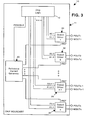
- FIGURE 3 is a functional block diagram of an integrated circuit chip consistent with the principles of the invention, for use in a node in either of the signal transmission systems of Figs. 1 and 2.
- FIGURE 4 is a schematic diagram of one of the output drivers from the chip of Figure 3.
- FIGURE 5 is a schematic diagram of an alternate output driver to that of Figure 4.
- FIGURE 6 is a schematic diagram of the reference current generator of Figure 3.
- FIGURE 7 is a functional diagram illustrating the preferred component layout of a portion of the reference current generator of Figure 6.
- Chip 11 generally includes chip logic, functionally illustrated as block 12, which generates a plurality of signals to be output from the chip.
- a plurality of output drivers 30 receive and output the signals as differential signals, and a reference current generator 20 generates a common reference current signal IREF to the output drivers such that the drivers track one another, in a manner which will be discussed in greater detail below.
- a signal transmission system 2 may include a plurality of I/O devices 4 coupled to a node 10 operating as a central controller for the system.
- System 2 may represent, for example, the clocking distribution for a remote I/O bus that couples a processor and memory subsystem with I/O subsystems in a computer system such as the AS/400 minicomputer from International Business Machines Corporation.
- the controller To synchronize the operation of the I/O devices, the controller provides a plurality of clock signals 3 to the devices. Therefore, to ensure adequate synchronization between the devices, the output drivers within node 10 preferably have the same propagation delay such that the clock signals passed to each device are substantially aligned with one another.
- a signal transmission system 5 may be a multinode network with nodes 6, 8 and 10 ⁇ coupled in a token ring configuration by a plurality of transmission lines 9. Each node outputs n signals to the next node in the ring.
- System 5 may represent, for example, a networked computer system which implements the IEEE Scaleable Coherent Interface (SCI) standard. It is desirable for reliability and speed concerns to align the n signals in each connection, and thus, the output drivers in each node preferably have the same propagation delay such that all signals passed between nodes are properly aligned with one another.
- SCI Scaleable Coherent Interface
- transmitting and receiving nodes may each represent a single integrated circuit chip, a circuit having a plurality of chips, or a fully functional controller, computer system, or other electronic device coupled through a network.
- the nodes may be coupled in any known point-to-point or bus network topology, e.g., fully connected, star, crossbar, mesh, and multidrop bus, among others. Therefore, the invention should not be limited to any particular network or node topology or components.
- Chip 11 is illustrated as a part of node 10 from Figure 1 representing a clock distribution chip for outputting multiple copies of a system clock signal to various devices coupled to node 10.
- chip 11 may be implemented in other applications, such as in node 10 ⁇ of the system of Figure 2.
- Chip 11 generally includes a plurality of output drivers, e.g., drivers 30 which provide a plurality (n) of differential output pairs, POUT1/MOUT1, POUT2/MOUT2, . . . , POUTn-1/MOUTn-1, and POUTn/MOUTn.
- the differential outputs preferably conform to the IEEE LVDS specifications of IEEE Standard 1596.3, although other output levels and specifications may also be used in the alternative.
- Each of the n output drivers 30 receives a pair of differential inputs, A0.1/A1.1, A0.2/A1.2, . . . , A0.n-1/A1.n-1, and A0.n/A1.n from a chip logic block (or signal generator) 12.
- Block 12 generally represents the primary logic circuitry of chip 11, which necessarily varies depending upon the function of chip 11.
- chip 11 may be a microprocessor or microcontroller, whereby block 12 represents the processing circuitry of the chip.
- chip 11 may be a dedicated driver chip, whereby block 12 may represent input buffer logic which receives inputs from another chip and outputs differential representations thereof.
- block 12 may represent a clock generator which generates a single differential clock signal at the desired frequency and outputs a plurality of copies thereof.
- a single differential clock signal may be output from block 12 and provided in parallel to the n output drivers 30.
- Drivers 30 also receive as input a copy of a reference current signal (IREF) from a reference current generator 20.
- the reference current signal functions both as a reference signal to control one or more operating parameters of the drivers, as well as an enable signal for turning the drivers on or off as a group.
- Reference current generator 20 receives a PENABLE signal from block 12 to enable/disable the outputs of the plurality of drivers 30.
- Figure 4 illustrates one of the output drivers 30 in greater detail, with its outputs POUT/MOUT (with the numerical designators thereof now removed) coupled to a receiver 52 of a node 4 (see Figure 1) through a twisted wire transmission line 50.
- a resistor R3 is shown terminating the transmission line, which is typically about 100 ⁇ consistent with the LVDS specification.
- Output driver 30 includes a differential pair 36 of transistors biased to ground through a resistor network 38.
- the driver is controlled with the reference current signal by a two stage current mirror having stages 32, 34.
- Inputs A0 and A1 of driver 30 first pass through a pair of level shifting transistors Q0 and Q1 operating in a linear mode, which drop the voltage of each input by an amount equal to V BE , the drop from the base to emitter of each transistor.
- Transistors Q0 and Q1 are preferably npn bipolar transistors, although n-type field effect (i.e., NFET or NMOS) transistors may be used in the alternative.
- Transistors Q0 and Q1 each have a gate terminal (the base) and first and second terminals (the collector and the emitter).
- the gate, first and second terminals thereof may represent herein the base, collector, and emitter (if a bipolar) or the gate, source and drain (if a field effect).
- the first and second terminals may refer herein to either the source or drain of a transistor.
- the first terminals of transistors Q0 and Q1 are coupled to the supply voltage, and the second terminals feed into the gate inputs of the differential pair 36 of first and second transistors T4 and T5.
- Transistors T4 and T5 act as switches to energize either POUT or MOUT depending upon input signals A0 and A1. If A0 is low and A1 is high, POUT goes low and MOUT goes high, and if A0 is high and A1 is low, POUT goes high and MOUT goes low.
- Transistors T4 and T5 are biased to ground through a resistor network 38 with first and second resistors R0 and R1 and a common mode resistor R2.
- the addition of common mode resistor R2 permits the common mode component of the output driver output to be controlled substantially independently from the voltage swing of the output, since current flow occurs through resistor R2 irrespective of whether transistor T4 or T5 is turned on.
- the resistors may typically be fabricated with highly controlled parameters using typical fabrication techniques, thus providing accurate control over the common mode component.
- resistor R2 is omitted (with resistors R0 and R1 terminating at ground), additional current, and thus power, is required to increase the common mode component of the output. Moreover, a greater voltage swing would accompany the additional current, thereby increasing the propagation delay through the driver.
- common mode resistor R2 reduces power dissipation and increases driver speed.
- driver output may be tailored to a swing and a common mode component which are suitable for receiver 52, in a much simpler manner.
- the same output driver design may be used with different supply voltages, and often the supply voltage of the receiver need not be matched with that of the output driver.
- a two stage current mirror with stages 32, 34 controls the current through transistors T4 and T5 with a reference transistor T7 coupling the first terminals of transistors T4 and T5 with the supply voltage V DD .
- the first stage 32 of the current mirror includes a transistor T0 with its second terminal coupled to ground and its gate and first terminals receiving the reference current signal IREF.
- a transistor T3 has its second terminal coupled to ground and the gate terminal receiving the reference current signal IREF.
- Transistor T3 preferably has a width to length ratio (W/L) that is three times that of transistor T0, thereby scaling the reference current signal by a factor of three at its first terminal.
- Second stage 34 includes transistor T6 and reference transistor T7.
- the gate terminals of transistors T6 and T7 and the second terminal of transistor T6 are coupled to the first terminal of transistor T3, while the first terminals of transistors T6 and T7 are coupled to the supply voltage V DD .
- the second terminal of transistor T7 is coupled to the first terminals of transistors T4 and T5.
- Reference transistor T7 preferably has a W/L that is ten times that of transistor T6, thereby further scaling the reference current signal by a factor of ten, for an overall scaling of thirty.
- the reference current signal is about 0.4 mA, and thus the current drawn through reference transistor T7 and output from the driver is about 12.0 mA.
- First stage 32 also includes a pair of transistors T1 and T2 which, similar to transistor T3, also receive the reference current signal at their gate terminals and are coupled to ground through their second terminals.
- the first terminals of transistors T1 and T2 are respectively coupled to the second terminals (emitters) of level shifting transistors Q0 and Q1.
- the W/L ⁇ s of transistors T1 and T2 are preferably about five times that of transistor T0, thus scaling the reference current signal by a factor of five (2.0 mA in the preferred embodiment).
- the voltage at the first terminals of level shifting transistors Q0 and Q1 is dominated by transistors Q0 and Q1.
- transistors T1 and T2 operate to control the current through, and thus the speed of, transistors Q0 and Q1.
- the reference current signal IREF controls the overall speed (i.e., the propagation delay or skew) of driver 30. Moreover, IREF also controls the output levels (voltage swing and common mode component) of the driver. Further, if no reference current signal is received, the output of the driver goes low. Consequently, through appropriate control of the scaling factors of the reference current and the selection of resistors R0-R2, the output characteristics of driver 30 are easily and reliably controlled.
- transistors T0, T1, T2 and T3 are preferably n-type field effect transistors (i.e., NMOS or NFET), while transistors T4, T5, T6 and T7 are p-type field effect transistors (i.e., PMOS or PFET).
- NMOS n-type field effect transistors
- transistors T4, T5, T6 and T7 are p-type field effect transistors (i.e., PMOS or PFET).
- the use of field effect transistors is preferred for speed considerations, although other types of transistors may be used in the alternative.
- driver 30 may be flipped, as illustrated by output driver 30 ⁇ of Figure 5, where corresponding components to those in driver 30 are designated by the same numbers, only primed.
- transistors T0 ⁇ , T1 ⁇ , T2 ⁇ and T3 ⁇ are p-type field effect transistors tied to the supply voltage
- transistors T4 ⁇ and T5 ⁇ are n-type field effect transistors biased to supply voltage through resistors R0 ⁇ , R1 ⁇ and R2 ⁇
- transistors T6 ⁇ and T7 ⁇ are n-type field effect transistors tied to ground.
- Level shifting transistors QO ⁇ and Q1 ⁇ are pnp bipolar transistors tied to ground, although p-type field effect transistors may be used in the alternative.
- Driver 30 ⁇ operates in substantially the same manner as driver 30, although this design has a greater dependency on the supply voltage and as a result may introduce some receiver matching problems.
- resistors R0 and R1 are 100 ⁇ resistors, while resistor R2 has a resistance of about 42 ⁇ . Coupled with the 12 mA current through reference transistor T7 and the 100 ⁇ termination on the transmission line, this results in a voltage swing of about 0.4 volts and a common mode component of about 1.1 volts.
- the current through transmission line 50 is about 4.0 mA and power dissipation is about 1.6 milliwatts (mW). With the length of the transmission line limited to 5 meters or less, the speed obtainable with driver 30 is about 500 MHz or greater.
- the supply voltage V DD provided to driver 30 is preferably between about 3.0 and 3.8 Volts. However, different supply voltages may be used consistent with the invention. For example, integrated circuit chips are commonly designed to operate at 5.0, 3.3 and 1.8 Volt operating voltages, among others. As the resistor network 38 couples the differential pair 36 of transistors to ground; however, the same driver design may be utilized for the preferred range of supply voltages.
- the reference current signal may be used to control a number of operating parameters of an output driver other than, or in addition to, the skew or output level of the driver.
- Other operating parameters which may be controlled at least in part by a reference current include output impedance, jitter, rise time, and symmetry, among others.
- each driver 30 in Figure 3 receives a reference current signal IREF generated by reference current generator 20, which is shown in greater detail in Figure 6.
- the primary purpose of generator 20 is to generate multiple precisely controlled copies of the reference current signal, although generator 20 also operates as an output enable circuit.
- the current mirror circuit includes a bank of m x n PFET output transistors, numbered TR0.0., TR0.1, . . . , TR0.n, TR1.1, . . . , TR1.n, . . . , TRm.0, TRm.1, . . . , TRm.n, which provide m x n copies of the current reference signal.
- Output enable module 24 receives an active high PENABLE enable signal from chip logic block 12 ( Figure 3) through a 1.0 K ⁇ resistor R10. The enable signal is then buffered through a pair of inverters 21, 22 with PFET transistors T10, T12 and NFET transistors T11 and T13, and passed to the gate terminal of a PFET transistor T16. A third inverter 23 with PFET transistor T14 and NFET transistor T15 also receives the buffered enable signal and provides a complementary (active low) enable signal to NFET transistor T20.
- PENABLE In operation, if PENABLE is low, node A is driven high and node B is pulled to ground, thereby shutting off transistors T17, T18, T19, T21 and T22 and disabling the bank of output transistors TR0.0 to TRm.n. If, however, PENABLE is high, transistors T16 and T20 are shut off in a high impedance state, and thus do not affect nodes A and B.
- PFET transistors T19 and T23 and NFET transistor T24 form startup circuit 25.
- node C is initially low, which turns on transistor T23 to charge node B. Once node B goes high, this pulls node A low, thereby turning on transistor T19. Then, when transistor T19 turns on, node C is pulled high, thereby shutting off transistor T23 and completing the startup process. In addition, at this point node A remains low, which then turns on output transistors TR0.0 to TRm.n.
- PFET transistors T17 and T18, NFET transistors T21 and T22, npn bipolar transistor Q10 and resistor R11 form supply independent current reference circuit 26.
- a capacitor C10 is also utilized for noise reduction and loop stability.
- Transistor Q10 has its base tied to its collector such that the transistor acts as a diode with a fixed voltage drop from the collector to the emitter.
- Transistors T17 and T18 form a current mirror, and are preferably the same size, so the currents through nodes D and E must be the same.
- transistors T21 and T22 are preferably the same size as one another, so the voltages at nodes D and E must also the same.
- Transistor Q10 coupled as a diode, sets the voltage at both nodes D and E to be the value of the voltage drop across the transistor -- a value which is independent of the supply voltage. With a known, supply independent voltage at node D, resistor R11 therefore controls the current through both nodes D and E, which is also substantially independent of the supply voltage.
- output transistors TR0.0 to TRm.n form current mirror circuit 27.
- Each output transistor forms a current mirror with transistor T17, and thus outputs a scaled copy of the current through nodes D and E.
- resistor R11 has a resistance of about 4.0 K ⁇ . With the fixed voltage drop of about 0.8 V across transistor Q10, the current through nodes D and E is about 0.2 mA. Further, each output transistor TR0.0 to TRm.n has a W/L ratio which is preferably twice that of transistor T17 such that the copy of the reference current signal output by each output transistor is twice that through nodes D and E. Consequently, each output transistor in the current mirror circuit of the preferred embodiment generates a reference current signal IREF of about 0.4 mA. It should be appreciated, however, that the size of each output transistor may be varied relative to transistor T17 to generate different reference current signals if desired. In addition, different sizes and values of components may be used to tailor the output of the reference current generator to any particular application.
- a preferred circuit topology is used to implement reference current generator 20 such that the copies of the reference current signal are carefully controlled.
- the output transistors TR0.0, . . ., TRm.n are all located proximate one another within the same region 28 of integrated circuit chip 11 to minimize any process variations between output transistors and thereby permit the output transistors to reliably track one another.
- transistors T17 and T18 are preferably located within the same region 28 as the output transistors, most preferably in the middle of the region, to further minimize process variations.
- the preferred embodiment of the invention has been found to be capable of generating multiple 0.4 mA copies of a reference current signal which deviate from one another by less than one percent.
- reference current generating circuits may be used, including those which reference the reference current to the supply voltage rather than ground.
- a supply independent reference current as well as to reference the generator to ground, as the design of the reference current generator becomes insensitive to the operating voltage of the power supply, thereby enabling the same design to be used for different supply or operating voltages (e.g., 5.0 V, 3.3 V or 1.8 V).
- different output driver circuits may be used in the alternative.
- the preferred output driver design has been found to be particularly well suited for use in many signal transmission systems due to its speed, reliability, and independent control of the common mode and voltage swing components of the differential output.
- the output driver and receiver do not necessarily have to utilize the same operating voltage.
- the same output driver design may be used with different operating voltages as with the preferred reference current generator.
Landscapes
- Engineering & Computer Science (AREA)
- Computer Hardware Design (AREA)
- Physics & Mathematics (AREA)
- Computing Systems (AREA)
- General Engineering & Computer Science (AREA)
- Mathematical Physics (AREA)
- Logic Circuits (AREA)
- Dc Digital Transmission (AREA)
- Small-Scale Networks (AREA)
Applications Claiming Priority (2)
| Application Number | Priority Date | Filing Date | Title |
|---|---|---|---|
| US08/659,293 US5767698A (en) | 1996-06-06 | 1996-06-06 | High speed differential output driver with common reference |
| US659293 | 1996-06-06 |
Publications (3)
| Publication Number | Publication Date |
|---|---|
| EP0812068A2 true EP0812068A2 (de) | 1997-12-10 |
| EP0812068A3 EP0812068A3 (de) | 1999-07-21 |
| EP0812068B1 EP0812068B1 (de) | 2004-09-15 |
Family
ID=24644846
Family Applications (1)
| Application Number | Title | Priority Date | Filing Date |
|---|---|---|---|
| EP97480025A Expired - Lifetime EP0812068B1 (de) | 1996-06-06 | 1997-05-23 | Differentielle Ausgangstreiberschaltung mit gemeinsamen Bezugspunkt |
Country Status (4)
| Country | Link |
|---|---|
| US (1) | US5767698A (de) |
| EP (1) | EP0812068B1 (de) |
| JP (1) | JPH1065515A (de) |
| DE (1) | DE69730649D1 (de) |
Cited By (1)
| Publication number | Priority date | Publication date | Assignee | Title |
|---|---|---|---|---|
| WO2003058903A1 (en) * | 2002-01-02 | 2003-07-17 | Intel Corporation | Low supply voltage differential signal driver |
Families Citing this family (28)
| Publication number | Priority date | Publication date | Assignee | Title |
|---|---|---|---|---|
| JPH10268995A (ja) * | 1997-03-25 | 1998-10-09 | Canon Inc | インターフェース制御方法及びその装置 |
| US5898297A (en) * | 1997-03-31 | 1999-04-27 | Sun Microsystems, Inc. | Differential high speed driver for low voltage operation |
| US5943635A (en) * | 1997-12-12 | 1999-08-24 | Scenix Semiconductor Inc. | System and method for programmable brown-out detection and differentiation |
| US5942922A (en) * | 1998-04-07 | 1999-08-24 | Credence Systems Corporation | Inhibitable, continuously-terminated differential drive circuit for an integrated circuit tester |
| JP4130709B2 (ja) * | 1998-06-23 | 2008-08-06 | 株式会社アドバンテスト | 半導体デバイス試験装置および信号出力装置 |
| JP2000252813A (ja) | 1999-02-24 | 2000-09-14 | Texas Instr Inc <Ti> | 低電圧差動信号方式受信機用出力バッファ |
| KR100360759B1 (ko) * | 1999-02-25 | 2002-11-18 | 가부시끼가이샤 도시바 | 집적회로장치 및 이를 이용한 액정표시장치 |
| JP3500322B2 (ja) * | 1999-04-09 | 2004-02-23 | シャープ株式会社 | 定電流駆動装置および定電流駆動半導体集積回路 |
| US6294937B1 (en) | 1999-05-25 | 2001-09-25 | Lsi Logic Corporation | Method and apparatus for self correcting parallel I/O circuitry |
| US6557066B1 (en) | 1999-05-25 | 2003-04-29 | Lsi Logic Corporation | Method and apparatus for data dependent, dual level output driver |
| US6130548A (en) * | 1999-07-09 | 2000-10-10 | Motorola Inc. | Signal converting receiver having constant hysteresis, and method therefor |
| US6292010B1 (en) | 2000-02-02 | 2001-09-18 | Teradyne, Inc. | Dynamic pin driver combining high voltage mode and high speed mode |
| JP3721069B2 (ja) | 2000-11-08 | 2005-11-30 | 富士通株式会社 | 入出力インタフェース回路、入出力インタフェース、および入出力インタフェース回路を有する半導体装置 |
| JP4735911B2 (ja) * | 2000-12-28 | 2011-07-27 | 日本電気株式会社 | 駆動回路及びこれを用いた定電流駆動装置 |
| US6469548B1 (en) | 2001-06-14 | 2002-10-22 | Cypress Semiconductor Corp. | Output buffer crossing point compensation |
| US6600347B2 (en) | 2001-10-10 | 2003-07-29 | International Business Machines Corporation | Dynamically producing an effective impedance of an output driver with a bounded variation during transitions thereby reducing jitter |
| US6788142B2 (en) | 2001-11-19 | 2004-09-07 | Broadcom Corporation | Wide common mode differential input amplifier and method |
| US6686772B2 (en) * | 2001-11-19 | 2004-02-03 | Broadcom Corporation | Voltage mode differential driver and method |
| US6960931B2 (en) * | 2002-10-30 | 2005-11-01 | International Business Machines Corporation | Low voltage differential signal driver circuit and method |
| US7034566B2 (en) * | 2004-02-12 | 2006-04-25 | International Business Machines Corporation | Method and circuit for increased noise immunity for clocking signals in high speed digital systems |
| EP1566723B1 (de) * | 2004-02-20 | 2007-11-21 | STMicroelectronics S.r.l. | Leistungsverwaltungseinheit für einen Flashspeicher mit einer gemeinsamen Regulierung mehrerer Ladungspumpen |
| US7342420B2 (en) * | 2004-09-24 | 2008-03-11 | Integrated Device Technology, Inc. | Low power output driver |
| JP4459099B2 (ja) * | 2005-03-18 | 2010-04-28 | キヤノン株式会社 | 固体撮像装置及びカメラ |
| JP2008092530A (ja) * | 2006-10-05 | 2008-04-17 | Nec Electronics Corp | 信号伝送回路 |
| US7940846B2 (en) * | 2007-01-08 | 2011-05-10 | International Business Machines Corporation | Test circuit for serial link receiver |
| JP5003346B2 (ja) | 2007-08-21 | 2012-08-15 | 日本電気株式会社 | 参照電圧生成回路及び参照電圧分配方法 |
| JP4949203B2 (ja) * | 2007-10-31 | 2012-06-06 | シャープ株式会社 | 基準電流回路、レシーバ回路、トランスミッタ回路およびシリアルインターフェイス回路 |
| JP6231291B2 (ja) * | 2013-03-28 | 2017-11-15 | ローム株式会社 | モータ駆動装置 |
Citations (3)
| Publication number | Priority date | Publication date | Assignee | Title |
|---|---|---|---|---|
| US4841175A (en) * | 1987-01-23 | 1989-06-20 | Siemens Aktiengesellschaft | ECL-compatible input/output circuits in CMOS technology |
| US5065055A (en) * | 1990-12-20 | 1991-11-12 | Sun Microsystems, Inc. | Method and apparatus for high-speed bi-CMOS differential amplifier with controlled output voltage swing |
| US5367201A (en) * | 1992-07-01 | 1994-11-22 | Telefonaktiebolaget L M Ericsson | Control circuit system for control of parameters in logic circuits or similar |
Family Cites Families (11)
| Publication number | Priority date | Publication date | Assignee | Title |
|---|---|---|---|---|
| JPS60113507A (ja) * | 1983-11-24 | 1985-06-20 | Nec Corp | トランジスタ回路 |
| NL8403693A (nl) * | 1984-12-05 | 1986-07-01 | Philips Nv | Adaptief electronisch buffersysteem. |
| US4999519A (en) * | 1987-12-04 | 1991-03-12 | Hitachi Vlsi Engineering Corporation | Semiconductor circuit with low power consumption having emitter-coupled logic or differential amplifier |
| US5144164A (en) * | 1988-03-18 | 1992-09-01 | Kabushiki Kaisha Toshiba | BiCMOS current switching circuit having a plurality of resistors of a specified value |
| US5021682A (en) * | 1989-05-11 | 1991-06-04 | National Semiconductor Corporation | Instantaneous power limiting circuit |
| GB2234872B (en) * | 1989-08-03 | 1994-04-06 | Plessey Co Plc | High speed CMOS differential interface circuits |
| US5216298A (en) * | 1989-12-14 | 1993-06-01 | Mitsubishi Denki Kabushiki Kaisha | ECL input buffer for BiCMOS |
| DE4224804C1 (de) * | 1992-07-27 | 1994-01-13 | Siemens Ag | Programmierbare logische Schaltungsanordnung |
| US5451898A (en) * | 1993-11-12 | 1995-09-19 | Rambus, Inc. | Bias circuit and differential amplifier having stabilized output swing |
| US5534803A (en) * | 1995-04-12 | 1996-07-09 | International Business Machines Corporation | Process insensitive off-chip driver |
| JP3547854B2 (ja) * | 1995-06-08 | 2004-07-28 | 株式会社ルネサステクノロジ | 駆動電流調整機能付きバッファ回路 |
-
1996
- 1996-06-06 US US08/659,293 patent/US5767698A/en not_active Expired - Lifetime
-
1997
- 1997-05-21 JP JP9130816A patent/JPH1065515A/ja active Pending
- 1997-05-23 EP EP97480025A patent/EP0812068B1/de not_active Expired - Lifetime
- 1997-05-23 DE DE69730649T patent/DE69730649D1/de not_active Expired - Lifetime
Patent Citations (3)
| Publication number | Priority date | Publication date | Assignee | Title |
|---|---|---|---|---|
| US4841175A (en) * | 1987-01-23 | 1989-06-20 | Siemens Aktiengesellschaft | ECL-compatible input/output circuits in CMOS technology |
| US5065055A (en) * | 1990-12-20 | 1991-11-12 | Sun Microsystems, Inc. | Method and apparatus for high-speed bi-CMOS differential amplifier with controlled output voltage swing |
| US5367201A (en) * | 1992-07-01 | 1994-11-22 | Telefonaktiebolaget L M Ericsson | Control circuit system for control of parameters in logic circuits or similar |
Non-Patent Citations (1)
| Title |
|---|
| "BIAS TECHNIQUE FOR ECL IN BICMOS TECHNOLOGY" IBM TECHNICAL DISCLOSURE BULLETIN, vol. 34, no. 3, 1 August 1991, pages 84-85, XP000210455 * |
Cited By (2)
| Publication number | Priority date | Publication date | Assignee | Title |
|---|---|---|---|---|
| WO2003058903A1 (en) * | 2002-01-02 | 2003-07-17 | Intel Corporation | Low supply voltage differential signal driver |
| US6617888B2 (en) | 2002-01-02 | 2003-09-09 | Intel Corporation | Low supply voltage differential signal driver |
Also Published As
| Publication number | Publication date |
|---|---|
| JPH1065515A (ja) | 1998-03-06 |
| EP0812068B1 (de) | 2004-09-15 |
| EP0812068A3 (de) | 1999-07-21 |
| DE69730649D1 (de) | 2004-10-21 |
| US5767698A (en) | 1998-06-16 |
Similar Documents
| Publication | Publication Date | Title |
|---|---|---|
| EP0812068B1 (de) | Differentielle Ausgangstreiberschaltung mit gemeinsamen Bezugspunkt | |
| KR100272671B1 (ko) | 데이터 트랜시버 및 그것을 갖는 버스 인터페이스 | |
| KR0179666B1 (ko) | 버스용 전기전류원회로 | |
| US5581556A (en) | Local area network system | |
| KR100356074B1 (ko) | 저 소비전력으로 2진 논리신호를 전송하는 인터페이스 회로 및 방법 | |
| US7113759B2 (en) | Controller area network transceiver having capacitive balancing circuit for improved receiver common-mode rejection | |
| JP2848500B2 (ja) | インタフェースシステム | |
| US5535241A (en) | Signal transmission system and method of operation | |
| US6597198B2 (en) | Current mode bidirectional port with data channel used for synchronization | |
| US5789937A (en) | Impedence self-adjusting driver circuit | |
| US20020191707A1 (en) | Data transmission circuit for universal serial bus system | |
| US6278312B1 (en) | Method and apparatus for generating a reference voltage signal derived from complementary signals | |
| JPH09502577A (ja) | Cmosbtl互換バス及び伝送線路ドライバ | |
| US6359465B1 (en) | CMOS small signal switchable adjustable impedence terminator network | |
| KR100342210B1 (ko) | 제조 공정, 공급 전압, 및 온도에 무관한 프로그램가능한 에지속도 제어 기능을 지니는 트랜시버 드라이버 | |
| US6373276B1 (en) | CMOS small signal switchable impedence and voltage adjustable terminator with hysteresis receiver network | |
| JP3159247B2 (ja) | 入力回路 | |
| EP0450453B1 (de) | BICMOS-Eingangsschaltkreis zur Erkennung von Signalen ausserhalb des ECL-Bereiches | |
| JP4359364B2 (ja) | インタフェース | |
| US20020089319A1 (en) | Current mirror circuit | |
| EP0821484B1 (de) | Hohen Spannungen widerstehende Ausgangsstufe | |
| JP2910679B2 (ja) | 半導体集積回路 | |
| WO1997009811A1 (en) | Low jitter low power single ended driver | |
| US6310490B1 (en) | CMOS small signal switchable, impedence and voltage adjustable terminator network and receiver integration | |
| US6693465B1 (en) | Open input sense for differential receiver |
Legal Events
| Date | Code | Title | Description |
|---|---|---|---|
| PUAI | Public reference made under article 153(3) epc to a published international application that has entered the european phase |
Free format text: ORIGINAL CODE: 0009012 |
|
| AK | Designated contracting states |
Kind code of ref document: A2 Designated state(s): DE FR GB |
|
| PUAL | Search report despatched |
Free format text: ORIGINAL CODE: 0009013 |
|
| AK | Designated contracting states |
Kind code of ref document: A3 Designated state(s): DE FR GB |
|
| 17P | Request for examination filed |
Effective date: 19991002 |
|
| AKX | Designation fees paid |
Free format text: DE FR GB |
|
| 17Q | First examination report despatched |
Effective date: 20020729 |
|
| GRAP | Despatch of communication of intention to grant a patent |
Free format text: ORIGINAL CODE: EPIDOSNIGR1 |
|
| GRAS | Grant fee paid |
Free format text: ORIGINAL CODE: EPIDOSNIGR3 |
|
| GRAA | (expected) grant |
Free format text: ORIGINAL CODE: 0009210 |
|
| AK | Designated contracting states |
Kind code of ref document: B1 Designated state(s): DE FR GB |
|
| PG25 | Lapsed in a contracting state [announced via postgrant information from national office to epo] |
Ref country code: FR Free format text: LAPSE BECAUSE OF FAILURE TO SUBMIT A TRANSLATION OF THE DESCRIPTION OR TO PAY THE FEE WITHIN THE PRESCRIBED TIME-LIMIT Effective date: 20040915 |
|
| REG | Reference to a national code |
Ref country code: GB Ref legal event code: FG4D |
|
| REF | Corresponds to: |
Ref document number: 69730649 Country of ref document: DE Date of ref document: 20041021 Kind code of ref document: P |
|
| PG25 | Lapsed in a contracting state [announced via postgrant information from national office to epo] |
Ref country code: DE Free format text: LAPSE BECAUSE OF FAILURE TO SUBMIT A TRANSLATION OF THE DESCRIPTION OR TO PAY THE FEE WITHIN THE PRESCRIBED TIME-LIMIT Effective date: 20041216 |
|
| PLBE | No opposition filed within time limit |
Free format text: ORIGINAL CODE: 0009261 |
|
| STAA | Information on the status of an ep patent application or granted ep patent |
Free format text: STATUS: NO OPPOSITION FILED WITHIN TIME LIMIT |
|
| 26N | No opposition filed |
Effective date: 20050616 |
|
| EN | Fr: translation not filed | ||
| REG | Reference to a national code |
Ref country code: GB Ref legal event code: 746 Effective date: 20090417 |
|
| PGFP | Annual fee paid to national office [announced via postgrant information from national office to epo] |
Ref country code: GB Payment date: 20160525 Year of fee payment: 20 |
|
| REG | Reference to a national code |
Ref country code: GB Ref legal event code: PE20 Expiry date: 20170522 |
|
| PG25 | Lapsed in a contracting state [announced via postgrant information from national office to epo] |
Ref country code: GB Free format text: LAPSE BECAUSE OF EXPIRATION OF PROTECTION Effective date: 20170522 |