EP0808918B1 - Appareillage de traitement par plasma et méthode de traitement - Google Patents
Appareillage de traitement par plasma et méthode de traitement Download PDFInfo
- Publication number
- EP0808918B1 EP0808918B1 EP97303434A EP97303434A EP0808918B1 EP 0808918 B1 EP0808918 B1 EP 0808918B1 EP 97303434 A EP97303434 A EP 97303434A EP 97303434 A EP97303434 A EP 97303434A EP 0808918 B1 EP0808918 B1 EP 0808918B1
- Authority
- EP
- European Patent Office
- Prior art keywords
- reaction vessel
- cathode electrodes
- plasma processing
- film
- matching circuit
- Prior art date
- Legal status (The legal status is an assumption and is not a legal conclusion. Google has not performed a legal analysis and makes no representation as to the accuracy of the status listed.)
- Expired - Lifetime
Links
- 238000012545 processing Methods 0.000 title claims description 58
- 238000003672 processing method Methods 0.000 title claims description 11
- 238000006243 chemical reaction Methods 0.000 claims description 131
- 239000000758 substrate Substances 0.000 claims description 104
- 238000000034 method Methods 0.000 claims description 34
- 239000003990 capacitor Substances 0.000 claims description 32
- 239000003989 dielectric material Substances 0.000 claims description 18
- 230000008569 process Effects 0.000 claims description 15
- 238000004544 sputter deposition Methods 0.000 claims description 7
- PNEYBMLMFCGWSK-UHFFFAOYSA-N Alumina Chemical compound [O-2].[O-2].[O-2].[Al+3].[Al+3] PNEYBMLMFCGWSK-UHFFFAOYSA-N 0.000 claims description 6
- 239000011521 glass Substances 0.000 claims description 6
- 238000005530 etching Methods 0.000 claims description 5
- 238000004380 ashing Methods 0.000 claims description 3
- 238000004519 manufacturing process Methods 0.000 claims description 2
- 229920001343 polytetrafluoroethylene Polymers 0.000 claims 2
- 238000005229 chemical vapour deposition Methods 0.000 claims 1
- 229910021417 amorphous silicon Inorganic materials 0.000 description 40
- 239000007789 gas Substances 0.000 description 37
- 230000005540 biological transmission Effects 0.000 description 34
- 238000009826 distribution Methods 0.000 description 21
- 238000005268 plasma chemical vapour deposition Methods 0.000 description 18
- 238000000151 deposition Methods 0.000 description 17
- 230000008021 deposition Effects 0.000 description 17
- NMFHJNAPXOMSRX-PUPDPRJKSA-N [(1r)-3-(3,4-dimethoxyphenyl)-1-[3-(2-morpholin-4-ylethoxy)phenyl]propyl] (2s)-1-[(2s)-2-(3,4,5-trimethoxyphenyl)butanoyl]piperidine-2-carboxylate Chemical compound C([C@@H](OC(=O)[C@@H]1CCCCN1C(=O)[C@@H](CC)C=1C=C(OC)C(OC)=C(OC)C=1)C=1C=C(OCCN2CCOCC2)C=CC=1)CC1=CC=C(OC)C(OC)=C1 NMFHJNAPXOMSRX-PUPDPRJKSA-N 0.000 description 15
- 239000000463 material Substances 0.000 description 15
- 230000015572 biosynthetic process Effects 0.000 description 13
- 238000002474 experimental method Methods 0.000 description 7
- 230000007246 mechanism Effects 0.000 description 7
- 230000002093 peripheral effect Effects 0.000 description 7
- BLRPTPMANUNPDV-UHFFFAOYSA-N Silane Chemical compound [SiH4] BLRPTPMANUNPDV-UHFFFAOYSA-N 0.000 description 6
- 230000000694 effects Effects 0.000 description 6
- 239000004065 semiconductor Substances 0.000 description 6
- 239000011810 insulating material Substances 0.000 description 5
- 238000012986 modification Methods 0.000 description 5
- 230000004048 modification Effects 0.000 description 5
- 239000000872 buffer Substances 0.000 description 4
- 230000005684 electric field Effects 0.000 description 4
- VNWKTOKETHGBQD-UHFFFAOYSA-N methane Chemical compound C VNWKTOKETHGBQD-UHFFFAOYSA-N 0.000 description 4
- 238000007599 discharging Methods 0.000 description 3
- OTMSDBZUPAUEDD-UHFFFAOYSA-N Ethane Chemical compound CC OTMSDBZUPAUEDD-UHFFFAOYSA-N 0.000 description 2
- 230000008859 change Effects 0.000 description 2
- 239000000470 constituent Substances 0.000 description 2
- 238000007796 conventional method Methods 0.000 description 2
- 230000003247 decreasing effect Effects 0.000 description 2
- PZPGRFITIJYNEJ-UHFFFAOYSA-N disilane Chemical compound [SiH3][SiH3] PZPGRFITIJYNEJ-UHFFFAOYSA-N 0.000 description 2
- 150000002500 ions Chemical class 0.000 description 2
- 239000002184 metal Substances 0.000 description 2
- 150000004767 nitrides Chemical class 0.000 description 2
- 229910000077 silane Inorganic materials 0.000 description 2
- 206010034972 Photosensitivity reaction Diseases 0.000 description 1
- VYPSYNLAJGMNEJ-UHFFFAOYSA-N Silicium dioxide Chemical compound O=[Si]=O VYPSYNLAJGMNEJ-UHFFFAOYSA-N 0.000 description 1
- 230000000052 comparative effect Effects 0.000 description 1
- 230000007423 decrease Effects 0.000 description 1
- 230000000593 degrading effect Effects 0.000 description 1
- 238000013461 design Methods 0.000 description 1
- 238000001312 dry etching Methods 0.000 description 1
- 230000006872 improvement Effects 0.000 description 1
- 230000003287 optical effect Effects 0.000 description 1
- 230000010355 oscillation Effects 0.000 description 1
- 230000036211 photosensitivity Effects 0.000 description 1
- 238000003786 synthesis reaction Methods 0.000 description 1
Images


Classifications
-
- H—ELECTRICITY
- H01—ELECTRIC ELEMENTS
- H01J—ELECTRIC DISCHARGE TUBES OR DISCHARGE LAMPS
- H01J37/00—Discharge tubes with provision for introducing objects or material to be exposed to the discharge, e.g. for the purpose of examination or processing thereof
- H01J37/32—Gas-filled discharge tubes
- H01J37/32009—Arrangements for generation of plasma specially adapted for examination or treatment of objects, e.g. plasma sources
- H01J37/32082—Radio frequency generated discharge
- H01J37/32091—Radio frequency generated discharge the radio frequency energy being capacitively coupled to the plasma
-
- C—CHEMISTRY; METALLURGY
- C23—COATING METALLIC MATERIAL; COATING MATERIAL WITH METALLIC MATERIAL; CHEMICAL SURFACE TREATMENT; DIFFUSION TREATMENT OF METALLIC MATERIAL; COATING BY VACUUM EVAPORATION, BY SPUTTERING, BY ION IMPLANTATION OR BY CHEMICAL VAPOUR DEPOSITION, IN GENERAL; INHIBITING CORROSION OF METALLIC MATERIAL OR INCRUSTATION IN GENERAL
- C23C—COATING METALLIC MATERIAL; COATING MATERIAL WITH METALLIC MATERIAL; SURFACE TREATMENT OF METALLIC MATERIAL BY DIFFUSION INTO THE SURFACE, BY CHEMICAL CONVERSION OR SUBSTITUTION; COATING BY VACUUM EVAPORATION, BY SPUTTERING, BY ION IMPLANTATION OR BY CHEMICAL VAPOUR DEPOSITION, IN GENERAL
- C23C14/00—Coating by vacuum evaporation, by sputtering or by ion implantation of the coating forming material
- C23C14/22—Coating by vacuum evaporation, by sputtering or by ion implantation of the coating forming material characterised by the process of coating
- C23C14/34—Sputtering
-
- C—CHEMISTRY; METALLURGY
- C23—COATING METALLIC MATERIAL; COATING MATERIAL WITH METALLIC MATERIAL; CHEMICAL SURFACE TREATMENT; DIFFUSION TREATMENT OF METALLIC MATERIAL; COATING BY VACUUM EVAPORATION, BY SPUTTERING, BY ION IMPLANTATION OR BY CHEMICAL VAPOUR DEPOSITION, IN GENERAL; INHIBITING CORROSION OF METALLIC MATERIAL OR INCRUSTATION IN GENERAL
- C23C—COATING METALLIC MATERIAL; COATING MATERIAL WITH METALLIC MATERIAL; SURFACE TREATMENT OF METALLIC MATERIAL BY DIFFUSION INTO THE SURFACE, BY CHEMICAL CONVERSION OR SUBSTITUTION; COATING BY VACUUM EVAPORATION, BY SPUTTERING, BY ION IMPLANTATION OR BY CHEMICAL VAPOUR DEPOSITION, IN GENERAL
- C23C16/00—Chemical coating by decomposition of gaseous compounds, without leaving reaction products of surface material in the coating, i.e. chemical vapour deposition [CVD] processes
- C23C16/44—Chemical coating by decomposition of gaseous compounds, without leaving reaction products of surface material in the coating, i.e. chemical vapour deposition [CVD] processes characterised by the method of coating
- C23C16/50—Chemical coating by decomposition of gaseous compounds, without leaving reaction products of surface material in the coating, i.e. chemical vapour deposition [CVD] processes characterised by the method of coating using electric discharges
- C23C16/505—Chemical coating by decomposition of gaseous compounds, without leaving reaction products of surface material in the coating, i.e. chemical vapour deposition [CVD] processes characterised by the method of coating using electric discharges using radio frequency discharges
- C23C16/507—Chemical coating by decomposition of gaseous compounds, without leaving reaction products of surface material in the coating, i.e. chemical vapour deposition [CVD] processes characterised by the method of coating using electric discharges using radio frequency discharges using external electrodes, e.g. in tunnel type reactors
-
- H—ELECTRICITY
- H01—ELECTRIC ELEMENTS
- H01J—ELECTRIC DISCHARGE TUBES OR DISCHARGE LAMPS
- H01J37/00—Discharge tubes with provision for introducing objects or material to be exposed to the discharge, e.g. for the purpose of examination or processing thereof
- H01J37/32—Gas-filled discharge tubes
- H01J37/32431—Constructional details of the reactor
- H01J37/32532—Electrodes
-
- H—ELECTRICITY
- H01—ELECTRIC ELEMENTS
- H01J—ELECTRIC DISCHARGE TUBES OR DISCHARGE LAMPS
- H01J37/00—Discharge tubes with provision for introducing objects or material to be exposed to the discharge, e.g. for the purpose of examination or processing thereof
- H01J37/32—Gas-filled discharge tubes
- H01J37/32431—Constructional details of the reactor
- H01J37/32623—Mechanical discharge control means
- H01J37/32651—Shields, e.g. dark space shields, Faraday shields
-
- H—ELECTRICITY
- H10—SEMICONDUCTOR DEVICES; ELECTRIC SOLID-STATE DEVICES NOT OTHERWISE PROVIDED FOR
- H10F—INORGANIC SEMICONDUCTOR DEVICES SENSITIVE TO INFRARED RADIATION, LIGHT, ELECTROMAGNETIC RADIATION OF SHORTER WAVELENGTH OR CORPUSCULAR RADIATION
- H10F71/00—Manufacture or treatment of devices covered by this subclass
- H10F71/10—Manufacture or treatment of devices covered by this subclass the devices comprising amorphous semiconductor material
- H10F71/103—Manufacture or treatment of devices covered by this subclass the devices comprising amorphous semiconductor material including only Group IV materials
-
- Y—GENERAL TAGGING OF NEW TECHNOLOGICAL DEVELOPMENTS; GENERAL TAGGING OF CROSS-SECTIONAL TECHNOLOGIES SPANNING OVER SEVERAL SECTIONS OF THE IPC; TECHNICAL SUBJECTS COVERED BY FORMER USPC CROSS-REFERENCE ART COLLECTIONS [XRACs] AND DIGESTS
- Y02—TECHNOLOGIES OR APPLICATIONS FOR MITIGATION OR ADAPTATION AGAINST CLIMATE CHANGE
- Y02E—REDUCTION OF GREENHOUSE GAS [GHG] EMISSIONS, RELATED TO ENERGY GENERATION, TRANSMISSION OR DISTRIBUTION
- Y02E10/00—Energy generation through renewable energy sources
- Y02E10/50—Photovoltaic [PV] energy
-
- Y—GENERAL TAGGING OF NEW TECHNOLOGICAL DEVELOPMENTS; GENERAL TAGGING OF CROSS-SECTIONAL TECHNOLOGIES SPANNING OVER SEVERAL SECTIONS OF THE IPC; TECHNICAL SUBJECTS COVERED BY FORMER USPC CROSS-REFERENCE ART COLLECTIONS [XRACs] AND DIGESTS
- Y02—TECHNOLOGIES OR APPLICATIONS FOR MITIGATION OR ADAPTATION AGAINST CLIMATE CHANGE
- Y02P—CLIMATE CHANGE MITIGATION TECHNOLOGIES IN THE PRODUCTION OR PROCESSING OF GOODS
- Y02P70/00—Climate change mitigation technologies in the production process for final industrial or consumer products
- Y02P70/50—Manufacturing or production processes characterised by the final manufactured product
Definitions
- the present invention relates to a plasma processing apparatus and a processing method and, more particularly, to a plasma processing apparatus and a processing method such as: a plasma CVD apparatus and a film forming method for a crystalline or non-monocrystalline functional deposition film effective for an electrophotographic photosensitive device serving as a semiconductor device, an image input line sensor, an image-pickup device, or a photomotive device; a sputtering apparatus and a film forming method which can preferably form a semiconductor device, an insulating film serving as an optical element, or a metal wire; or an etching apparatus and method for a semiconductor device.
- a plasma CVD apparatus and a film forming method for a crystalline or non-monocrystalline functional deposition film effective for an electrophotographic photosensitive device serving as a semiconductor device, an image input line sensor, an image-pickup device, or a photomotive device a sputtering apparatus and a film forming method which can preferably form a semiconductor device, an insulating film serving as
- a plasma process in forming a semiconductor or the like various methods are used depending on applications. Examples include an apparatus and a method using the characteristics of a plasma, such as film formation for an oxide film, a nitride film, and an amorphous-silicon-based semiconductor film using a plasma CVD method film formation for a metal wiring film or the like using a sputtering method or a micropatterning technique or the like using etching.
- a demand for improvement of film quality and processing performance becomes strong, and various devices are examined.
- a plasma process using a high-frequency power has stable discharging and can be applied to an insulating material of an oxide film or a nitride film, the plasma process is widely applied.
- the oscillation frequency of a discharging high-frequency wave power source used in a plasma process such as plasma CVD is generally 13.56 MHz.
- a plasma CVD apparatus generally used in deposition film formation is shown in Fig. 13.
- Fig. 13 shows a film formation apparatus for a cylindrical amorphous-silicon film (to be referred to as an a-Si film hereinafter) for a cylindrical electrophotographic photosensitive material.
- a film forming method for an a-Si film will be described below with reference to Fig. 13.
- the film formation apparatus shown in Fig. 13 is constituted such that, in a reaction vessel 101 which can be reduced in pressure, a cylindrical cathode electrode 102 electrically insulated from the reaction vessel 101 and a cylindrical film-formed substrate 103 serving as a counter electrode are arranged by an insulating material 113.
- the film-formed substrate 103 is heated to a predetermined temperature by a heater 105 arranged in the film-formed substrate 103, and is held on a substrate holder 104 having a rotating mechanism driven by a motor 112.
- a high-frequency wave power source 106 is connected to the cathode electrode 102 through a matching circuit 107.
- An evacuating means 108 for evacuating the reaction vessel 101 and a gas supply means 109 for supplying a gas into the reaction vessel 101 are attached to the film formation apparatus.
- the reaction vessel 101 is evacuated by the evacuating means 108 to a high degree of vacuum, and the gas supply means 109 feeds a source gas such as a silane gas, disilane gas, a methane gas, or an ethane gas or a doping gas such as a diborane gas to keep the pressure in the reaction vessel 101 in the range of several 1 Pa (10 mTorr) to several 10 -1 Pa (mTorr).
- the high-frequency wave power source 106 supplies a high-frequency wave power of 13.56 MHz to the cathode electrode 102 to generate a plasma between the cathode electrode 102 and the film-formed substrate 103, thereby decomposing the source gas.
- an a-Si film is deposited on the film-formed substrate 103 heated to about 200°C to 350°C by the heater 105.
- a deposition rate for obtaining an a-Si film which satisfies the performance of an electrophotographic photosensitive material by the film forming method described above is the maximum of about 6 ⁇ m/hour. When the deposition rate is higher than 6 ⁇ m/hour, the characteristic feature of the photosensitive material cannot be obtained.
- the a-Si film is generally used as an electrophotographic photosensitive material, the a-Si film requires a thickness of at least 20 pm to 30 pm to obtain charging performance, and a long period of time is required to manufacture an electrophotographic photosensitive material.
- the present inventors used the conventional plasma CVD method and apparatus described above and a high-frequency wave power having a frequency higher than a conventional discharge frequency of 13.56 MHz to increase the deposition rate of high-quality film.
- Such a film thickness nonuniformity poses a serious problem not only when an electrophotographic photosensitive material is formed but also when a crystalline or non-monocrystalline functional deposition film for an image input line sensor, an image-pickup device, a photomotive device, or the like is formed.
- a plasma process such as dry etching or sputtering, when the discharge frequency is increased, similarly, nonuniform processing occurs. For this reason, a high-frequency wave power having a frequency higher than 13.56 MHz cannot be used practically without problems.
- the plasma processing apparatus of the present invention is of the type, such as disclosed in European Patent Application EP-A-0517047, comprising:
- the present invention is intended to provide a method and apparatus capable of uniformly performing a plasma process such as CVD, sputtering, etching, or ashing to substrates having a relatively large area at a process rate which cannot be achieved in the conventional plasma process.
- a plasma process such as CVD, sputtering, etching, or ashing
- a deposition film forming method using plasma CVD which can form deposition films having an extremely uniform thickness, at a high speed, which can be used to form semiconductor devices.
- the aforesaid plasma processing apparatus is characterised in that:
- capacitors are arranged in the high-frequency wave transmission paths between the matching circuit and the cathode electrodes.
- an earth shield is arranged covering the reaction vessel arranged outside the cathode electrodes except for the high-frequency wave transmission paths between the matching circuit and the cathode electrodes. The above apparatus is especially preferable when the high-frequency wave power is 30 MHz to 600 MHz or less.
- a plasma processing method for applying a plasma process to substrates to be processed by using the above plasma processing apparatus belongs to the present invention.
- the steps of this method are recited in claim 7 of the claims appended hereto.
- the present inventors have examined the above problems of the conventional method and apparatus.
- plasma distribution was sensitive with respect to the shape of the cathode electrode in comparison with the plasma distribution of the conventional apparatus, and the size of the discharge apparatus was 1/10 or less the wavelength of the high-frequency wave. For this reason, influence of a stationary wave began to occur. As a result, it was found that nonuniform processing occurred.
- the high-frequency wave power output of a high-frequency wave power source 7 is applied to a cylindrical cathode electrode 102 through a matching circuit 107 to form a high-frequency wave electric field between the cathode electrode 102 and a substrate to be processed 103 opposing the cathode electrode 102 to generate a plasma, thereby applying a plasma process to the substrate to be processed 103.
- the substrate of electrophotographic photosensitive material serving as the substrate to be processed has a diameter of about 100 mm. For this reason, the diameter d of the cathode is about 200 mm to 300 mm.
- the transmission distance of the high-frequency wave to the opposite side of the cathode electrode along the peripheral surface is 1.57 d.
- the distance is about 390 mm.
- the frequency of the high-frequency wave is changed from 13.56 MHz (conventional frequency) to 100 MHz, the wavelength ⁇ is about 22 m to 3 m in the air. More specifically, at 100 MHz, a high-frequency wave applied from one point on the periphery of the cathode electrode transmits through the cathode electrode peripheral surface to reach the opposite side.
- an electric field distribution begins to occur on the cathode electrode periphery due to influence of a stationary wave.
- the high-frequency wave electric field also influences the cathode electrode surface, a nonuniform electric field on the inner periphery of the cathode electrode occurs, and a nonuniform discharge. occurs in the circumference direction.
- the length of the substrate of electrophotographic photosensitive material serving as the substrates to be processed is generally about 350 mm, so that the cathode electrode length is about 350 mm to 400 mm. For this reason, as in the peripheral direction described above, nonuniform discharge occurs also in an axial direction.
- the plasma density nonuniformity is defined as a value obtained by dividing the difference between the maximum value and minimum value of the plasma density.
- the plasma density nonuniformity was ⁇ 10% or higher at almost 30 MHz, and it was apparent that nonuniformity of the high-frequency wave voltage on the cathode electrode at the discharge frequency became conspicuous.
- the width of energy of ions incident on the substrate to be processed was measured, the width was about 30 eV at 13.56 MHz, about 15 eV at 30 MHz, and about 10 eV at 100 MHz or higher.
- a small energy width is important because controllability can be improved, and the frequency of 30 MHz or higher is preferably used. Therefore, it is very important that the plasma density is free from nonuniformity in this frequency range.
- the high-frequency wave is transmitted from the rear surface of the cathode electrode to the surface of the cathode electrode to reach the front surface of the cathode electrode, so that the high-frequency wave power is supplied to the plasma.
- it is effective that the high-frequency wave distribution transmitted to the rear or front surface of the cathode is adjusted.
- the reaction vessel must not be constituted by the cathode electrode, or a cathode electrode must not be arranged in the reaction vessel. It is best that the cathode electrode is arranged outside the reaction vessel. In order to supply high-frequency wave power from the cathode electrode outside the reaction vessel to a plasma in the reaction vessel, a portion between the cathode electrode and the plasma must consist of a dielectric material.
- any dielectric material having small loss of a high-frequency wave may be used, e.g., alumina ceramic, quartz glass, pyrexTM glass, teflonTM, or the like can be used.
- the reaction vessel must have a thickness which can withstand the atmospheric pressure because the reaction vessel is reduced in pressure. Depending on the shape or size, the thickness must be generally set to at least 5 mm or more, preferably, 10 mm or more.
- the reactance component 1/j ⁇ C of a complex impedance generated by an electrostatic capacitor C of the dielectric material becomes 10 ⁇ to 50 ⁇ which is almost equal to that of the impedance of the plasma, and it is difficult to efficiently supply the high-frequency wave to the plasma.
- the discharge frequency is increased to 30 MHz to 600 MHz, a complex impedance generated by the dielectric material decreases in inverse proportion to the frequency. For this reason, even if the dielectric material having the above thickness is arranged between the cathode electrode and the plasma, the high-frequency wave can be efficiently supplied to the plasma.
- an arrangement in which the cathode electrode is arranged outside the reaction vessel is effective because a high-frequency wave can be efficiently supplied at a discharge frequency of 30 MHz or higher.
- the shape and material of the cathode electrode can be considerably changed, the complex impedance at an arbitrary point on the cathode electrode can be changed, and the above problem can be solved.
- the optimum shape and the optimum constituent material of the cathode electrode change depending on the shape of a substrate to be processed, plasma processing conditions, and the discharge frequency, when the cathode electrode is outside the reaction vessel, only the cathode electrode may be exchanged, and the reaction vessel is not temporarily opened in the air. For this reason, the above method can easily cope with changes in various processing conditions. For the same reason, as described above, the optimum cathode electrode can be determined by trial-and-error more easily than in the conventional method.
- the above means can be easily executed because the cathode electrode is arranged outside the reaction vessel. However, when the cathode electrode is arranged outside the reaction vessel as described above, this arrangement can also be easily applied to a parallel-plate-type plasma processing apparatus.
- the cathode electrode is arranged outside the reaction vessel, and a dielectric material serving as a buffer is arranged between the cathode electrode and the plasma, a high-frequency stationary wave on the cathode electrode causing high-frequency wave voltage nonuniformity at a frequency of 30 MHz to 600 MHz higher than a conventional frequency is prevented from reflecting nonuniformity of the plasma strength.
- the high-frequency wave power is separately applied to a plurality of cathode electrodes. This method is optimum in a case wherein the surface area of each cathode is decreased to prevent a stationary wave from easily occurring, and a plasma having a large area is formed.
- the high-frequency wave power While a high-frequency wave power is transmitted from a high-frequency wave power source to the cathode electrodes through the matching circuit, the high-frequency wave power may be transmitted to the interior of the reaction vessel through the atmospheric air and part of the dielectric material. For this reason, the plasma density becomes nonuniform. As a result, the deposition disadvantageously has a film thickness nonuniformity. Therefore, when an earth shield is arranged covering the reaction vessel having a plurality of cathode electrodes arranged outside except for high-frequency wave transmission paths extending from the matching circuit to the cathode electrodes, the high-frequency wave power can be prevented from being transmitted to the interior of the reaction vessel through the atmospheric air. As a result, advantageously, the uniformity of the film thickness can be improved.
- Fig. 1 is a view showing the arrangement of a side cross-section of a plasma processing apparatus
- Fig. 2 is a view showing the longitudinal cross-section of this apparatus.
- This plasma processing apparatus comprises, as shown in Figs. 1 and 2, a cylindrical dielectric member 10 constituting the side portion of a reaction vessel 15 which can be reduced in pressure, and an earth shield 1, for preventing high-frequency wave leakage, which forms the upper and bottom portions of the reaction vessel 15 and surrounds the side portion of the reaction vessel 15.
- an earth shield 1 for preventing high-frequency wave leakage, which forms the upper and bottom portions of the reaction vessel 15 and surrounds the side portion of the reaction vessel 15.
- two cathode electrodes 2 are arranged to be electrically insulated from the earth shield 1 by an insulating material 13. More specifically, the cathode electrodes 2 are arranged outside the reaction vessel 15.
- a cylindrical substrate 3 serving as a counter electrode of the cathode electrodes 2 is arranged inside the reaction vessel 15 whose side portion is constituted by the dielectric member 10.
- the substrate 3 is heated from its inside to a predetermined temperature by a heater 5 arranged in the reaction vessel 15, and is held by a substrate holder 4 having a rotating mechanism driven by a motor (not shown).
- the substrate 3 and the substrate holder 4 for holding the substrate 3 is grounded, and the substrate 3 is used as the counter electrode of the cathode electrodes 2.
- An evacuation means 8 for evacuating the reaction vessel 15 which is partially constituted by the dielectric member 10 and a gas supply means 9 for supplying a gas into the reaction vessel 15 are attached to the plasma processing apparatus.
- a matching circuit 7 arranged outside the earth shield 1 is connected to the cathode electrodes 2 through capacitors 11, and a high-frequency wave power source 6 is connected to the matching circuit 7.
- the capacitances of the capacitors 11 connected between the matching circuit 7 and the cathode electrodes 2 are changed to values which cancel L components of the transmission paths extending from the matching circuit 7 to the cathode electrodes 2.
- the gas supply means 9 feeds a film-forming source gas such as a silane gas, disilane gas, a methane gas, or an ethane gas and a doping gas such as a diborane gas to keep the pressure in the reaction vessel 15 in the range of several Pa (10 mTorr) to several tenths Pa (mTorr).
- a film-forming source gas such as a silane gas, disilane gas, a methane gas, or an ethane gas and a doping gas such as a diborane gas
- the high-frequency wave power source 6 supplies a high-frequency wave power of 30 MHz to 600 MHz or less to the cathode electrodes 2 through the matching circuit 7 and each capacitor 11 to generate a plasma between the cathode electrodes 2 and the substrate 3 arranged inside the dielectric member 10, thereby decomposing the source gas.
- an a-Si film is uniformly deposited on the substrate 3 heated to about 200°C to 350°C by the heater 5.
- Fig. 3 is a view showing a longitudinal cross-section of a plasma processing apparatus according to a modification of the apparatus of Figs. 1 and 2.
- the parallel-plate-type plasma processing apparatus shown in Fig. 3 comprises a reaction vessel 15 which has an upper portion constituted by a dielectric member 10 and can be reduced in pressure.
- the reaction vessel 15 is surrounded by the earth shield 1.
- a plurality of cathode electrodes 2 are arranged on the outside surface (surface on the atmospheric-air side) of the dielectric member 10. More specifically, the cathode electrodes 2 are arranged outside the reaction vessel 15.
- a plate-like film-formed substrate 3 serving as a counter electrode of the cathode electrodes 2 is arranged inside the reaction vessel 15 whose upper portion is constituted by the dielectric member 10.
- the substrate 3 is heated from its inside to a predetermined temperature by a heater 5 arranged in the reaction vessel 15, and is held by a substrate holder 4 having a rotating mechanism driven by a motor 12.
- the substrate 3 and the substrate holder 4 for holding the substrate 3 are earthed.
- An evacuation means 8 for evacuating the reaction vessel 15,which is partially constituted by the dielectric member 10 and a gas supply means 9 for supplying a gas into the reaction vessel 15, are attached to the plasma processing apparatus.
- a matching circuit 7 arranged outside the earth shield 1 is connected to the cathode electrodes 2 through capacitors 11, and a high-frequency wave power source 6 is connected to the matching circuit 7.
- the capacitances of the capacitors 11 connected between the matching circuit 7 and the cathode electrodes 2 are changed to values which cancel L components of the transmission paths extending from the matching circuit 7 to the cathode electrodes 2.
- Fig. 4 is a view showing the arrangement of a side cross-section of another plasma processing apparatus
- Fig. 5 is a view showing the longitudinal cross-section of this apparatus.
- the same reference numerals as used in Figs. 1 and 2 denote the same parts in Figs. 4 and 5.
- This plasma processing apparatus comprises, as shown in Figs. 4 and 5, a cylindrical dielectric member 10 constituting the side portion of a reaction vessel 15 which can be reduced in pressure, and a first earth shield 1, for preventing high-frequency wave leakage, which forms the upper and bottom portions of the reaction vessel 15 and surrounds the side portion of the reaction vessel 15.
- a cylindrical dielectric member 10 constituting the side portion of a reaction vessel 15 which can be reduced in pressure
- a first earth shield 1 for preventing high-frequency wave leakage, which forms the upper and bottom portions of the reaction vessel 15 and surrounds the side portion of the reaction vessel 15.
- cathode electrodes 2 are arranged to be electrically insulated from the first earth shield 1 by an insulating material 13. More specifically, the cathode electrodes 2 are arranged outside the reaction vessel 15.
- a cylindrical substrate 3 serving as a counter electrode of the cathode electrodes 2 is arranged.
- the substrate 3 is heated from its inside to a predetermined temperature by a heater 5 arranged in the reaction vessel 15, and is held by a substrate holder 4 having a rotating mechanism driven by a motor 12.
- the substrate holder 4 for holding the substrate 3 is earthed . and the substrate 3 is used as the counter electrode of the cathode electrodes 2.
- An evacuation means 8 for evacuating the reaction vessel 15 which is partially constituted by the dielectric member 10 and a gas supply means 9 for supplying a gas into the reaction vessel 15 are attached to the plasma processing apparatus.
- a matching circuit 7 arranged outside the first earth shield 1 is connected to the cathode electrodes 2, and a high-frequency wave power source 6 is connected to the matching circuit 7.
- a second earth shield 14 is arranged covering the reaction vessel 15 having the plurality of cathode electrodes 2 arranged outside except for high-frequency wave transmission paths extending from the matching circuit 7 to the cathode electrodes 2
- a plurality of openings (not shown) for connecting the high-frequency wave transmission paths from the outside of the second earth shield 14 to the cathode electrodes 2 are formed in the second earth shield 14.
- the reaction vessel having a plurality of cathode electrodes arranged outside is covered with the earth shields outside the high-frequency wave transmission paths extending from the matching circuit to the cathode electrodes, so that the high-frequency wave power can be prevented from being transmitted to the interior of the reaction vessel through the atmospheric air.
- the substrates and the reaction vessel arranged on a concentric circle very uniform deposition films can be formed at a high speed.
- the number of cathode electrodes need not be limited to two, and, as shown in Fig. 6, a greater plurality of cathode electrodes are preferably arranged to prevent a high-frequency stationary wave from easily occurring and to make the plasma distribution more uniform.
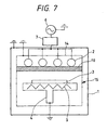
- Fig. 7 is a view showing a longitudinal cross-section of a plasma processing apparatus according to a modification of the apparatus of Fig. 4.
- a parallel-plate-type plasma processing apparatus as shown in Fig. 7 comprises a reaction vessel 15 whose upper portion is constituted by a dielectric member 10 and which can be reduced in pressure.
- the reaction vessel 15 is surrounded by an earth shield 1.
- a plurality of cathode electrodes 2 are arranged on the outside surface (surface on the atmospheric-air side) of the dielectric member 10. More specifically, the cathode electrodes 2 are arranged outside the reaction vessel 15.
- a plate-like substrate 3 serving as a counter electrode of the cathode electrodes 2 is arranged.
- the substrate 3 is heated from its inside to a predetermined temperature by a heater 5 arranged in the reaction vessel 15, and is held by a substrate holder 4 having a rotating mechanism driven by a motor 12.
- the substrate 3 and the substrate holder 4 for holding the substrate 3 is earthed and the substrate 3 is used as the counter electrode of the cathode electrodes 2.
- An evacuation means (not shown) for evacuating the reaction vessel 15 which is partially constituted by the dielectric member 10 and a gas supply means (not shown) for supplying a gas into the reaction vessel 15 are attached to the plasma processing apparatus.
- a matching circuit 7 arranged outside the first earth shield 1 is connected to the cathode electrodes 2, and a high-frequency wave power source 6 is connected to the matching circuit 7.
- a second earth shield 14 is arranged covering the reaction vessel 15 having the plurality of cathode electrodes 2 arranged outside except for high-frequency wave transmission paths extending from the matching circuit 7 to the cathode electrodes 2.
- a plurality of openings (not shown) for connecting the high-frequency wave transmission paths from the outside of the second earth shield 14 to the cathode electrodes 2 are formed in the second earth shield 14.
- Fig. 8 is a view showing the arrangement of a side cross-section of another plasma processing apparatus
- Fig. 9 is another view showing the longitudinal cross-section of this apparatus.
- the same reference numerals as used in Figs. 1 to 7 denote the same parts in Figs. 8 and 9.
- This plasma processing apparatus comprises, as shown in Figs. 8 and 9, a cylindrical dielectric member 10 constituting the side portion of a reaction vessel 15 which can be reduced in pressure, and a first earth shield 1, for preventing high-frequency wave leakage, which forms the upper and bottom portions of the reaction vessel 15 and surrounds the side portion of the reaction vessel 15.
- a cylindrical dielectric member 10 constituting the side portion of a reaction vessel 15 which can be reduced in pressure
- a first earth shield 1 for preventing high-frequency wave leakage, which forms the upper and bottom portions of the reaction vessel 15 and surrounds the side portion of the reaction vessel 15.
- cathode electrodes 2 are arranged to be electrically insulated from the first earth shield 1 by an insulating material 13. More specifically, the cathode electrodes 2 are arranged outside the reaction vessel 15.
- a cylindrical substrate 3 serving as a counter electrode of the cathode electrodes 2 is arranged.
- the substrate 3 is heated from its inside to a predetermined temperature by a heater 5 arranged in the reaction vessel 15, and is held by a substrate holder 4 having a rotating mechanism driven by a motor (not shown).
- the substrate holder 4 for holding the substrate 3 is earthed, and the substrate 3 is used as the counter electrode of the cathode electrodes 2.
- a matching circuit 7 arranged outside the first earth shield 1 is connected to the cathode electrodes 2 through capacitors 11, and a high-frequency wave power source 6 is connected to the matching circuit 7.
- An evacuation means 8 for evacuating the reaction vessel 15 which is partially constituted by the dielectric member 10 and a gas supply means 9 for supplying a gas into the reaction vessel 15 are attached to the plasma processing apparatus.
- a second earth shield 14 is arranged covering the reaction vessel 15 having the plurality of cathode electrodes 2 arranged outside except for high-frequency wave transmission paths extending from the matching circuit 7 to the cathode electrodes 2.
- a plurality of openings (not shown) for connecting the high-frequency wave transmission paths from the outside of the second earth shield 14 to the cathode electrodes 2 are formed in the second earth shield 14.
- the reaction vessel having a plurality of cathode electrodes arranged outside is covered with the earth shields outside the high-frequency wave transmission paths extending from the matching circuit to the cathode electrodes, so that the high-frequency wave power can be prevented from being transmitted to the interior of the reaction vessel through the atmospheric air.
- the substrates to be processed are each cylindrical, and the substrates to be processed and the reaction vessel are arranged on a concentric circle, very uniform deposition films can be formed on the plurality of substrates to be processed at a high speed.
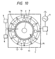
- the number of cathode electrodes need not be limited to two, and, as shown in Fig. 10, a greater plurality of cathode electrodes are preferably arranged to prevent a high-frequency stationary wave from easily occurring and to make the plasma distribution more uniform.
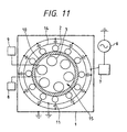
- the apparatus shown in Fig. 10 is modified so that a plurality of substrates 3 are arranged on a concentric circle as shown in Fig. 11. A nonuniform film is rarely formed.
- Fig. 12 is a . view showing a longitudinal cross-section of yet another plasma processing apparatus.
- a parallel-plate-type plasma processing apparatus as shown in Fig. 12 comprises a reaction vessel 15 whose upper portion is constituted by a dielectric member 10 and which can be reduced in pressure.
- the reaction vessel 15 is surrounded by an earth shield 1.
- a plurality of cathode electrodes 2 are arranged on the outside surface (surface on the atmospheric-air side) of the dielectric member 10. More specifically, the cathode electrodes 2 are arranged outside the reaction vessel 15.
- a plate-like film-formed substrate 3 serving as a counter electrode of the cathode electrodes 2 is arranged inside the reaction vessel 15 whose upper portion is constituted by the dielectric member 10.
- the substrate 3 is heated from its inside to a predetermined temperature by a heater 5 arranged in the reaction vessel 15, and is held by a substrate holder 4 having a rotating mechanism driven by a motor (not shown).
- the substrate holder 4 for holding the film-formed substrate 3 is earthed and the film-formed substrate 3 is used as the counter electrode of the cathode electrodes 2.
- An evacuation means (not shown) for evacuating the reaction vessel 15 which is partially constituted by the dielectric member 10 and a gas supply means (not shown) for supplying a gas into the reaction vessel 15 are attached to the plasma processing apparatus.
- a matching circuit 7 arranged outside the first earth shield 1 is connected to the cathode electrodes 2 through capacitors 11, and a high-frequency wave power source 6 is connected to the matching circuit 7.
- the capacitances of the capacitors 11 connected between the matching circuit 7 and the cathode electrodes 2 are changed to values which cancel L components of the transmission paths extending from the matching circuit 7 to the cathode electrodes 2.
- a second earth shield 14 is arranged covering the reaction vessel 15 having the plurality of cathode electrodes 2 arranged thereoutside except for high-frequency wave transmission paths extending from the matching circuit 7 to the cathode electrodes 2.
- a plurality of openings (not shown) for connecting the high-frequency wave transmission paths from the outside of the second earth shield 14 to the cathode electrodes 2 are formed in the second earth shield 14.
- a cathode electrode As a cathode electrode, a right cylindrical Al cathode electrode having an inner diameter of 250 mm and a length of 300 mm was used. The cathode electrode was arranged outside an alumina-ceramic dielectric tube which partially constituted a reaction vessel and had a thickness of 10 mm.
- Film thickness nonuniformity was obtained when film formation was performed by using the externally arranged cathode electrodes.
- a comparison experiment for a film thickness nonuniformity obtained in a case wherein simply cylindrical Al cathode electrodes having an inner diameter of 250 mm and a length of 300 mm was arranged in a reaction vessel was performed.
- the film thickness nonuniformities were about ⁇ 15% in use of the externally arranged cathode electrodes and about ⁇ 30% in use of the cylindrical cathode.
- An effect of improving a film thickness distribution obtained by using the externally arranged cathode electrodes could be confirmed.
- the respective films were considerably influenced by plasma distribution.
- the a-Si film could be sufficient in practical use, e.g., in an electrophotographic photosensitive device, an image input line sensor, or the like.
- the high-frequency wave power source 6 having a frequency of 105 MHz was used, and a discharge experiment was performed under the conditions shown in Table 1 of Example 1.
- the reactance L between the matching circuit and the load was set to 404.5 nH, and a high-power capacitor was arranged as shown in Fig. 1.
- the obtained results are shown in Table 2.
- a rectangular substrate was used. Capacitors were interposed between the matching circuit and cathode electrodes, and the cathode electrodes were arranged outside an alumina-ceramic dielectric rectangular member which partially constituted a reaction vessel and had a thickness of 20 mm. For comparison, the film thickness nonuniformity obtained when the cathode electrodes were arranged inside the reaction vessel to perform film formation under the conditions shown in Table 3 was measured. When the cathode electrodes were arranged outside the reaction vessel, and the capacitors were interposed, the film thickness nonuniformity was about ⁇ 18%; when the cathode electrodes were arranged inside the reaction vessel, the film thickness nonuniformity was about ⁇ 35%.
- the respective films were considerably influenced by plasma distribution.
- the a-Si film could be sufficient in practical use, e.g., in an electrophotographic photosensitive device, an image input line sensor, or the like.
- the film thickness nonuniformity obtained when a film forming apparatus having the second earth shield was measured. As a result, the film thickness nonuniformity was about ⁇ 11%. When the second earth shield was not used, the film thickness nonuniformity was about ⁇ 15%. It was confirmed that an effect of improving the film thickness distribution was obtained by using the second earth shield.
- the respective films were considerably influenced by plasma distribution.
- the a-Si film could be sufficient in practical use, e.g., in an electrophotographic photosensitive device, an image input line sensor, or the like.
- the second earth shield covering a reaction vessel having the plurality of cathode electrodes arranged outside except for high-frequency wave transmission paths extending from the matching circuit to the cathode electrodes, a complex impedance at a high frequency can be increased.
- the arrangement is designed such that only a portion of the high-frequency path free from the earth shield can be controlled, a problem of film thickness nonuniformity caused by a high discharge frequency can be solved.
- the film thickness nonuniformity was measured by using an apparatus in which the second earth shield was arranged. As a result, the film thickness nonuniformity was about ⁇ 13% in comparison with about ⁇ 18% obtained by using a simple plate, and preferable film thickness uniformity was exhibited.
- the respective films were considerably influenced by plasma distribution.
- the a-Si film could be sufficient in practical use, e.g., in an electrophotographic photosensitive device, an image input line sensor, or the like.
- cathode electrodes right cylindrical Al cathode electrodes each having an inner diameter of 250 mm and a length of 300 mm were used.
- the cathode electrodes were arranged outside an alumina-ceramic dielectric tube which partially constituted a reaction vessel and had a thickness of 10 mm.
- a second earth shield was arranged covering the reaction vessel having the plurality of cathode electrodes arranged outside except for high-frequency wave transmission paths extending from the matching circuit to the cathode electrodes.
- the cathode length was not limited to the value in this example.
- the film thickness nonuniformity was obtained when film formation was performed by using the externally arranged cathode electrode.
- comparison experiments were performed to measure film thickness nonuniformities: in a case wherein right cylindrical Al cathode electrodes each having a length of 300 mm were arranged in a reaction vessel a case wherein externally arranged cathodes shown in Fig. 1 were used, and capacitors were interposed between the matching circuit and the cathodes; and a case wherein a second earth shield covering the reaction vessel having the plurality of cathode electrodes arranged outside except for high-frequency wave transmission paths extending from the matching circuit to the cathode electrodes.
- the film thickness nonuniformity was about ⁇ 15% when cylindrical cathode electrodes were arranged in the reaction vessel; ⁇ 13% when the capacitors were interposed; ⁇ 11% when the second earth shield was interposed; and ⁇ 9% when the apparatus using the capacitors and the second earth shield was used. The effect of improving the film thickness distribution was confirmed.
- the respective films were considerably influenced by plasma distribution.
- the a-Si film could be sufficient in practical use, e.g., in an electrophotographic photosensitive device, an image input line sensor, or the like.
- the capacitors are arranged between the cathode electrodes and the matching circuit
- the second earth shield is arranged covering the reaction vessel having the plurality of cathode electrodes arranged outside except for high-frequency wave transmission paths extending from the matching circuit to the cathode electrodes, and a high-frequency wave is supplied to the plasma through the dielectric member partially constituting the reaction chamber which can be reduced in pressure.
- matching can be established, and loss caused by transmission of the high-frequency wave power through the atmospheric air before the high-frequency wave power reaches the cathode electrodes is maximally prevented, so that the plasma is stable.
- the problem of film thickness nonuniformity can be solved.
- the entire film nonuniformity was about 12%, and the film quality could be sufficient in practical use, e.g., in an electrophotographic photosensitive device, an image input line sensor, or the like. Therefore, an apparatus having high productivity can be provided.
- a parallel-plate-type plasma CVD apparatus having a second earth shield covering a reaction vessel having a plurality of cathode electrodes arranged outside except for high-frequency wave transmission paths extending from a matching circuit to the cathode electrodes and capacitors interposed between a matching circuit and the cathode electrodes, an a-Si film was formed on the film-formed substrate at a discharge frequency of 100 MHz under the film-formation conditions shown in Table 3, and the film thickness nonuniformity was measured.
- the film thickness nonuniformity was about ⁇ 10%, in comparison with about ⁇ 18% obtained by using a simple plate, and better film thickness uniformity was exhibited.
- the respective films were considerably influenced by plasma distribution.
- the a-Si film could be sufficient in practical use, e.g., in an electrophotographic photosensitive device, an image input line sensor, or the like.
- An a-Si film formed in this example had film quality higher than that of an a-Si film formed by a conventional apparatus and nonuniformity less than that of the a-Si film formed by the conventional apparatus.
- the a-Si film formed in this example could be sufficient in practical use, e.g., in an electrophotographic photosensitive device, an image input line sensor, or the like.
- a high-frequency wave power having 30 MHz or higher and 600 MHz or lower is supplied to the cathode electrodes through a matching circuit to generate a plasma between the cathode electrodes and the counter electrode, and a plasma process is performed to a substrate to be processed arranged on the counter electrode, the plurality of cathode electrodes are arranged outside the reaction vessel, and the reaction vessel between the cathode electrodes and the counter electrode is partially constituted by a dielectric member, so that homogeneous high-frequency wave discharge having a large area can be easily achieved, and a plasma process for a large substrate can be uniformly performed at a high speed.
- the dielectric material buffers the non-uniformity of the high-frequency wave voltage on the cathode electrodes to make the plasma distribution uniform. For this reason, a uniform plasma can be supplied to a substrate to be processed.
- the cathode electrodes are arranged outside the reaction vessel, the degree of freedom of the design of the cathode electrodes increases, and the optimum shape and optimum constituent material of the cathode electrode can be easily determined.
- high-frequency wave power is separately supplied to a plurality of cathode electrodes, a high-frequency stationary wave can be prevented from easily occurring by decreasing the surface area per cathode, and the arrangement is optimum to form a large-area plasma.
- the transmission paths between the matching circuit and the cathode electrodes are different from each other in length, and inductances L of the transmission paths are different from each other. For this reason, matching may not be established at a high frequency.
- capacitors are arranged in the high-frequency wave transmission paths between the matching circuit and the cathode electrodes, the L components can be cancelled and the matching can be reliably established.
- the apparatus has an earth shield covering a reaction vessel having the cathode electrodes arranged outside except for high-frequency wave transmission paths extending from the matching circuit to the cathode electrodes, the high-frequency wave power is prevented from being transmitted to the interior of the reaction vessel through the matching circuit and the atmospheric air in the middle of the high-frequency wave transmission paths. For this reason, the plasma distribution can be prevented from being nonuniform.
Landscapes
- Chemical & Material Sciences (AREA)
- Engineering & Computer Science (AREA)
- Physics & Mathematics (AREA)
- Plasma & Fusion (AREA)
- Analytical Chemistry (AREA)
- Mechanical Engineering (AREA)
- Organic Chemistry (AREA)
- Metallurgy (AREA)
- Materials Engineering (AREA)
- Chemical Kinetics & Catalysis (AREA)
- General Chemical & Material Sciences (AREA)
- Power Engineering (AREA)
- Plasma Technology (AREA)
- Drying Of Semiconductors (AREA)
- Chemical Vapour Deposition (AREA)
- ing And Chemical Polishing (AREA)
- Physical Deposition Of Substances That Are Components Of Semiconductor Devices (AREA)
Claims (14)
- Appareil de traitement par plasma comportant:caractérisé en ce que ledit support (4) de substrat est l'un d'une pluralité et la pluralité de supports (4) de substrat sont espacés sur la circonférence d'un cercle ayant un premier diamètre, et en ce que ladite pluralité d'électrodes de cathode (2) sont espacées sur la circonférence d'un cercle concentrique ayant un second diamètre supérieur au premier diamètre.une enceinte de réaction (15) dont la pression interne peut être abaissée, au moins une partie (10) de ladite enceinte de réaction étant formée d'une matière diélectrique;un support (4) de substrat sur lequel un substrat (3) devant être traité est destiné à être agencé, ledit support de substrat étant agencé dans ladite enceinte de réaction;un moyen (9) pour alimenter ladite enceinte de réaction en un gaz de traitement; etune pluralité d'électrodes (2) de cathode, connectées à un circuit d'adaptation (7), pour l'introduction d'une énergie ondulatoire à haute fréquence à l'intérieur de ladite enceinte de réaction en passant par ledit circuit d'adaptation depuis une source d'énergie ondulatoire à haute fréquence (6), ladite pluralité d'électrodes de cathode étant agencée sur l'extérieur de ladite enceinte de réaction;
- Appareil de traitement par plasma selon la revendication 1, dans lequel chacune de ladite pluralité d'électrodes de cathode (2) est connectée audit circuit d'adaptation (7) par l'intermédiaire d'un condensateur respectif (11).
- Appareil de traitement par plasma selon l'une des revendications 1 ou 2, dans lequel ladite matière diélectrique (10) est choisie parmi l'un quelconque d'une céramique d'alumine, du verre ou de polytétrafluoréthylène.
- Appareil de traitement par plasma selon l'une quelconque des revendications précédentes, comprenant une source (6) d'énergie ondulatoire à haute fréquence, dans laquelle ladite énergie ondulatoire à haute fréquence a une fréquence de 30 MHz à 600 MHz.
- Appareil de traitement par plasma selon l'une quelconque des revendications précédentes, comportant un premier blindage (4) de terre renfermant ladite enceinte de réaction et ladite pluralité d'électrodes de cathode.
- Appareil de traitement par plasma selon la revendication 5, comportant un second blindage (1) de terre recouvrant un trajet pour connecter ladite pluralité d'électrodes de cathode (2) et ledit circuit d'adaptation (7) entre eux et recouvrant ledit premier blindage de terre (14).
- Procédé de traitement par plasma, caractérisé en ce qu'il comprend les étapes dans lesquelles:on dispose des substrats (3) devant être traités sur une pluralité de supports (4) de substrats espacés le long de la circonférence d'un cercle concentrique ayant un premier diamètre dans une enceinte (15) de réaction dont la pression interne peut être abaissée, au moins une partie (10) de ladite enceinte de réaction étant formée d'une matière diélectrique;on alimente ladite enceinte de réaction en un gaz de traitement;on introduit une onde à haute fréquence à l'intérieur de ladite enceinte de réaction en passant par un circuit d'adaptation (7) connecté à une pluralité d'électrodes de cathode (2) qui sont disposées sur l'extérieur de ladite enceinte de réaction et espacées sur la circonférence d'un cercle ayant un second diamètre supérieur au premier diamètre pour générer ainsi un plasma dans ladite enceinte de réaction; eton soumet ladite pluralité de substrats à un traitement par plasma.
- Procédé de traitement par plasma selon la revendication 7, dans lequel chacune de ladite pluralité d'électrodes de cathode (2) est connectée audit circuit d'adaptation (7) par l'intermédiaire d'un condensateur respectif (11).
- Procédé de traitement par plasma selon l'une des revendications 7 ou 8, dans lequel ladite matière diélectrique (10) est choisie parmi l'un quelconque d'une céramique d'alumine, du verre ou du polytétrafluoréthylène.
- Procédé de traitement par plasma selon l'une quelconque des revendications 7 à 9, dans lequel ladite énergie ondulatoire à haute fréquence a une fréquence de 30 MHz à 600 MHz.
- Procédé de traitement par plasma selon l'une quelconque des revendications 7 à 10, exécuté avec un premier blindage (14) de terre renfermant ladite enceinte de réaction et ladite pluralité d'électrodes de cathode.
- Procédé de traitement par plasma selon la revendication 11, exécuté avec un second blindage (1) de terre recouvrant un trajet destiné à connecter ladite pluralité d'électrodes de cathode (2) et ledit circuit d'adaptation (7) entre eux et recouvrant ledit premier blindage (14) de terre.
- Procédé de traitement par plasma selon l'une quelconque des revendications 7 à 12, dans lequel ledit traitement par plasma est l'un quelconque de: un dépôt chimique en phase vapeur; une pulvérisation; une attaque chimique; ou une calcination.
- Procédé de production de dispositifs photosensibles électrophotographiques ou de production de capteurs de ligne d'entrée d'image, qui comprend la production d'un film de α-Si sur une pluralité de substrats par le procédé selon l'une quelconque des revendications 7 à 13 puis l'utilisation du film de α-Si déposé dans la production des dispositifs ou des capteurs.
Applications Claiming Priority (3)
| Application Number | Priority Date | Filing Date | Title |
|---|---|---|---|
| JP12577096 | 1996-05-21 | ||
| JP125770/96 | 1996-05-21 | ||
| JP12577096A JP3437376B2 (ja) | 1996-05-21 | 1996-05-21 | プラズマ処理装置及び処理方法 |
Publications (3)
| Publication Number | Publication Date |
|---|---|
| EP0808918A2 EP0808918A2 (fr) | 1997-11-26 |
| EP0808918A3 EP0808918A3 (fr) | 1998-10-28 |
| EP0808918B1 true EP0808918B1 (fr) | 2002-10-02 |
Family
ID=14918408
Family Applications (1)
| Application Number | Title | Priority Date | Filing Date |
|---|---|---|---|
| EP97303434A Expired - Lifetime EP0808918B1 (fr) | 1996-05-21 | 1997-05-20 | Appareillage de traitement par plasma et méthode de traitement |
Country Status (5)
| Country | Link |
|---|---|
| US (2) | US6145469A (fr) |
| EP (1) | EP0808918B1 (fr) |
| JP (1) | JP3437376B2 (fr) |
| KR (1) | KR100276599B1 (fr) |
| DE (1) | DE69715962T2 (fr) |
Families Citing this family (19)
| Publication number | Priority date | Publication date | Assignee | Title |
|---|---|---|---|---|
| JP3437376B2 (ja) * | 1996-05-21 | 2003-08-18 | キヤノン株式会社 | プラズマ処理装置及び処理方法 |
| JP2921499B2 (ja) * | 1996-07-30 | 1999-07-19 | 日本電気株式会社 | プラズマ処理装置 |
| AU2001224729A1 (en) * | 2000-01-10 | 2001-07-24 | Tokyo Electron Limited | Segmented electrode assembly and method for plasma processing |
| JP2001323379A (ja) | 2000-05-15 | 2001-11-22 | Canon Inc | 堆積膜形成装置および堆積膜形成方法 |
| JP2002030447A (ja) * | 2000-07-11 | 2002-01-31 | Canon Inc | プラズマ処理方法及びプラズマ処理装置 |
| KR100829327B1 (ko) * | 2002-04-05 | 2008-05-13 | 가부시키가이샤 히다치 고쿠사이 덴키 | 기판 처리 장치 및 반응 용기 |
| JP4226597B2 (ja) * | 2003-03-04 | 2009-02-18 | 株式会社日立国際電気 | 基板処理装置およびデバイスの製造方法 |
| JP4298401B2 (ja) * | 2003-06-27 | 2009-07-22 | キヤノン株式会社 | 堆積膜形成装置、及び堆積膜形成方法 |
| DE102004009735A1 (de) * | 2004-02-25 | 2005-09-15 | Endress + Hauser Gmbh + Co. Kg | Meßgerät mit Anzeigevorrichtung |
| US20070048456A1 (en) * | 2004-09-14 | 2007-03-01 | Keshner Marvin S | Plasma enhanced chemical vapor deposition apparatus and method |
| KR100909750B1 (ko) * | 2005-03-01 | 2009-07-29 | 가부시키가이샤 히다치 고쿠사이 덴키 | 기판 처리 장치 및 반도체 디바이스의 제조 방법 |
| US8176871B2 (en) * | 2006-03-28 | 2012-05-15 | Hitachi Kokusai Electric Inc. | Substrate processing apparatus |
| US20080139003A1 (en) * | 2006-10-26 | 2008-06-12 | Shahid Pirzada | Barrier coating deposition for thin film devices using plasma enhanced chemical vapor deposition process |
| JP5568212B2 (ja) * | 2007-09-19 | 2014-08-06 | 株式会社日立国際電気 | 基板処理装置、そのコーティング方法、基板処理方法及び半導体デバイスの製造方法 |
| TWI477646B (zh) * | 2010-08-09 | 2015-03-21 | Hon Hai Prec Ind Co Ltd | 化學氣相沉積設備 |
| JP5730521B2 (ja) * | 2010-09-08 | 2015-06-10 | 株式会社日立ハイテクノロジーズ | 熱処理装置 |
| US9868653B2 (en) * | 2013-05-01 | 2018-01-16 | Nch Corporation | System and method for treating water systems with high voltage discharge and ozone |
| US9932252B2 (en) | 2013-05-01 | 2018-04-03 | Nch Corporation | System and method for treating water systems with high voltage discharge and ozone |
| US11390950B2 (en) * | 2017-01-10 | 2022-07-19 | Asm Ip Holding B.V. | Reactor system and method to reduce residue buildup during a film deposition process |
Family Cites Families (14)
| Publication number | Priority date | Publication date | Assignee | Title |
|---|---|---|---|---|
| US4158717A (en) * | 1977-02-14 | 1979-06-19 | Varian Associates, Inc. | Silicon nitride film and method of deposition |
| GB2018446B (en) * | 1978-03-03 | 1983-02-23 | Canon Kk | Image-forming member for electrophotography |
| US4664890A (en) * | 1984-06-22 | 1987-05-12 | Kanegafuchi Kagaku Kogyo Kabushiki Kaisha | Glow-discharge decomposition apparatus |
| JPH04362091A (ja) * | 1991-06-05 | 1992-12-15 | Mitsubishi Heavy Ind Ltd | プラズマ化学気相成長装置 |
| US5383984A (en) * | 1992-06-17 | 1995-01-24 | Tokyo Electron Limited | Plasma processing apparatus etching tunnel-type |
| US5277751A (en) * | 1992-06-18 | 1994-01-11 | Ogle John S | Method and apparatus for producing low pressure planar plasma using a coil with its axis parallel to the surface of a coupling window |
| TW249313B (fr) * | 1993-03-06 | 1995-06-11 | Tokyo Electron Co | |
| WO2004083486A1 (fr) * | 1993-03-23 | 2004-09-30 | Atsushi Yamagami | Procede et appareil pour depot chimique en phase vapeur par plasma au moyen d'onde ultracourte |
| US5531834A (en) * | 1993-07-13 | 1996-07-02 | Tokyo Electron Kabushiki Kaisha | Plasma film forming method and apparatus and plasma processing apparatus |
| KR100276736B1 (ko) * | 1993-10-20 | 2001-03-02 | 히가시 데쓰로 | 플라즈마 처리장치 |
| US5653811A (en) * | 1995-07-19 | 1997-08-05 | Chan; Chung | System for the plasma treatment of large area substrates |
| US6065425A (en) | 1996-03-25 | 2000-05-23 | Canon Kabushiki Kaisha | Plasma process apparatus and plasma process method |
| JP3437376B2 (ja) * | 1996-05-21 | 2003-08-18 | キヤノン株式会社 | プラズマ処理装置及び処理方法 |
| US5970907A (en) | 1997-01-27 | 1999-10-26 | Canon Kabushiki Kaisha | Plasma processing apparatus |
-
1996
- 1996-05-21 JP JP12577096A patent/JP3437376B2/ja not_active Expired - Fee Related
-
1997
- 1997-05-09 US US08/853,449 patent/US6145469A/en not_active Expired - Lifetime
- 1997-05-20 DE DE69715962T patent/DE69715962T2/de not_active Expired - Lifetime
- 1997-05-20 EP EP97303434A patent/EP0808918B1/fr not_active Expired - Lifetime
- 1997-05-21 KR KR1019970019765A patent/KR100276599B1/ko not_active Expired - Fee Related
-
2000
- 2000-09-18 US US09/664,339 patent/US6558507B1/en not_active Expired - Fee Related
Also Published As
| Publication number | Publication date |
|---|---|
| EP0808918A3 (fr) | 1998-10-28 |
| KR100276599B1 (ko) | 2000-12-15 |
| DE69715962D1 (de) | 2002-11-07 |
| US6558507B1 (en) | 2003-05-06 |
| EP0808918A2 (fr) | 1997-11-26 |
| US6145469A (en) | 2000-11-14 |
| JP3437376B2 (ja) | 2003-08-18 |
| DE69715962T2 (de) | 2003-06-18 |
| JPH09310181A (ja) | 1997-12-02 |
| KR970077336A (ko) | 1997-12-12 |
Similar Documents
| Publication | Publication Date | Title |
|---|---|---|
| EP0808918B1 (fr) | Appareillage de traitement par plasma et méthode de traitement | |
| US6065425A (en) | Plasma process apparatus and plasma process method | |
| JP3236111B2 (ja) | プラズマ処理装置及び処理方法 | |
| HK1046774B (zh) | 用於处理具有大表面的衬底的等离子反应器 | |
| JP3501668B2 (ja) | プラズマcvd方法及びプラズマcvd装置 | |
| EP2113937A1 (fr) | Appareil de traitement sous vide et procédé de fabrication de film utilisant l'appareil de traitement sous vide | |
| US5970907A (en) | Plasma processing apparatus | |
| US5846612A (en) | Process for forming high-quality deposited film utilizing plasma CVD | |
| US5558719A (en) | Plasma processing apparatus | |
| JPH0776781A (ja) | プラズマ気相成長装置 | |
| US5718769A (en) | Plasma processing apparatus | |
| EP0678895B1 (fr) | Appareil de traitement par plasma | |
| JPH06295866A (ja) | プラズマ反応装置 | |
| GB2286200A (en) | Plasma treatment of substrates having non planar surfaces; contoured electrodes | |
| JP3793034B2 (ja) | プラズマcvd装置 | |
| KR100269930B1 (ko) | 플라즈마 처리장치 및 플라즈마 처리방법 | |
| JPH05343338A (ja) | プラズマcvd装置 | |
| JP4355490B2 (ja) | 堆積膜形成装置 | |
| JP2001335944A (ja) | プラズマ処理装置およびプラズマ処理方法 | |
| JP2002030449A (ja) | 結晶性シリコン膜、結晶性シリコン膜の形成方法及び結晶性シリコン膜の形成装置 | |
| JPH08339963A (ja) | プラズマ処理装置および処理方法 | |
| JP2626203B2 (ja) | 電子写真感光体の製造方法 | |
| US6486045B2 (en) | Apparatus and method for forming deposited film | |
| JPH01279757A (ja) | プラズマ処理装置 | |
| JPH05291149A (ja) | プラズマcvd装置 |
Legal Events
| Date | Code | Title | Description |
|---|---|---|---|
| PUAI | Public reference made under article 153(3) epc to a published international application that has entered the european phase |
Free format text: ORIGINAL CODE: 0009012 |
|
| AK | Designated contracting states |
Kind code of ref document: A2 Designated state(s): DE FR GB IT NL |
|
| PUAL | Search report despatched |
Free format text: ORIGINAL CODE: 0009013 |
|
| AK | Designated contracting states |
Kind code of ref document: A3 Designated state(s): DE FR GB IT NL |
|
| 17P | Request for examination filed |
Effective date: 19990310 |
|
| 17Q | First examination report despatched |
Effective date: 20000426 |
|
| GRAG | Despatch of communication of intention to grant |
Free format text: ORIGINAL CODE: EPIDOS AGRA |
|
| GRAG | Despatch of communication of intention to grant |
Free format text: ORIGINAL CODE: EPIDOS AGRA |
|
| GRAH | Despatch of communication of intention to grant a patent |
Free format text: ORIGINAL CODE: EPIDOS IGRA |
|
| GRAH | Despatch of communication of intention to grant a patent |
Free format text: ORIGINAL CODE: EPIDOS IGRA |
|
| GRAA | (expected) grant |
Free format text: ORIGINAL CODE: 0009210 |
|
| AK | Designated contracting states |
Kind code of ref document: B1 Designated state(s): DE FR GB IT NL |
|
| PG25 | Lapsed in a contracting state [announced via postgrant information from national office to epo] |
Ref country code: NL Free format text: LAPSE BECAUSE OF FAILURE TO SUBMIT A TRANSLATION OF THE DESCRIPTION OR TO PAY THE FEE WITHIN THE PRESCRIBED TIME-LIMIT Effective date: 20021002 Ref country code: IT Free format text: LAPSE BECAUSE OF FAILURE TO SUBMIT A TRANSLATION OF THE DESCRIPTION OR TO PAY THE FEE WITHIN THE PRE;WARNING: LAPSES OF ITALIAN PATENTS WITH EFFECTIVE DATE BEFORE 2007 MAY HAVE OCCURRED AT ANY TIME BEFORE 2007. THE CORRECT EFFECTIVE DATE MAY BE DIFFERENT FROM THE ONE RECORDED.SCRIBED TIME-LIMIT Effective date: 20021002 Ref country code: FR Free format text: LAPSE BECAUSE OF FAILURE TO SUBMIT A TRANSLATION OF THE DESCRIPTION OR TO PAY THE FEE WITHIN THE PRESCRIBED TIME-LIMIT Effective date: 20021002 |
|
| REG | Reference to a national code |
Ref country code: GB Ref legal event code: FG4D |
|
| REF | Corresponds to: |
Ref document number: 69715962 Country of ref document: DE Date of ref document: 20021107 |
|
| NLV1 | Nl: lapsed or annulled due to failure to fulfill the requirements of art. 29p and 29m of the patents act | ||
| PG25 | Lapsed in a contracting state [announced via postgrant information from national office to epo] |
Ref country code: GB Free format text: LAPSE BECAUSE OF NON-PAYMENT OF DUE FEES Effective date: 20030520 |
|
| EN | Fr: translation not filed | ||
| PLBE | No opposition filed within time limit |
Free format text: ORIGINAL CODE: 0009261 |
|
| STAA | Information on the status of an ep patent application or granted ep patent |
Free format text: STATUS: NO OPPOSITION FILED WITHIN TIME LIMIT |
|
| 26N | No opposition filed |
Effective date: 20030703 |
|
| GBPC | Gb: european patent ceased through non-payment of renewal fee |
Effective date: 20030520 |
|
| PGFP | Annual fee paid to national office [announced via postgrant information from national office to epo] |
Ref country code: DE Payment date: 20140531 Year of fee payment: 18 |
|
| REG | Reference to a national code |
Ref country code: DE Ref legal event code: R119 Ref document number: 69715962 Country of ref document: DE |
|
| PG25 | Lapsed in a contracting state [announced via postgrant information from national office to epo] |
Ref country code: DE Free format text: LAPSE BECAUSE OF NON-PAYMENT OF DUE FEES Effective date: 20151201 |