EP0804000B1 - Dispositif de détection de signaux RDS - Google Patents
Dispositif de détection de signaux RDS Download PDFInfo
- Publication number
- EP0804000B1 EP0804000B1 EP97302747A EP97302747A EP0804000B1 EP 0804000 B1 EP0804000 B1 EP 0804000B1 EP 97302747 A EP97302747 A EP 97302747A EP 97302747 A EP97302747 A EP 97302747A EP 0804000 B1 EP0804000 B1 EP 0804000B1
- Authority
- EP
- European Patent Office
- Prior art keywords
- signals
- biphase
- circuit
- rds
- signal
- Prior art date
- Legal status (The legal status is an assumption and is not a legal conclusion. Google has not performed a legal analysis and makes no representation as to the accuracy of the status listed.)
- Expired - Lifetime
Links
Images


Classifications
-
- H—ELECTRICITY
- H04—ELECTRIC COMMUNICATION TECHNIQUE
- H04L—TRANSMISSION OF DIGITAL INFORMATION, e.g. TELEGRAPHIC COMMUNICATION
- H04L27/00—Modulated-carrier systems
- H04L27/18—Phase-modulated carrier systems, i.e. using phase-shift keying
- H04L27/22—Demodulator circuits; Receiver circuits
- H04L27/233—Demodulator circuits; Receiver circuits using non-coherent demodulation
- H04L27/2332—Demodulator circuits; Receiver circuits using non-coherent demodulation using a non-coherent carrier
-
- H—ELECTRICITY
- H04—ELECTRIC COMMUNICATION TECHNIQUE
- H04H—BROADCAST COMMUNICATION
- H04H60/00—Arrangements for broadcast applications with a direct linking to broadcast information or broadcast space-time; Broadcast-related systems
- H04H60/35—Arrangements for identifying or recognising characteristics with a direct linkage to broadcast information or to broadcast space-time, e.g. for identifying broadcast stations or for identifying users
- H04H60/38—Arrangements for identifying or recognising characteristics with a direct linkage to broadcast information or to broadcast space-time, e.g. for identifying broadcast stations or for identifying users for identifying broadcast time or space
- H04H60/41—Arrangements for identifying or recognising characteristics with a direct linkage to broadcast information or to broadcast space-time, e.g. for identifying broadcast stations or for identifying users for identifying broadcast time or space for identifying broadcast space, i.e. broadcast channels, broadcast stations or broadcast areas
- H04H60/44—Arrangements for identifying or recognising characteristics with a direct linkage to broadcast information or to broadcast space-time, e.g. for identifying broadcast stations or for identifying users for identifying broadcast time or space for identifying broadcast space, i.e. broadcast channels, broadcast stations or broadcast areas for identifying broadcast stations
-
- H—ELECTRICITY
- H04—ELECTRIC COMMUNICATION TECHNIQUE
- H04H—BROADCAST COMMUNICATION
- H04H20/00—Arrangements for broadcast or for distribution combined with broadcast
- H04H20/20—Arrangements for broadcast or distribution of identical information via plural systems
- H04H20/22—Arrangements for broadcast of identical information via plural broadcast systems
-
- H—ELECTRICITY
- H04—ELECTRIC COMMUNICATION TECHNIQUE
- H04H—BROADCAST COMMUNICATION
- H04H2201/00—Aspects of broadcast communication
- H04H2201/10—Aspects of broadcast communication characterised by the type of broadcast system
- H04H2201/13—Aspects of broadcast communication characterised by the type of broadcast system radio data system/radio broadcast data system [RDS/RBDS]
-
- H—ELECTRICITY
- H04—ELECTRIC COMMUNICATION TECHNIQUE
- H04L—TRANSMISSION OF DIGITAL INFORMATION, e.g. TELEGRAPHIC COMMUNICATION
- H04L27/00—Modulated-carrier systems
- H04L27/0014—Carrier regulation
- H04L2027/0024—Carrier regulation at the receiver end
- H04L2027/0026—Correction of carrier offset
- H04L2027/0028—Correction of carrier offset at passband only
-
- H—ELECTRICITY
- H04—ELECTRIC COMMUNICATION TECHNIQUE
- H04L—TRANSMISSION OF DIGITAL INFORMATION, e.g. TELEGRAPHIC COMMUNICATION
- H04L27/00—Modulated-carrier systems
- H04L27/0014—Carrier regulation
- H04L2027/0044—Control loops for carrier regulation
- H04L2027/0046—Open loops
- H04L2027/0048—Frequency multiplication
Definitions
- the present invention relates to an Radio Data System (RDS) signal detection device incorporated in a device to receive and demodulate RDS broadcasting signals, which judges whether signals received are RDS signals or not.
- RDS Radio Data System
- the reception station selected according to the AF code can be a non-RDS station, or reception sensitivity of the station is sometimes not good enough to receive RDS data.
- a Program Identification code (PI code) for judging whether the station selected is a station to broadcast the same program is not detected, and as a consequence selection of a proper station is not performed. Therefore, re-selection of a station on the AF list having a second best strength of reception electric field is performed. For a quicker, more accurate selection, it is necessary to judge, as soon as possible, whether a station switched to is an RDS station or not. Likewise, if only RDS stations are sought and selected or memorized, it is necessary to judge, as soon as possible, whether the station selected is an RDS station or not.
- a judging action of an RDS station such as that described above has conventionally been performed by detecting block synchronization or group synchronization of RDS data after broadcasting signal reception has been started by the selected station which was assumed to be an AF station.
- the RDS data is configured in blocks of 26 bits.
- a certain synchronization pattern (offset words) is added to each block.
- Block synchronization is established by detecting the periodicity of the patterns.
- One group is configured in four blocks, and group synchronization is established by judging an order of offset words.
- US 5001728 describes an apparatus for demodulating a biphase signal that is arranged to identify a symbol by detecting the rising edge of a received waveform.
- JP 08084161 describes a reception detection circuit using a biphase code where a biphase code is input to three flip flop circuits to allow a determination to be made as to whether a biphase code is received by examining three halfbits.
- US5200980 describes a digital biphase data recovery system that is arranged to identify a symbol by detecting the falling edge of a received waveform.
- EP0717517 describes an apparatus that determines whether a received signal includes a biphase code when a ratio of positive phase symbols and negative phase symbols is 2:1 or 1:2 among three consecutive halfbits.
- RDS signals are differentially coded and then biphase coded to suppress power of signals with closer carrier frequencies.
- biphase coding for example, a signal of data 1 is expressed by (1,0), and (0,1) is for a signal of 0. Therefore, one symbol is converted and coded into two symbols.
- the amplitudes of the carrier frequency signals are modulated by the biphase coding signals. They are then multiplexed into FM base band signals and become actual broadcasting waves.
- the present invention takes advantage of the RDS signals which are biphased, and judges whether received signals are RDS signals or not by detecting the existence of pairs of coded symbols within the received signals.
- the present invention distinguishes RDS signals by first detecting inversion of signals within a biphase symbol pair and then by detecting continuity or a ratio of inversion for a certain duration.
- Another method of RDS signal judgment is to detect, using the same method as described above, stability of output from a pair judgment circuit which detects a combination of biphase symbols.
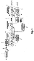
- Fig. 1 is a block diagram of an RDS demodulator related to the present invention.
- FM composite signals in which RDS signals are multiplexed are supplied to a 57KHz-BPF circuit 1.
- RDS signals are then separated by the 57 KHz-BPF circuit 1, and supplied to a comparator 2 where the RDS signals are digitized into 0 or 1.
- Output from the comparator is supplied to both a carrier regenerator circuit 3 and a D flip-flop (hereafter called D-FF) 4 which is a phase detector circuit.
- D-FF D flip-flop
- clock signals synchronizing a carrier of 57 KHz are regenerated at the carrier regenerator circuit 3. Based on the regenerated clock signals, D-FF 4 samples the output from the comparator 2.
- Fig. 6 shows waveforms of signals.
- RDS signals of Fig. 6(a) are output.
- Digital signals (b) are output from the comparator 2.
- Clock signals of 57 KHz regenerated by the carrier regenerator circuit 3 are supplied to the D-FF4 on timings shown in (c) (with 90 ° of phase shift from carrier signals) .
- signals shown in (d) are obtained as the sampling output from the D-FF 4.
- These signals (d) are supplied to both a biphase clock regenerator circuit 5 and a data decision circuit 13. In the biphase clock regenerator circuit 5, clock pulses at a biphase symbol rate shown in (e) are regenerated.
- an adder 6 adds output from a D-FF 7 which the output of the adder 6 is supplied with, and output from the D-FF 4 shown in (d).
- the D-FF 7 is reset by the clock pulses at the biphase symbol rate shown in (e).
- the D-FF 7 and the adder 6 form an accumulator.
- the sampling output data from the D-FF 4 are accumulated by the accumulator for one symbol period. More specifically, the number of "1"s in the sampling output data is accumulated.
- a D-FF 8 latches the accumulation result using the clock pulses shown in (e) at the biphase symbol rate.
- the latched result is input into both a biphase decoder circuit 9 and a data clock regenerator circuit 10.
- the biphase decoder circuit 9 includes both a D-FF 90 which delays the output from the D-FF8 by one biphase period using the clock pulses (e) at the biphase symbol rate, and a subtraction circuit 91 which subtracts the output of the D-FF8 from the output of the D-FF 90.
- a differential process is performed between neighboring biphase symbol data by both the D-FF 90 and the subtraction circuit 91.
- the differentially coded bit is supplied to a D-FF 94 as differentially coded RDS data.
- the biphase symbol data are expressed as (1,0) for source data of 1, and as (0,1) for source data of 0. Therefore, if the differential result is positive, then the differentially coded RDS data is 1. If the differential result is negative, then the differentially coded RDS data is 0.
- the data judgment circuitry 15 if the differential result falls within a range from -5 to +5, assuming that the control data P is ⁇ 5 for example, the input signals are judged not to be biphase coded signals, in other words, not to be RDS signals. The data judgment circuitry 15 then outputs 0 as judgment data. If the differential result does not fall within the previous range, then the data judgment circuitry 15 judges the input signals to be biphase coded RDS signals, and outputs 1 as the judgment data.
- the data clock regenerator circuit 10 judges pairs of biphase symbol data based on the output from the D-FF8. At timings of every other symbol to be paired, the data clock regenerator circuit 10 then separates clock signals from biphase clock signals which were regenerated at each symbol. The data clock regenerator circuit 10 then supplies these clock signals to both D-FFs 94, 16 and also to a differential decoder circuit 11 as data clock signals shown in (g). Therefore, differentially coded RDS data outputted from the subtraction circuit 91 and the judgment data from the data judgment circuitry 15 are latched into D-FFs 94 and 16 at every two biphase symbols constituting a pair.
- the differentially coded RDS data latched into the D-FF 94 are supplied to a differential decoder circuit 11. Consecutive differentially coded RDS data are decoded into RDS source data by a D-FF 110 and an EXOR circuit 112, and then supplied to a later-described synchronization regenerator circuit where synchronization is established based on the RDS source data.
- the judgment data latched into the D-FF 16 are supplied to an RDS-ID detector circuit 14 where the signals input are examined to see whether they are RDS signals or not using the judgment data.
- the accumulator (the adder 6 and the D-FF 7) which simply accumulates sampling data for one symbol period is used in the data decision circuit 13 to obtain an accumulation result of the sampling output.
- a low-pass filter can be substituted for the accumulator, however.
- a digital low-pass filter 12 of 2375 KHz pass band which is the RDS biphase symbol rate is provided instead of the adder 6 and the D-FF 7.
- Sampling output from the D-FF 4 is supplied to the low-pass filter 12.
- the biphase clock regenerator circuit 5 is constructed so that clock signals at the biphase symbol rate as shown in (k) are generated at about a midpoint of each symbol period.
- the biphase clock signals (k) are supplied to a clock terminal of the D-FF 8, and the D-FF 8 latches output from the digital low-pass filter 12. If decimal places obtained by filtering calculation are output as latch output from the D-FF 8, a plurality of bits including decimal places are obtained as the output.
- the latch output should be 1.00 or 0.00 if the input signals are ideal ones free of noise. If waveforms of the input signals are distorted due to noise or the like, then latch output of about 0.50 should be obtained.
- the latch output is supplied to both the biphase detector circuit 9 and the data clock regenerator circuit 10, as previously described.
- a threshold value of the data judgment circuitry 15 is set to be ⁇ 0.3. If the differential result falls within a range from -0.3 to +0.3, then the input signals are not RDS signals, and judgment data 0 is supplied. If the differential result does not fall within the previous range, then the input signals are judged to be RDS signals, and judgment data 1 is supplied.
- the differentially coded RDS data and the judgment data obtained as described above are respectively supplied to the differential decoder circuit 11 and the RDS-ID detection circuit 14 where RDS source data and RDS-ID signals are respectively outputted.
- a circuit shown in Fig. 3 which comprises a plurality of delay circuits and a slice circuit can be used.
- the latch timing of the filter output is set to be about a midpoint of each symbol period, because the filter output is maximized around these timings. Specifically, it is preferable to delay each latch timing by a delay caused by the filter.
- the output from the D-FF 8 is supplied to a pair judgment circuit 100 as shown in Fig. 4.
- the pair judgment circuit 100 judges timings to be paired using, for example, three consecutive biphase symbol data, and supplies a judgment result to an EXOR 102.
- Signals obtained by dividing the biphase clock pulses (e) into two using a divider 101 are also supplied to the EXOR circuit 102.
- the AND circuit 103 separates timings to be paired at every other symbol from the biphase clock signals (e) which were regenerated at every symbol.
- the separated clocks are supplied as data clocks shown in (g).
- biphase clock signals (e) were divided into two and output as signals shown in (i).
- the pair judgment circuit 100 outputs signals depicted in (h), i.e., 1
- the EXOR circuit 102 outputs signals depicted in (j) which are inversions of (i).
- the AND circuit 103 outputs the clock signals (g) at timings of every other symbol.
- the pair judgment circuit 100 judges pairs of biphase symbol data based on the output (f) from the D-FF 8.
- the pair judgment circuit 100 outputs the signals depicted in (h) which are at level 1 in the case of biphase symbol data being paired as (D1, D2), (D3, D4)...
- the pair judgment circuit outputs the signals depicted in (h) which are at level 0 in the case of biphase symbol data being paired as (D0, D1), (D2, D3)... In Fig. 6, the case of biphase symbol data being paired as (D1,D2)... is shown.
- the pair judgment circuit 100 is constructed as shown in Fig. 5.
- the most significant bit (MSB) of the sequentially input biphase symbol data is supplied to a shift register 201.
- MSBs a0, a1, a2 of the three consecutive biphase symbol data D0, D1, D2 are compared every two bits.
- an EXNOR circuit 202 outputs 1.
- an EXOR circuit 203 outputs 1.
- an AND circuit 204 outputs 1 and an RS flip-flop circuit 206 is set and outputs 1. D1 and D2 are then judged to be a pair.
- the output from the EXNOR circuit 202 is 0. If a1 is the same as a2, the output from the EXOR circuit 203 is 0. Based on these 0s, an NOR circuit 205 outputs 1.
- the RS flip-flop 206 is reset and outputs 0. D0 and D1 are then judged to be a pair.
- the pair judgment circuit another circuit such as described in Japanese Patent Application No. Hei6-172682 filed by the applicant of the present invention can be used.
- the RDS-ID detector circuit 14 is constructed as shown in Fig. 7. Judgment data from the D-FF 16 is supplied to shift registers 140 of n-steps. Shift procedure is performed on the shift registers 140 for every data, using the data clock signals (g) output from the data clock regenerator circuit 10. Output from each register is supplied to both an AND circuit 141 and a NOR circuit 142. Output from the AND circuit 141 is supplied to a set terminal of an RS-FF143, while output from the NOR circuit is supplied to a reset terminal of the RS-FF143. As a result, RDS-ID signals are obtained.
- FIG. 8 Another example of an RDS-ID detector circuit is shown in Fig. 8. Output from the n-step shift registers 140 is added by an adder 144, and the addition result is supplied to a comparator 145.
- the comparator 145 based on predetermined values A, B (A>B) supplied from an external source , a set signal is supplied to the RS-FF 143 if the addition result exceeds A. If the addition result is smaller than B, a reset signal is supplied to the RD-FF 143.
- the RDS-ID signal is supplied when more than the predetermined number of bits among the n bits satisfy the biphase pair conditions. If less than the predetermined number of bits among the n bits satisfy the biphase pair conditions, output of the RDS-ID signal is reset. In other words, detection of RDS-ID signals has a hysterisis characteristic.
- detection of RDS signals is performed based on the judgment data from the data judgment circuitry 15.
- output (h) from the pair judgment circuit 100 in the data clock regenerator circuit 10 is supplied, instead of output from the D-FF 16 in Fig. 1, to the RDS-ID detector circuit 14 which has the same configuration as shown in Fig. 8.
- Output (h) from the pair judgment circuit 100 in the data clock regenerator circuit 10 is supplied to shift registers 146 of n-steps which perform shift procedure, and output from each register is added by an adder 147.
- Output from the adder 147 is compared by a comparator 148 with predetermined values C,D (C ⁇ D) set by an external source. If the addition result is equal to or smaller than C or equal to or greater than (n-C), a set signal is supplied to an RS-FF149. If the addition result is equal to or greater than D and equal to or smaller than (n-D), a reset signal is supplied to the RS-FF 149.
- the pair judgment circuit 100 judges pairs of biphase symbol data which are sequentially input.
- the circuit is configured so that output is at level 1 in the case of biphase symbol data being paired as (D1, D2), (D3, D4)..., and at level 0 in the case of biphase symbol data being paired as (D0, D1), (D2, D3) ... Therefore, the pair judgment circuit 100 always outputs 1 or 0 as long as RDS signals are supplied.
- output of n-bit addition from the adder 147 should be 0 or closer to n if RDS signals were supplied. If input signals were not RDS signals, n-bit addition result tends to be a medium value between 0 and n.
- RDS-ID signals are output if the predetermined number of bits among n bits satisfy biphase pair conditions. If the number of bits which satisfy the biphase pair conditions is smaller than the predetermined number of bits, RDS-ID signal output is reset. Judgment of RDS signals can be performed as described above.
- RDS-ID detection conditions by changing the control data P, the predetermined values A,B,C,D, and the bit length n of the shift registers 140 and 146.
- the detection conditions are tightened if the control data P, the predetermined values A, B, and the register length n are set to be greater and the predetermined values C and D are set to be smaller.
- the RDS-ID signal is controlled so as not to be reset easily, once it has been set. Therefore, it is better to reset the RDS-ID signal when a station is selected or forced synchronization reset is performed, in order not to continue a state before station selection.
Landscapes
- Engineering & Computer Science (AREA)
- Signal Processing (AREA)
- Computer Networks & Wireless Communication (AREA)
- Circuits Of Receivers In General (AREA)
- Dc Digital Transmission (AREA)
Claims (7)
- Démodulateur RDS destiné à recevoir un signal RDS auquel un codage biphase a été appliqué, et à démoduler le signal RDS comprenant :un circuit (1, 2, 3, 4, 5, 13) démodulateur destiné à démoduler des signaux biphases à partir des signaux reçus ; etun circuit (9, 10, 15, 16) de jugement destiné à juger si les signaux reçus contiennent un code biphase formé par une paire de signaux biphases qui sont inversés l'un par rapport à l'autre dans chaque paire,dans lequel le circuit de jugement comporte :un circuit (91) de soustraction qui obtient une différence de niveaux de signal entre des signaux biphases consécutifs pour chaque période de symbole biphase correspondant à chaque période de signal biphase des signaux biphases formant une paire ; etune section (15, 16) de jugement de données destinée à juger si le signal reçu est inversé en déterminant si une valeur absolue de la différence est supérieure à une valeur prédéterminée pour chaque période de paire de symboles des signaux biphases formant une paire, et à fournir en sortie un résultat de jugement, etdans lequel une identification du signal reçu comme étant des signaux RDS contenant le code biphase est effectuée sur la base du résultat de jugement selon lequel la valeur absolue de la différence est supérieure à la valeur prédéterminée.
- Démodulateur RDS selon la revendication 1, dans lequel le niveau de signal est obtenu par l'accumulation, pour la période de symbole biphase, de données de sortie d'échantillonnage (d) obtenues par l'échantillonnage d'un signal composite FM binarisé (b) en se basant sur une horloge (c) qui est en synchronisation avec une fréquence porteuse.
- Démodulateur RDS selon la revendication 1, dans lequel le niveau de signal est obtenu en se basant sur une sortie en provenance d'un filtre (12) passe-bas auquel des données de sortie d'échantillonnage (d) obtenues par l'échantillonnage d'un signal composite FM binarisé (b) en se basant sur une horloge (c) qui est en synchronisation avec une fréquence porteuse ont été fournies.
- Démodulateur RDS selon l'une quelconque des revendications 1 à 3, comprenant en outre:un circuit (14) d'identification destiné à identifier les signaux reçus comme étant des signaux RDS sur la base du résultat de jugement en provenance du circuit de jugement,
dans lequelle circuit (14) d'identification comporte un circuit (140, 141, 142, 143) détecteur qui fournit en sortie un signal d'identification lorsqu'il détecte une inversion des signaux biphases pour une certaine période et qui réinitialise une sortie du signal d'identification lorsqu'il ne détecte pas une inversion des signaux biphases pour la certaine période. - Démodulateur RDS selon l'une quelconque des revendications 1 à 3, comprenant en outre :un circuit (14) d'identification destiné à identifier les signaux reçus comme étant des signaux RDS sur la base du résultat de jugement en provenance du circuit de jugement,
dans lequelle circuit (14) d'identification comporte un circuit (140, 143, 144, 145) détecteur qui fournit en sortie un signal d'identification lorsque l'inversion des signaux biphases est détectée à plus d'un premier rapport pendant une certaine période et qui réinitialise la sortie du signal d'identification lorsque l'inversion des signaux biphases est détectée à un rapport égal ou inférieur à un deuxième rapport qui est établi comme étant inférieur au premier rapport pendant la certaine période. - Démodulateur RDS selon l'une quelconque des revendications 1 à 5, comprenant en outre :un circuit (100) de jugement de paire qui juge des signaux biphases à apparier à partir des signaux biphases consécutifs et produit un signal de sortie d'un premier ou d'un deuxième niveau selon une combinaison des paires ; etun circuit (14) détecteur qui détecte si le signal de sortie d'un premier ou d'un deuxième niveau occupe un certain rapport parmi les signaux de sortie fournis en sortie à partir du circuit de jugement de paire pendant une certaine période.
- Démodulateur RDS selon la revendication 6, dans lequel le circuit (14) détecteur comporte :un additionneur (146, 147) qui additionne les signaux de sortie en provenance du circuit de jugement de paire pour une certaine période ; etun comparateur (148, 149) qui compare un résultat d'addition à une première valeur prédéterminée C et à une deuxième valeur prédéterminée D qui est supérieure à C, et qui fournit en sortie un signal d'identification lorsque le résultat d'addition est égal ou inférieur à C ou égal ou supérieur à « n-C », n étant un maximum de la sortie en provenance de l'additionneur pour la certaine période, et qui réinitialise le signal d'identification lorsque le résultat d'addition est égal ou supérieur à D et égal ou inférieur à « n-D ».
Applications Claiming Priority (3)
| Application Number | Priority Date | Filing Date | Title |
|---|---|---|---|
| JP8100366A JPH09289465A (ja) | 1996-04-22 | 1996-04-22 | Rds信号識別装置 |
| JP10036696 | 1996-04-22 | ||
| JP100366/96 | 1996-04-22 |
Publications (3)
| Publication Number | Publication Date |
|---|---|
| EP0804000A2 EP0804000A2 (fr) | 1997-10-29 |
| EP0804000A3 EP0804000A3 (fr) | 2001-01-03 |
| EP0804000B1 true EP0804000B1 (fr) | 2007-06-06 |
Family
ID=14272070
Family Applications (1)
| Application Number | Title | Priority Date | Filing Date |
|---|---|---|---|
| EP97302747A Expired - Lifetime EP0804000B1 (fr) | 1996-04-22 | 1997-04-22 | Dispositif de détection de signaux RDS |
Country Status (4)
| Country | Link |
|---|---|
| US (1) | US6256359B1 (fr) |
| EP (1) | EP0804000B1 (fr) |
| JP (1) | JPH09289465A (fr) |
| DE (1) | DE69737781T2 (fr) |
Families Citing this family (6)
| Publication number | Priority date | Publication date | Assignee | Title |
|---|---|---|---|---|
| GB2381678A (en) * | 2001-11-02 | 2003-05-07 | Zarlink Semiconductor Ltd | Digital clock detector using delay gates |
| US8099067B2 (en) * | 2005-08-03 | 2012-01-17 | Freescale Semiconductor, Inc. | Data signal system |
| US7864893B2 (en) * | 2007-07-25 | 2011-01-04 | Silicon Laboratories, Inc. | Decoder with soft decision combining |
| US8213546B2 (en) * | 2007-11-13 | 2012-07-03 | Silicon Laboratories Inc. | System and method for decoding RDS/RBDS data |
| US8126091B2 (en) | 2008-09-30 | 2012-02-28 | Silicon Laboratories Inc. | RDS/RBDS decoder with reliable values |
| KR101293040B1 (ko) * | 2012-05-22 | 2013-08-05 | 광주과학기술원 | 1대의 진동 측정기를 이용한 3차원 진동 측정 방법 및 시스템 |
Family Cites Families (17)
| Publication number | Priority date | Publication date | Assignee | Title |
|---|---|---|---|---|
| US4361895A (en) * | 1980-07-28 | 1982-11-30 | Ontel Corporation | Manchester decoder |
| DE3709523A1 (de) * | 1987-03-23 | 1988-10-13 | Bosch Gmbh Robert | Rundfunkempfaenger mit mindestens einem verkehrsfunkdecoder |
| DE3728655A1 (de) | 1987-08-27 | 1989-03-09 | Thomson Brandt Gmbh | Verfahren und/oder einrichtung zum demodulieren eines biphasesignales |
| DE4024593A1 (de) * | 1990-08-02 | 1992-03-05 | Sgs Thomson Microelectronics | Verfahren und vorrichtung zur demodulation eines biphasenmodulierten signals |
| US5200980A (en) | 1991-08-09 | 1993-04-06 | Memorex Telex N.V. | Digital bi phase data recovery system |
| US5400366A (en) * | 1992-07-09 | 1995-03-21 | Fujitsu Limited | Quasi-synchronous detection and demodulation circuit and frequency discriminator used for the same |
| JP3387537B2 (ja) * | 1992-12-28 | 2003-03-17 | パイオニア株式会社 | Rds受信機の2相psk復調回路 |
| DE4318643A1 (de) * | 1993-06-04 | 1994-12-08 | Blaupunkt Werke Gmbh | Demodulator für Radio-Daten-Signale |
| JPH07312563A (ja) * | 1994-05-19 | 1995-11-28 | Pioneer Electron Corp | Rdsデータ受信表示方法及び装置 |
| JP3267802B2 (ja) * | 1994-06-06 | 2002-03-25 | パイオニア株式会社 | 受信局自動切換機能を備えた受信機 |
| JP3281724B2 (ja) | 1994-07-25 | 2002-05-13 | 三洋電機株式会社 | バイフエ−ズ信号のペア判定回路 |
| EP1804449A3 (fr) * | 1994-07-25 | 2007-08-29 | Sanyo Electric Co., Ltd. | Circuit de décodage pour signal BPSK biphasique |
| JPH0884161A (ja) * | 1994-09-13 | 1996-03-26 | Fuji Electric Co Ltd | バイフェーズ符号を用いたシリアル通信装置用の受信検知回路装置 |
| DE4444602C1 (de) | 1994-12-14 | 1996-09-19 | Sgs Thomson Microelectronics | Verfahren zur Bewertung eines RDS-Signals |
| JP3244428B2 (ja) * | 1996-04-22 | 2002-01-07 | 三洋電機株式会社 | データ復調装置 |
| JP3108364B2 (ja) * | 1996-04-22 | 2000-11-13 | 三洋電機株式会社 | データ復調装置 |
| US5867533A (en) * | 1996-08-14 | 1999-02-02 | International Business Machines Corporation | Digital delta mode carrier sense for a wireless LAN |
-
1996
- 1996-04-22 JP JP8100366A patent/JPH09289465A/ja active Pending
-
1997
- 1997-04-21 US US08/840,988 patent/US6256359B1/en not_active Expired - Lifetime
- 1997-04-22 DE DE69737781T patent/DE69737781T2/de not_active Expired - Lifetime
- 1997-04-22 EP EP97302747A patent/EP0804000B1/fr not_active Expired - Lifetime
Also Published As
| Publication number | Publication date |
|---|---|
| DE69737781T2 (de) | 2008-02-28 |
| DE69737781D1 (de) | 2007-07-19 |
| JPH09289465A (ja) | 1997-11-04 |
| EP0804000A2 (fr) | 1997-10-29 |
| US6256359B1 (en) | 2001-07-03 |
| EP0804000A3 (fr) | 2001-01-03 |
Similar Documents
| Publication | Publication Date | Title |
|---|---|---|
| EP0804000B1 (fr) | Dispositif de détection de signaux RDS | |
| KR100213458B1 (ko) | 디지털수신기 | |
| JP4806170B2 (ja) | コチャンネル干渉を検出し、選択的にフィルタリングする装置及び方法 | |
| EP0803999B1 (fr) | Dispositif de démodulation pour des données modulées sur une sousporteuse | |
| US5768321A (en) | Automatic frequency control unit which detects a frame pattern in a phase modulation signal | |
| US8199860B2 (en) | Detection circuit and detection method of carrier offset | |
| JP3108364B2 (ja) | データ復調装置 | |
| EP1804449A2 (fr) | Circuit de décodage pour signal BPSK biphasique | |
| JP4338462B2 (ja) | 同期保護装置ならびに受信装置 | |
| US6944301B1 (en) | Method and apparatus for discriminating multipath and pulse noise distortions in radio receivers | |
| JPH0799519A (ja) | 無線データ信号のための復調器 | |
| EP0949772B1 (fr) | Demodulateur des signaux RDS pour la réception de programmes de radiodiffusion comportant à la fois un signal RDS et un signal ARI, avec un dispositif de filtrage numérique assurant une attenuation élevée du signal ARI | |
| EP1259023B1 (fr) | Décodeur de signaux RDS | |
| KR100451711B1 (ko) | 큐피에스케이 시스템에서 폴스 록 검출장치 | |
| JP3271180B2 (ja) | データ復調装置 | |
| JP3561595B2 (ja) | Rds受信装置 | |
| US5781064A (en) | Digital filtering system for filtering digital outputs of a four level FSK demodulator | |
| JP3588175B2 (ja) | 波形同一識別回路 | |
| KR100431768B1 (ko) | Fsk 데이터 검출 시스템 | |
| JPH0531861B2 (fr) | ||
| JPH10145440A (ja) | 4値fsk信号のデコード回路及びそれを使用した選択呼出受信機 | |
| JPH07297732A (ja) | 受信装置 | |
| JP2002290483A (ja) | 受信機 | |
| JPS58182336A (ja) | 受信信号切換制御方式 | |
| JP2006229407A (ja) | デジタル放送受信装置 |
Legal Events
| Date | Code | Title | Description |
|---|---|---|---|
| PUAI | Public reference made under article 153(3) epc to a published international application that has entered the european phase |
Free format text: ORIGINAL CODE: 0009012 |
|
| AK | Designated contracting states |
Kind code of ref document: A2 Designated state(s): DE FR GB NL |
|
| PUAL | Search report despatched |
Free format text: ORIGINAL CODE: 0009013 |
|
| AK | Designated contracting states |
Kind code of ref document: A3 Designated state(s): DE FR GB NL |
|
| 17P | Request for examination filed |
Effective date: 20010226 |
|
| GRAP | Despatch of communication of intention to grant a patent |
Free format text: ORIGINAL CODE: EPIDOSNIGR1 |
|
| GRAS | Grant fee paid |
Free format text: ORIGINAL CODE: EPIDOSNIGR3 |
|
| GRAA | (expected) grant |
Free format text: ORIGINAL CODE: 0009210 |
|
| AK | Designated contracting states |
Kind code of ref document: B1 Designated state(s): DE FR GB NL |
|
| REG | Reference to a national code |
Ref country code: GB Ref legal event code: FG4D |
|
| REF | Corresponds to: |
Ref document number: 69737781 Country of ref document: DE Date of ref document: 20070719 Kind code of ref document: P |
|
| ET | Fr: translation filed | ||
| PLBE | No opposition filed within time limit |
Free format text: ORIGINAL CODE: 0009261 |
|
| STAA | Information on the status of an ep patent application or granted ep patent |
Free format text: STATUS: NO OPPOSITION FILED WITHIN TIME LIMIT |
|
| 26N | No opposition filed |
Effective date: 20080307 |
|
| PGFP | Annual fee paid to national office [announced via postgrant information from national office to epo] |
Ref country code: GB Payment date: 20130326 Year of fee payment: 17 |
|
| PGFP | Annual fee paid to national office [announced via postgrant information from national office to epo] |
Ref country code: DE Payment date: 20130430 Year of fee payment: 17 |
|
| PGFP | Annual fee paid to national office [announced via postgrant information from national office to epo] |
Ref country code: NL Payment date: 20130409 Year of fee payment: 17 Ref country code: FR Payment date: 20130417 Year of fee payment: 17 |
|
| REG | Reference to a national code |
Ref country code: DE Ref legal event code: R119 Ref document number: 69737781 Country of ref document: DE |
|
| REG | Reference to a national code |
Ref country code: NL Ref legal event code: V1 Effective date: 20141101 |
|
| GBPC | Gb: european patent ceased through non-payment of renewal fee |
Effective date: 20140422 |
|
| REG | Reference to a national code |
Ref country code: FR Ref legal event code: ST Effective date: 20141231 |
|
| REG | Reference to a national code |
Ref country code: DE Ref legal event code: R119 Ref document number: 69737781 Country of ref document: DE Effective date: 20141101 |
|
| PG25 | Lapsed in a contracting state [announced via postgrant information from national office to epo] |
Ref country code: DE Free format text: LAPSE BECAUSE OF NON-PAYMENT OF DUE FEES Effective date: 20141101 Ref country code: GB Free format text: LAPSE BECAUSE OF NON-PAYMENT OF DUE FEES Effective date: 20140422 |
|
| PG25 | Lapsed in a contracting state [announced via postgrant information from national office to epo] |
Ref country code: FR Free format text: LAPSE BECAUSE OF NON-PAYMENT OF DUE FEES Effective date: 20140430 Ref country code: NL Free format text: LAPSE BECAUSE OF NON-PAYMENT OF DUE FEES Effective date: 20141101 |