EP0949772B1 - Demodulateur des signaux RDS pour la réception de programmes de radiodiffusion comportant à la fois un signal RDS et un signal ARI, avec un dispositif de filtrage numérique assurant une attenuation élevée du signal ARI - Google Patents
Demodulateur des signaux RDS pour la réception de programmes de radiodiffusion comportant à la fois un signal RDS et un signal ARI, avec un dispositif de filtrage numérique assurant une attenuation élevée du signal ARI Download PDFInfo
- Publication number
- EP0949772B1 EP0949772B1 EP99102846A EP99102846A EP0949772B1 EP 0949772 B1 EP0949772 B1 EP 0949772B1 EP 99102846 A EP99102846 A EP 99102846A EP 99102846 A EP99102846 A EP 99102846A EP 0949772 B1 EP0949772 B1 EP 0949772B1
- Authority
- EP
- European Patent Office
- Prior art keywords
- signal
- rds
- filter
- ari
- modulation signal
- Prior art date
- Legal status (The legal status is an assumption and is not a legal conclusion. Google has not performed a legal analysis and makes no representation as to the accuracy of the status listed.)
- Expired - Lifetime
Links
Images

Classifications
-
- H—ELECTRICITY
- H04—ELECTRIC COMMUNICATION TECHNIQUE
- H04H—BROADCAST COMMUNICATION
- H04H40/00—Arrangements specially adapted for receiving broadcast information
- H04H40/18—Arrangements characterised by circuits or components specially adapted for receiving
-
- H—ELECTRICITY
- H04—ELECTRIC COMMUNICATION TECHNIQUE
- H04H—BROADCAST COMMUNICATION
- H04H2201/00—Aspects of broadcast communication
- H04H2201/10—Aspects of broadcast communication characterised by the type of broadcast system
- H04H2201/13—Aspects of broadcast communication characterised by the type of broadcast system radio data system/radio broadcast data system [RDS/RBDS]
Definitions
- the present invention relates to a data demodulator, and more particularly, to a data demodulator for demodulating the radio data system (RDS) broadcast operable in Europe.
- RDS radio data system
- EP-A-0 374 996 discloses a RDS demodulator, wherein the output signal (FM demodulation signal) of an FM detector FD is supplied to a band pass filter BP which extracts an RDS signal including an ARI signal from the output signal.
- the ARI signal is removed by the notch filter N. Namely, the ARI signal is not directly removed from the FM demodulation signal. After obtaining the RDS signal in accordance with the FM demodulation signal output from the FM-detector FD, the ARI component only of the RDS signal is removed.
- a band-elimination filter of the time-discrete type can be used according to EP-A-0 374 996 .
- the Auto-stepped Rundfunk Informations (ARI) broadcast system is popularized as one of the information providing services capable of mitigating traffic jam problems in Europe.
- a broadcast station for broadcasting the road traffic information multiplexes a subcarrier having a frequency of 57 kHz, i.e ., an "SK signal," onto a speech signal.
- a receiver including a detection unit can recognize this SK signal. This detection unit can detect as to whether or not a traffic information broadcasting program can be received from the presently tuned broadcast station based upon this SK signal detection result.
- the amplitude of this subcarrier is modulated by using a specific frequency.
- the receiver can recognize that broadcasting of the regional information and the traffic information is commenced or finished by detecting this specific frequency.
- the signal regarding the regional information is referred to as the "BK signal”
- the signal regarding the start/end of the traffic information is referred to as the "DK signal.”
- the combination of the SK signal, BK signal, and DK signal is called the ARI modulation signal.
- the RDS broadcast system is also known in this field.
- the RDS broadcast system is further developed from the above-explained ARI broadcast system, and is capable of providing various information services in the format of digital data.
- the technical specification of the RDS broadcast system is standardized by European Broadcasting Union (E.B.U.).
- E.B.U. European Broadcasting Union
- the transmission data is differentially encoded, and then a clock signal having the frequency of 1.1875 kHz is modulated in a 2-phase PSK modulation manner by using the differentially-encoded signal.
- the amplitude of the 57 kHz signal corresponding to the subcarrier is modulated in a subcarrier suppression type amplitude modulation manner by using this 2-phase PSK modulation signal.
- a double-side-band (DSB) signal is multiplexed onto a speech signal. This double-side-band signal is referred to as an "RDS modulation signal.”
- a receiver demodulates the DSB signal transmitted in accordance with the above-described technical specification, and is synchronized with the data in accordance with rules of E.B.U., so that the receiver can decode the message.
- the subcarrier of the RDS modulation signal has an in-phase relationship, or a quadrature-phase relationship with the third higher harmonic wave of the pilot signal (19 kHz) indicative of the stereophonic broadcasting program.
- Both the RDS signal and the ARI signal can be simultaneously transmitted.
- the respective subcarriers are set to the same frequency of 57 kHz, and the quadrature-phase relationship can be continuously established between the phases of these carriers.
- the frequency shift of the RDS modulation signal with respect to the main carrier is usually +2 kHz to -2 kHz.
- the frequency shift of the RDS modulation signal with respect to the main carrier is set to +1.2 kHz to -1.2 kHz
- the frequency shift of the ARI signal with respect to the main carrier is set to +3.5 kHz to -3.5 kHz.
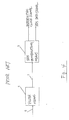
- FIG. 3 shows a schematic block diagram of a conventional RDS data demodulator.
- This conventional RDS data demodulator includes a filter means 4 and an RDS demodulating means 5.
- the filter means 4 extracts an RDS modulation signal 7 from an analog FM demodulation signal 6 which is demodulated by using the analog signal processing technique.
- the RDS modulation signal 7 is outputted from the filter means 4.
- the RDS demodulating means 5 demodulates this output signal from the filter means 4 to derive an RDS data signal and a reproduction clock signal used to demodulate the RDS data.
- the filter means 4 employs an analog filter such as a switched capacitor circuit. At the output terminal of this filter means 4, the RDS modulation signal 7 which has been separated from the speech (audio) signal is outputted. It should also be understood that when the RDS modulation signal and the ARI modulation signal are simultaneously broadcasted from the broadcast station, both the RDS modulation signal and the ARI modulation signal are outputted at the same time.
- the RDS demodulating means 5 contains a costas loop type PLL for demodulating the DSB signal.
- the costas loop type PLL includes multipliers 8 and 9, a phase comparator 10, a loop filter 11, and a VCO 12.
- This type of PLL circuit carries out synchronization even when there is no subcarrier. That is, a synchronization can be established when the subcarrier becomes 0 degree, or 90 degrees with respect to the VCO. Consequently, such a PLL circuit is suitable for demodulating an RDS modulation signal having no subcarrier.
- the RDS modulation signal which has been DSB-demodulated, is outputted as the synchronization-detection output 13. If both the RDS modulation signal and the ARI modulation signal are transmitted at the same time, such an RDS modulation signal, which has been DSB-demodulated, is outputted as the quadrature detection output 14. This is because when both the ARI modulation signal and the RDS modulation signal are transmitted at the same time, only the ARI modulation signal is synchronized since the modulation factor of the ARI modulation signal is higher than that of the RDS modulation signal. As a result, the RDS modulation signal having the quadrature-relationship with the ARI modulation signal is outputted as the quadrature modulation output 14.
- Japanese Unexamined Patent Publication No. 62-206929 discloses an improved method capable of switching the ARI modulation signal and the RDS modulation signal.
- an ARI signal detecting circuit 15 is provided to receive the synchronization-detection output 13 of the costas loop type PLL circuit for judging whether or not the ARI signal is present.
- a signal switching circuit 16 is employed to select between the synchronization-detection output 13 and the quadrature-detection output 14.
- the ARI signal detecting circuit 15 In response to a judgment result made by the ARI signal detecting circuit 15, either the synchronization-detection output 13 or the quadrature-detection output 14 is outputted from the signal switching circuit 16 to a post-stage circuit (not shown), so that the RDS signal which has been DSB demodulated is derived.
- this conventional circuit arrangement has the following problems.
- the RDS modulation signal and the ARI modulation signal are transmitted at the same time, the RDS signal cannot be derived until the ARI signal is detected by the ARI signal detecting circuit 15. Therefore, a lengthy time period is required to obtain the RDS data.
- the above-explained costas loop type PLL circuit would be locked to a third higher harmonic wave.
- This third higher harmonic wave is produced when the pilot signal having the frequency of 19 kHz and indicative of the stereophonic broadcasting program is distorted due to a multi-path phenomenon. Therefore, the ARI signal detecting circuit 15 erroneously detects an ARI signal. As a result, the signal switching circuit 16 makes the wrong selection in accordance with the wrong result from the ARI signal detecting circuit 15.
- the present invention is directed to a RDS data demodulator that substantially obviates one or more of the problems due to limitations and disadvantages of the related art.
- An object of the present invention is to provide an RDS data demodulator capable of attenuating an ARI signal in high precision without increasing a circuit size.
- Another object of the present invention is to provide an RDS data demodulator capable of acquiring RDS data continuously under stable condition irrespective of presence or absence of an ARI modulation signal.
- the RDS data demodulator of the present invention no longer uses the ARI signal detecting circuit and the signal switching circuit, which are employed in the conventional RDS data demodulator.
- an RDS data demodulator of the present invention includes an analog-to-digital converter for converting an analog FM signal into a digital FM modulation signal; a first filter to which the digital FM modulation signal is supplied, having a transfer zero point at a predetermined frequency, and for attenuating an information modulation signal; a second filter to which a filter output signal of the first filter is supplied, having a pass band characteristic at the predetermined frequency, and for extracting an RDS modulation signal; and RDS demodulating means for demodulating a filter output signal of the second filter so as to output both an RDS data signal and a reproduction clock signal used to demodulate the RDS data.
- a signal processing time period of the first filter is carried out at a frequency higher than that of a subcarrier of the RDS signal by four times; and a term "Z -1 " of the denominator of a transfer function of the first filter is equal to zero.
- a signal processing time period of the second filter instead of the first filter, is carried out at a frequency higher than that of a subcarrier of the RDS signal by four times; and a term "Z -1 " of the denominator of a transfer function of the second filter is equal to zero.
- the RDS data demodulator of the present invention operates as follows.
- an analog FM demodulation signal demodulated by way of an analog signal processing technique is converted into a digital FM demodulation signal 19 by an analog-to-digital (A/D) converter 18 for converting the analog FM demodulation signal into the corresponding digital FM demodulation signal.
- a signal 21 with an ARI modulation signal attenuated from the digital FM modulation signal 19 is produced from a first infinite impulse response type filter 20.
- This first infinite impulse response type filter 20 has a transmission zero point at a frequency of 57 kHz, and is capable of attenuating the ARI modulation signal.
- this signal 21 with the ARI modulation signal attenuated is inputted to a second infinite impulse response type filter 22.
- This second infinite impulse response type filter 22 has a pass band characteristic at a frequency of 57 kHz, and is capable of extracting an RDS modulation signal.
- the sufficiently attenuated ARI modulation signal is then supplied to the RDS demodulating circuit 24. Consequently, even when both the RDS modulation signal and the ARI modulation signal are transmitted at the same time, the ARI signal is no longer detected. Furthermore, the RDS modulation signal is no longer adversely influenced by the noise. As a result, the demodulated signal is more reliable.
- the infinite impulse response type filter since the infinite impulse response type filter is used, such a filter having a high quality factor Q is capable of attenuating only the ARI modulation signal. Moreover, the pass-band blocking frequency is not fluctuated due to the circuit elements used. Also, the circuit size is small.
- the signal processing time period of the first infinite impulse response type filter is selected so that its frequency is higher than that of the subcarrier of the RDS signal, the term "Z -1 " of the denominator in this transfer function can be made zero.
- the frequency of the transfer zero point can be made coincident with the subcarrier of the ARI modulation signal. Consequently, there are no quantization errors specific to a digital filter, the ARI signal can be attenuated in high precision, and also the hardware size can be reduced.
- the signal processing time period of the second infinite impulse response type filter is selected so that its frequency is higher than that of the subcarrier of the RDS signal, the term "Z -1 " of the denominator in this transfer function can be made zero. Accordingly, the frequency of the pass band can be made coincident with the subcarrier of the ARI modulation signal. As a result, there are no quantization errors specific to a digital filter, the RDS signal can pass through the second infinite impulse response type filter in high precision, and the associated hardware size can be reduced.
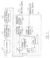
- Fig. 1 schematically illustrates a circuit arrangement of an RDS data demodulator according to a preferred embodiment of the present invention.
- an analog FM demodulation signal 17 is initially demodulated by using an analog signal processing technique, and then is converted into a digital FM demodulation signal 19 by an analog-to-digital (A/D) converter 18.
- A/D analog-to-digital
- the digital FM demodulation signal 19 is then provided to a first infinite impulse response type filter 20.
- the first infinite impulse response type filter 20 has a transmission zero point at a frequency of 57 kHz, and is provided mainly for attenuating the ARI modulation signal.
- the first infinite impulse response type filter 20 attenuates an ARI modulation signal in the digital FM modulation signal 19 and outputs a signal 21.
- the signal 21 is supplied to a second infinite impulse response type filter 22.
- the second infinite impulse response type filter 22 has a pass band characteristic at a frequency of 57 kHz, and is provided mainly for extracting an RDS modulation signal 23 from the signal 21.
- the RDS modulation signal 23 is outputted from the second infinite impulse response type filter 22 and supplied to an RDS demodulating circuit 24.
- the RDS modulation signal 23 contains the ARI modulation signal because the frequency bands of both are the same.
- the component of the ARI modulation signal has already been sufficiently attenuated at this point.
- the RDS demodulating circuit 24 demodulates the RDS demodulation signal 23 and supplies an RDS data signal 25 and a reproduction clock signal 26, which is used for demodulating the RDS data, to a post-stage circuit (not shown in figures). Since the operation of the RDS demodulating circuit 24 is similar to that of the conventional RDS demodulator, a detailed description thereof is omitted.
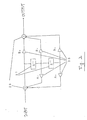
- Fig. 2 is a signal diagram of an infinite impulse response type filter used in the RDS data demodulator of the present invention.
- the infinite impulse response type filter includes delay circuits 27 for delaying an input signal by a time period corresponding to 1 sampling timing (1/F), coefficient multipliers 28 for multiplying the input signal by coefficients (A 1 , A 2 , B 0 , B 1 , B 2 ), and adders 29 for adding a plurality of inputs respectively to generate an output result.
- H BPF Z B ⁇ 1 - Z - 2 ) / ( 1 - A 1 ⁇ Z - 1 + A 2 ⁇ Z - 2
- H BEF B ⁇ 1 - Z - 2 ) / ( 1 - A 1 ⁇ Z - 1 - A 2 ⁇ Z - 2
- the first infinite impulse response type filter 20 is arranged based on the transfer function H BEF in formula (3), whereas the second infinite impulse response type filter 22 is arranged based on the transfer function H BPF in formula (2).
- the respective coefficients in formulae (2) and (3) have the following meanings.
- the coefficient "A 1 " is a factor for determining a pass-band blocking frequency, or a pass-band central frequency of the filter.
- the coefficient "A 2 " is a factor for determining a quality factor "Q" of the filter.
- the coefficient "B” denotes an element used to determine an amplification factor of input/output in a pass band.
- the filters based upon the transfer functions H BEF and H BPF of the above-described formulae (2) and (3) may be cascade-connected, if desired.
- the digital filter shown in Fig. 2 has a highly precise filtering characteristic, as compared with the conventional analog filters such as a switched capacitor circuit. This is because the calculations (namely, multiplication of coefficients) are carried out with digital processing operations and there is no fluctuation in the circuit elements. Consequently, such a digital filter is ideal to be used for attenuating the ARI modulation signal, and for extracting the RDS modulation signal. This also allows a small number of circuit elements to be used for performing these functions.
- a sampling period (1/F) is also a major factor for determining a filtering characteristic.
- the sampling frequency "F” is selected to be a frequency higher than 57 kHz (namely, the subcarrier of RDS modulation signal) by 4 times.
- the parameter "A 1 " in the transfer functions H BEF and H BPF defined by the formulae (2) and (3) is set to "0."
- the pass-band central frequency of the band pass type filter according to the transfer function H BPF of the formula (2) is selected to be 57 kHz, so that this central frequency is made coincident with the frequency of the subcarrier of the RDS modulation signal.
- the pass-band blocking frequency of the pass-band block (stop) type filter according to the transfer function H BEF of the formula (3) also becomes 57 kHz, which coincides with the frequency of the subcarrier of the ARI modulation signal.
- the parameter "A 1 " equals to "0” implies that the parameter "A 1 " is not adversely influenced by quantization errors. In other words, it implies that neither the pass-band blocking frequency of the digital filter according to the transfer function H BEF of the formula (3), nor the pass-band central frequency of the digital filter according to the transfer function H BEF of the formula (2) is adversely influenced by the quantization. Furthermore, the coefficient "0” implies that the output of the coefficient multiplier becomes "zero.” In other words, the coefficient multiplier is not required.
- the sampling period (1/F) is selected to be a frequency higher than that of the subcarrier of the RDS modulation by 4 times, the term "Z -1 " of the denominator of the transfer function for the resultant filter can be made zero.
- digital filters operable with high precisions can be formed by using a simple calculation, thus reducing the hardware scale of these digital filters.
- the ARI modulation signal can be precisely attenuated by the first infinite impulse response type filter 20 to a high degree so that the signal 21 from which the ARI modulation signal has been attenuated can be outputted.
- Both the attenuated ARI modulation signal and the RDS modulation signal are extracted from the second infinite impulse response type filter 22. Then, the extracted signals are supplied as the signal 23 to the RDS demodulating circuit 24.
- the costas loop PLL circuit 33 employed in the RDS demodulating circuit 24 is neither synchronized with the attenuated ARI modulation signal nor the high frequency signal of the pilot signal, but is synchronized with the RDS modulation signal.
- the DSB demodulation signal can be obtained as the synchronization-detection output 34 irrespective of presence or absence of the ARI modulation signal. Accordingly, the signal switching circuit employed in the conventional RDS demodulator is no longer required, which switches the synchronization-detection output 34 and the quadrature-detection output 35.
- the RDS data can be continuously supplied under stable conditions.
- the RDS modulation signal which has been DSB-demodulated is demodulated in the 2-phase PSK demodulating manner by the 2-phase PSK demodulating circuit 36.
- the reproduction clock signal 26 is outputted by the clock reproducing circuit 37.
- the signal demodulated in the 2-phase PSK demodulating manner is differential-decoded by the differential decoding circuit 38, and is outputted as the RDS data signal 25.
- the band block type filter is provided before the band pass type filter in the RDS data demodulator in accordance with the present invention. This is because the band block type filter has a high Q, and may be easily influenced by the group delay distortion adversely. Under such a circumstance, if the filter output of the band pass type filter, which is adversely influenced by the group delay distortion, were to be supplied to the band block type filter, the ARI signal components would not be sufficiently attenuated.
- both the ARI detecting circuit and the signal switching circuit which are required in the conventional RDS data demodulator, can be omitted.
- the digital filter used has a highly precise filtering characteristic as compared to the conventional analog filter such as a switched capacitor circuit, since the calculations (namely, multiplication of coefficients) are carried out in accordance with the digital processing operations. Therefore, there is no fluctuation in the circuit elements.
- the infinite impulse response type filter is used, the circuit size can be reduced.
- the signal processing time period of the infinite impulse response type filter is selected to be a frequency four times higher than that of the subcarrier of the RDS signal, the term "Z -1 " of the denominator in the transfer function can be made zero. Furthermore, either the frequency of the transfer zero point or the frequency of the pass band can be made coincident with either the RDS modulation signal or the subcarrier of the ARI modulation signal. As a result, there is no quantization error, which a digital filter normally has. Also, a target signal can be attenuated, or extracted in high precision. Moreover, the hardware size can be further reduced.
Claims (8)
- Démodulateur de données de système de radiocommunication de données (RDS) comprenant :un convertisseur analogique-numérique pour convertir un signal de démodulation FM analogique en signal de démodulation FM numérique ;un premier filtre ayant un point zéro de transfert à une fréquence prédéterminée, pour recevoir le signal de démodulation FM numérique et pour affaiblir un signal de modulation d'informations du signal de démodulation FM numérique ;un second filtre ayant une caractéristique de passe-bande à la fréquence prédéterminée, pour recevoir un signal de sortie de filtre du premier filtre et pour extraire un signal de modulation RDS ; etdes moyens de démodulation RDS pour démoduler le signal de modulation RDS du second filtre pour transmettre en sortie un signal de données RDS et un signal d'horloge de reproduction utilisé pour démoduler le signal RDS.
- Démodulateur de données RDS selon la revendication 1, dans lequel une période de traitement de signal du premier filtre est conduite à une fréquence quatre fois plus élevée qu'une fréquence de sous-porteuse du signal de données RDS.
- Démodulateur de données RDS selon la revendication 2, dans lequel le premier filtre a une fonction de transfert de HBEF(Z) = B(1+Z-2)/(1-A1Z-1-A2Z-2) et A1 est égal à zéro.
- Démodulateur de données RDS selon la revendication 1, dans lequel une période de traitement de signal du second filtre est conduite à une fréquence quatre fois plus élevée qu'une fréquence de sous-porteuse du signal de données RDS.
- Démodulateur de données RDS selon la revendication 4, dans lequel le second filtre a une fonction de transfert de HBPF(Z) = B(1-Z-2)/(1-A1Z-1-A2 Z-2) et A1 est égal à zéro.
- Démodulateur de données RDS selon la revendication 1, dans lequel le premier filtre est un filtre de type récursif.
- Démodulateur de données RDS selon la revendication 1, dans lequel le second filtre est un filtre de type récursif.
- Démodulateur dé données RDS selon la revendication 1, dans lequel la fréquence prédéterminée est de 57 kHz.
Applications Claiming Priority (2)
| Application Number | Priority Date | Filing Date | Title |
|---|---|---|---|
| JP6626298 | 1998-03-02 | ||
| JP06626298A JP3671111B2 (ja) | 1998-03-02 | 1998-03-02 | Rdsデータ復調器 |
Publications (3)
| Publication Number | Publication Date |
|---|---|
| EP0949772A2 EP0949772A2 (fr) | 1999-10-13 |
| EP0949772A3 EP0949772A3 (fr) | 2001-12-05 |
| EP0949772B1 true EP0949772B1 (fr) | 2007-09-05 |
Family
ID=13310775
Family Applications (1)
| Application Number | Title | Priority Date | Filing Date |
|---|---|---|---|
| EP99102846A Expired - Lifetime EP0949772B1 (fr) | 1998-03-02 | 1999-03-01 | Demodulateur des signaux RDS pour la réception de programmes de radiodiffusion comportant à la fois un signal RDS et un signal ARI, avec un dispositif de filtrage numérique assurant une attenuation élevée du signal ARI |
Country Status (4)
| Country | Link |
|---|---|
| US (1) | US6556631B1 (fr) |
| EP (1) | EP0949772B1 (fr) |
| JP (1) | JP3671111B2 (fr) |
| DE (1) | DE69937018T2 (fr) |
Families Citing this family (4)
| Publication number | Priority date | Publication date | Assignee | Title |
|---|---|---|---|---|
| DE10111590B4 (de) * | 2001-03-10 | 2004-05-06 | Harman Becker Automotive Systems (Becker Division) Gmbh | Verfahren und Schaltungsanordnung zur Demodulation des RDS-Signals |
| SE0104403D0 (sv) * | 2001-12-21 | 2001-12-21 | Bang & Olufsen Powerhouse As | Attenuation control for digital power converters |
| EP1432157B1 (fr) * | 2002-12-20 | 2007-09-19 | Sony Deutschland GmbH | Procédé d'extraction d'une composante de signal RDS et récepteur de signaux |
| US20050289447A1 (en) * | 2004-06-29 | 2005-12-29 | The Boeing Company | Systems and methods for generating and storing referential links in a database |
Family Cites Families (4)
| Publication number | Priority date | Publication date | Assignee | Title |
|---|---|---|---|---|
| JPS62206929A (ja) | 1986-03-06 | 1987-09-11 | Mitsubishi Electric Corp | ラジオデ−タ復調回路 |
| NL8802961A (nl) * | 1988-12-01 | 1990-07-02 | Philips Nv | Fm-ontvanger. |
| US5357574A (en) * | 1992-12-14 | 1994-10-18 | Ford Motor Company | Coherent signal generation in digital radio receiver |
| JP3132802B2 (ja) | 1995-09-06 | 2001-02-05 | シャープ株式会社 | Fm多重受信装置 |
-
1998
- 1998-03-02 JP JP06626298A patent/JP3671111B2/ja not_active Expired - Fee Related
-
1999
- 1999-03-01 DE DE69937018T patent/DE69937018T2/de not_active Expired - Lifetime
- 1999-03-01 US US09/259,286 patent/US6556631B1/en not_active Expired - Fee Related
- 1999-03-01 EP EP99102846A patent/EP0949772B1/fr not_active Expired - Lifetime
Also Published As
| Publication number | Publication date |
|---|---|
| JP3671111B2 (ja) | 2005-07-13 |
| EP0949772A3 (fr) | 2001-12-05 |
| DE69937018D1 (de) | 2007-10-18 |
| EP0949772A2 (fr) | 1999-10-13 |
| JPH11252032A (ja) | 1999-09-17 |
| US6556631B1 (en) | 2003-04-29 |
| DE69937018T2 (de) | 2008-06-26 |
Similar Documents
| Publication | Publication Date | Title |
|---|---|---|
| Taura et al. | A digital audio broadcasting (DAB) receiver | |
| US7787630B2 (en) | FM stereo decoder incorporating Costas loop pilot to stereo component phase correction | |
| US5483695A (en) | Intermediate frequency FM receiver using analog oversampling to increase signal bandwidth | |
| AU769846B2 (en) | Audio blend method, transmitter and receiver for AM and FM in band on channel digital audio broadcasting | |
| US5507024A (en) | FM data-system radio receiver | |
| EP0512606B1 (fr) | Stéréodécodeur discret dans le temps | |
| US6868129B2 (en) | Demodulator for a radio receiver and method of operation | |
| US6389270B1 (en) | Station scan method and apparatus for radio receivers | |
| US20040029548A1 (en) | Radio receiver having a variable bandwidth IF filter and method therefor | |
| EP0923272A2 (fr) | Mesure de la qualité du signal utilisant un detecteur MF full-complex | |
| JP3387537B2 (ja) | Rds受信機の2相psk復調回路 | |
| EP0949772B1 (fr) | Demodulateur des signaux RDS pour la réception de programmes de radiodiffusion comportant à la fois un signal RDS et un signal ARI, avec un dispositif de filtrage numérique assurant une attenuation élevée du signal ARI | |
| EP1158676A2 (fr) | Circuit pour la réduction d'interférences et récepteur de télévision | |
| EP1064765B1 (fr) | Selection et abaissement directs de frequence pour recepteurs numeriques | |
| KR20050036893A (ko) | 디지털 fm 스테레오 디코더 및 동작 방법 | |
| JP2001168745A (ja) | 情報再生方法及びラジオデータシステム信号復調装置 | |
| US4430747A (en) | Receiving apparatus for stereophonic broadcast having amplitude and angle modulated signal components | |
| EP0471412B1 (fr) | Récepteurs pour transmissions en modulation de fréquence | |
| WO1996013897A1 (fr) | Dispositif de telecommunications presentant une diminution de la sensibilite aux interferences dans un meme canal | |
| EP1061654B1 (fr) | Détection du bruit d'un signal audio de télédiffusion FM demodule en frequence | |
| JP2924198B2 (ja) | Cs放送受信機 | |
| EP0420584B1 (fr) | Circuit PLL démodulateur dans un récepteur d'informations de trafic | |
| JP4440050B2 (ja) | 受信装置 | |
| KR19990060510A (ko) | 디지털 잔류측파대 복조장치 | |
| US20050036626A1 (en) | Method and system for processing a Japanese BTSC signal |
Legal Events
| Date | Code | Title | Description |
|---|---|---|---|
| PUAI | Public reference made under article 153(3) epc to a published international application that has entered the european phase |
Free format text: ORIGINAL CODE: 0009012 |
|
| AK | Designated contracting states |
Kind code of ref document: A2 Designated state(s): AT BE CH CY DE DK ES FI FR GB GR IE IT LI LU MC NL PT SE Kind code of ref document: A2 Designated state(s): DE FR GB |
|
| AX | Request for extension of the european patent |
Free format text: AL;LT;LV;MK;RO;SI |
|
| PUAL | Search report despatched |
Free format text: ORIGINAL CODE: 0009013 |
|
| AK | Designated contracting states |
Kind code of ref document: A3 Designated state(s): AT BE CH CY DE DK ES FI FR GB GR IE IT LI LU MC NL PT SE |
|
| AX | Request for extension of the european patent |
Free format text: AL;LT;LV;MK;RO;SI |
|
| RIC1 | Information provided on ipc code assigned before grant |
Free format text: 7H 04H 1/00 A, 7H 03H 17/02 B, 7H 04B 1/16 B |
|
| 17P | Request for examination filed |
Effective date: 20011121 |
|
| AKX | Designation fees paid |
Free format text: DE FR GB |
|
| 17Q | First examination report despatched |
Effective date: 20040210 |
|
| GRAP | Despatch of communication of intention to grant a patent |
Free format text: ORIGINAL CODE: EPIDOSNIGR1 |
|
| GRAS | Grant fee paid |
Free format text: ORIGINAL CODE: EPIDOSNIGR3 |
|
| GRAA | (expected) grant |
Free format text: ORIGINAL CODE: 0009210 |
|
| AK | Designated contracting states |
Kind code of ref document: B1 Designated state(s): DE FR GB |
|
| REG | Reference to a national code |
Ref country code: GB Ref legal event code: FG4D |
|
| REF | Corresponds to: |
Ref document number: 69937018 Country of ref document: DE Date of ref document: 20071018 Kind code of ref document: P |
|
| REG | Reference to a national code |
Ref country code: GB Ref legal event code: 746 Effective date: 20080117 |
|
| ET | Fr: translation filed | ||
| PLBE | No opposition filed within time limit |
Free format text: ORIGINAL CODE: 0009261 |
|
| STAA | Information on the status of an ep patent application or granted ep patent |
Free format text: STATUS: NO OPPOSITION FILED WITHIN TIME LIMIT |
|
| 26N | No opposition filed |
Effective date: 20080606 |
|
| PGFP | Annual fee paid to national office [announced via postgrant information from national office to epo] |
Ref country code: FR Payment date: 20120319 Year of fee payment: 14 |
|
| PGFP | Annual fee paid to national office [announced via postgrant information from national office to epo] |
Ref country code: DE Payment date: 20120222 Year of fee payment: 14 |
|
| PGFP | Annual fee paid to national office [announced via postgrant information from national office to epo] |
Ref country code: GB Payment date: 20120301 Year of fee payment: 14 |
|
| GBPC | Gb: european patent ceased through non-payment of renewal fee |
Effective date: 20130301 |
|
| REG | Reference to a national code |
Ref country code: FR Ref legal event code: ST Effective date: 20131129 |
|
| REG | Reference to a national code |
Ref country code: DE Ref legal event code: R119 Ref document number: 69937018 Country of ref document: DE Effective date: 20131001 |
|
| PG25 | Lapsed in a contracting state [announced via postgrant information from national office to epo] |
Ref country code: DE Free format text: LAPSE BECAUSE OF NON-PAYMENT OF DUE FEES Effective date: 20131001 Ref country code: FR Free format text: LAPSE BECAUSE OF NON-PAYMENT OF DUE FEES Effective date: 20130402 Ref country code: GB Free format text: LAPSE BECAUSE OF NON-PAYMENT OF DUE FEES Effective date: 20130301 |