EP0777272B1 - Semiconductor device - Google Patents
Semiconductor device Download PDFInfo
- Publication number
- EP0777272B1 EP0777272B1 EP96114255A EP96114255A EP0777272B1 EP 0777272 B1 EP0777272 B1 EP 0777272B1 EP 96114255 A EP96114255 A EP 96114255A EP 96114255 A EP96114255 A EP 96114255A EP 0777272 B1 EP0777272 B1 EP 0777272B1
- Authority
- EP
- European Patent Office
- Prior art keywords
- region
- main surface
- heat sink
- semiconductor element
- grooves
- Prior art date
- Legal status (The legal status is an assumption and is not a legal conclusion. Google has not performed a legal analysis and makes no representation as to the accuracy of the status listed.)
- Expired - Lifetime
Links
Images


Classifications
-
- H—ELECTRICITY
- H01—ELECTRIC ELEMENTS
- H01L—SEMICONDUCTOR DEVICES NOT COVERED BY CLASS H10
- H01L23/00—Details of semiconductor or other solid state devices
- H01L23/48—Arrangements for conducting electric current to or from the solid state body in operation, e.g. leads, terminal arrangements ; Selection of materials therefor
- H01L23/488—Arrangements for conducting electric current to or from the solid state body in operation, e.g. leads, terminal arrangements ; Selection of materials therefor consisting of soldered or bonded constructions
- H01L23/495—Lead-frames or other flat leads
- H01L23/49575—Assemblies of semiconductor devices on lead frames
-
- H—ELECTRICITY
- H01—ELECTRIC ELEMENTS
- H01L—SEMICONDUCTOR DEVICES NOT COVERED BY CLASS H10
- H01L21/00—Processes or apparatus adapted for the manufacture or treatment of semiconductor or solid state devices or of parts thereof
- H01L21/02—Manufacture or treatment of semiconductor devices or of parts thereof
- H01L21/04—Manufacture or treatment of semiconductor devices or of parts thereof the devices having at least one potential-jump barrier or surface barrier, e.g. PN junction, depletion layer or carrier concentration layer
- H01L21/50—Assembly of semiconductor devices using processes or apparatus not provided for in a single one of the subgroups H01L21/06 - H01L21/326, e.g. sealing of a cap to a base of a container
- H01L21/56—Encapsulations, e.g. encapsulation layers, coatings
- H01L21/565—Moulds
-
- H—ELECTRICITY
- H01—ELECTRIC ELEMENTS
- H01L—SEMICONDUCTOR DEVICES NOT COVERED BY CLASS H10
- H01L23/00—Details of semiconductor or other solid state devices
- H01L23/34—Arrangements for cooling, heating, ventilating or temperature compensation ; Temperature sensing arrangements
- H01L23/42—Fillings or auxiliary members in containers or encapsulations selected or arranged to facilitate heating or cooling
- H01L23/433—Auxiliary members in containers characterised by their shape, e.g. pistons
- H01L23/4334—Auxiliary members in encapsulations
-
- H—ELECTRICITY
- H01—ELECTRIC ELEMENTS
- H01L—SEMICONDUCTOR DEVICES NOT COVERED BY CLASS H10
- H01L2224/00—Indexing scheme for arrangements for connecting or disconnecting semiconductor or solid-state bodies and methods related thereto as covered by H01L24/00
- H01L2224/01—Means for bonding being attached to, or being formed on, the surface to be connected, e.g. chip-to-package, die-attach, "first-level" interconnects; Manufacturing methods related thereto
- H01L2224/42—Wire connectors; Manufacturing methods related thereto
- H01L2224/44—Structure, shape, material or disposition of the wire connectors prior to the connecting process
- H01L2224/45—Structure, shape, material or disposition of the wire connectors prior to the connecting process of an individual wire connector
- H01L2224/45001—Core members of the connector
- H01L2224/45099—Material
- H01L2224/451—Material with a principal constituent of the material being a metal or a metalloid, e.g. boron (B), silicon (Si), germanium (Ge), arsenic (As), antimony (Sb), tellurium (Te) and polonium (Po), and alloys thereof
- H01L2224/45117—Material with a principal constituent of the material being a metal or a metalloid, e.g. boron (B), silicon (Si), germanium (Ge), arsenic (As), antimony (Sb), tellurium (Te) and polonium (Po), and alloys thereof the principal constituent melting at a temperature of greater than or equal to 400°C and less than 950°C
- H01L2224/45124—Aluminium (Al) as principal constituent
-
- H—ELECTRICITY
- H01—ELECTRIC ELEMENTS
- H01L—SEMICONDUCTOR DEVICES NOT COVERED BY CLASS H10
- H01L2224/00—Indexing scheme for arrangements for connecting or disconnecting semiconductor or solid-state bodies and methods related thereto as covered by H01L24/00
- H01L2224/01—Means for bonding being attached to, or being formed on, the surface to be connected, e.g. chip-to-package, die-attach, "first-level" interconnects; Manufacturing methods related thereto
- H01L2224/42—Wire connectors; Manufacturing methods related thereto
- H01L2224/44—Structure, shape, material or disposition of the wire connectors prior to the connecting process
- H01L2224/45—Structure, shape, material or disposition of the wire connectors prior to the connecting process of an individual wire connector
- H01L2224/45001—Core members of the connector
- H01L2224/45099—Material
- H01L2224/451—Material with a principal constituent of the material being a metal or a metalloid, e.g. boron (B), silicon (Si), germanium (Ge), arsenic (As), antimony (Sb), tellurium (Te) and polonium (Po), and alloys thereof
- H01L2224/45138—Material with a principal constituent of the material being a metal or a metalloid, e.g. boron (B), silicon (Si), germanium (Ge), arsenic (As), antimony (Sb), tellurium (Te) and polonium (Po), and alloys thereof the principal constituent melting at a temperature of greater than or equal to 950°C and less than 1550°C
- H01L2224/45144—Gold (Au) as principal constituent
-
- H—ELECTRICITY
- H01—ELECTRIC ELEMENTS
- H01L—SEMICONDUCTOR DEVICES NOT COVERED BY CLASS H10
- H01L2224/00—Indexing scheme for arrangements for connecting or disconnecting semiconductor or solid-state bodies and methods related thereto as covered by H01L24/00
- H01L2224/01—Means for bonding being attached to, or being formed on, the surface to be connected, e.g. chip-to-package, die-attach, "first-level" interconnects; Manufacturing methods related thereto
- H01L2224/42—Wire connectors; Manufacturing methods related thereto
- H01L2224/47—Structure, shape, material or disposition of the wire connectors after the connecting process
- H01L2224/48—Structure, shape, material or disposition of the wire connectors after the connecting process of an individual wire connector
- H01L2224/4805—Shape
- H01L2224/4809—Loop shape
- H01L2224/48091—Arched
-
- H—ELECTRICITY
- H01—ELECTRIC ELEMENTS
- H01L—SEMICONDUCTOR DEVICES NOT COVERED BY CLASS H10
- H01L2224/00—Indexing scheme for arrangements for connecting or disconnecting semiconductor or solid-state bodies and methods related thereto as covered by H01L24/00
- H01L2224/01—Means for bonding being attached to, or being formed on, the surface to be connected, e.g. chip-to-package, die-attach, "first-level" interconnects; Manufacturing methods related thereto
- H01L2224/42—Wire connectors; Manufacturing methods related thereto
- H01L2224/47—Structure, shape, material or disposition of the wire connectors after the connecting process
- H01L2224/48—Structure, shape, material or disposition of the wire connectors after the connecting process of an individual wire connector
- H01L2224/481—Disposition
- H01L2224/48151—Connecting between a semiconductor or solid-state body and an item not being a semiconductor or solid-state body, e.g. chip-to-substrate, chip-to-passive
- H01L2224/48221—Connecting between a semiconductor or solid-state body and an item not being a semiconductor or solid-state body, e.g. chip-to-substrate, chip-to-passive the body and the item being stacked
- H01L2224/48245—Connecting between a semiconductor or solid-state body and an item not being a semiconductor or solid-state body, e.g. chip-to-substrate, chip-to-passive the body and the item being stacked the item being metallic
- H01L2224/48247—Connecting between a semiconductor or solid-state body and an item not being a semiconductor or solid-state body, e.g. chip-to-substrate, chip-to-passive the body and the item being stacked the item being metallic connecting the wire to a bond pad of the item
-
- H—ELECTRICITY
- H01—ELECTRIC ELEMENTS
- H01L—SEMICONDUCTOR DEVICES NOT COVERED BY CLASS H10
- H01L24/00—Arrangements for connecting or disconnecting semiconductor or solid-state bodies; Methods or apparatus related thereto
- H01L24/01—Means for bonding being attached to, or being formed on, the surface to be connected, e.g. chip-to-package, die-attach, "first-level" interconnects; Manufacturing methods related thereto
- H01L24/42—Wire connectors; Manufacturing methods related thereto
- H01L24/44—Structure, shape, material or disposition of the wire connectors prior to the connecting process
- H01L24/45—Structure, shape, material or disposition of the wire connectors prior to the connecting process of an individual wire connector
-
- H—ELECTRICITY
- H01—ELECTRIC ELEMENTS
- H01L—SEMICONDUCTOR DEVICES NOT COVERED BY CLASS H10
- H01L24/00—Arrangements for connecting or disconnecting semiconductor or solid-state bodies; Methods or apparatus related thereto
- H01L24/01—Means for bonding being attached to, or being formed on, the surface to be connected, e.g. chip-to-package, die-attach, "first-level" interconnects; Manufacturing methods related thereto
- H01L24/42—Wire connectors; Manufacturing methods related thereto
- H01L24/47—Structure, shape, material or disposition of the wire connectors after the connecting process
- H01L24/48—Structure, shape, material or disposition of the wire connectors after the connecting process of an individual wire connector
-
- H—ELECTRICITY
- H01—ELECTRIC ELEMENTS
- H01L—SEMICONDUCTOR DEVICES NOT COVERED BY CLASS H10
- H01L2924/00—Indexing scheme for arrangements or methods for connecting or disconnecting semiconductor or solid-state bodies as covered by H01L24/00
- H01L2924/0001—Technical content checked by a classifier
- H01L2924/00014—Technical content checked by a classifier the subject-matter covered by the group, the symbol of which is combined with the symbol of this group, being disclosed without further technical details
-
- H—ELECTRICITY
- H01—ELECTRIC ELEMENTS
- H01L—SEMICONDUCTOR DEVICES NOT COVERED BY CLASS H10
- H01L2924/00—Indexing scheme for arrangements or methods for connecting or disconnecting semiconductor or solid-state bodies as covered by H01L24/00
- H01L2924/01—Chemical elements
- H01L2924/01079—Gold [Au]
-
- H—ELECTRICITY
- H01—ELECTRIC ELEMENTS
- H01L—SEMICONDUCTOR DEVICES NOT COVERED BY CLASS H10
- H01L2924/00—Indexing scheme for arrangements or methods for connecting or disconnecting semiconductor or solid-state bodies as covered by H01L24/00
- H01L2924/10—Details of semiconductor or other solid state devices to be connected
- H01L2924/11—Device type
- H01L2924/13—Discrete devices, e.g. 3 terminal devices
- H01L2924/1304—Transistor
- H01L2924/1305—Bipolar Junction Transistor [BJT]
- H01L2924/13055—Insulated gate bipolar transistor [IGBT]
-
- H—ELECTRICITY
- H01—ELECTRIC ELEMENTS
- H01L—SEMICONDUCTOR DEVICES NOT COVERED BY CLASS H10
- H01L2924/00—Indexing scheme for arrangements or methods for connecting or disconnecting semiconductor or solid-state bodies as covered by H01L24/00
- H01L2924/10—Details of semiconductor or other solid state devices to be connected
- H01L2924/11—Device type
- H01L2924/14—Integrated circuits
-
- H—ELECTRICITY
- H01—ELECTRIC ELEMENTS
- H01L—SEMICONDUCTOR DEVICES NOT COVERED BY CLASS H10
- H01L2924/00—Indexing scheme for arrangements or methods for connecting or disconnecting semiconductor or solid-state bodies as covered by H01L24/00
- H01L2924/15—Details of package parts other than the semiconductor or other solid state devices to be connected
- H01L2924/151—Die mounting substrate
- H01L2924/153—Connection portion
- H01L2924/1532—Connection portion the connection portion being formed on the die mounting surface of the substrate
-
- H—ELECTRICITY
- H01—ELECTRIC ELEMENTS
- H01L—SEMICONDUCTOR DEVICES NOT COVERED BY CLASS H10
- H01L2924/00—Indexing scheme for arrangements or methods for connecting or disconnecting semiconductor or solid-state bodies as covered by H01L24/00
- H01L2924/15—Details of package parts other than the semiconductor or other solid state devices to be connected
- H01L2924/151—Die mounting substrate
- H01L2924/156—Material
- H01L2924/157—Material with a principal constituent of the material being a metal or a metalloid, e.g. boron [B], silicon [Si], germanium [Ge], arsenic [As], antimony [Sb], tellurium [Te] and polonium [Po], and alloys thereof
- H01L2924/15738—Material with a principal constituent of the material being a metal or a metalloid, e.g. boron [B], silicon [Si], germanium [Ge], arsenic [As], antimony [Sb], tellurium [Te] and polonium [Po], and alloys thereof the principal constituent melting at a temperature of greater than or equal to 950 C and less than 1550 C
- H01L2924/15747—Copper [Cu] as principal constituent
-
- H—ELECTRICITY
- H01—ELECTRIC ELEMENTS
- H01L—SEMICONDUCTOR DEVICES NOT COVERED BY CLASS H10
- H01L2924/00—Indexing scheme for arrangements or methods for connecting or disconnecting semiconductor or solid-state bodies as covered by H01L24/00
- H01L2924/15—Details of package parts other than the semiconductor or other solid state devices to be connected
- H01L2924/181—Encapsulation
Definitions
- the present invention relates to a semiconductor device with a lead frame, a power semiconductor element provided thereon and a heat sink for heat radiation sealed with a resin, and particularly to an improvement for enhancing the heat radiating efficiency while maintaining the close contact between the heat sink and the resin.
- the invention relates to a semiconductor device according to the preamble of claim 1. Such a device is known from the document JP-A-60-170248 .
- Fig.13 is a front sectional view showing the inside structure of a conventional semiconductor device as background of the present invention.
- an IGBT element 11 as a power semiconductor element and controlling semiconductor elements 16 for controlling operation of the IGBT element 11 are affixed on the element mounting surface of a lead frame 3 made of copper.
- an aluminum heat sink 50 faces the main surface of the lead frame 3 on the opposite side to the element mounting surface.
- the lead frame 3 and the heat sink 50, including the various elements mounted on the element mounting surface of the lead frame 3, are encapsulated with the electrically insulating sealing resin 2. This fixedly couples the heat sink 50 and the lead frame 3 and also protects the lead frame 3 and the various elements mounted thereon from external moisture etc.
- a small gap is provided between the lead frame 3 and the heat sink 50, which is filled with the sealing resin 2. This provides high electric insulation and good heat conductivity between the lead frame 3 and the heat sink 50.
- the bottom of the heat sink 50 is exposed to the outside, and to this exposed surface an external radiation fin, or the like is connected to radiate the loss heat generated in the IGBT element 11 to the outside through the heat sink 50.
- Fig.14 is an overall perspective view of the heat sink 50.
- a plurality of grooves 20 parallel to one another are formed almost all over the top main surface of the heat sink 50, i.e., the main surface facing the lead frame 3, across its one edge to the other. These grooves 20 serve to enhance the close contact between the sealing resin 2 and the heat sink 50 and also to enhance the fluidity of the sealing resin 2 in the process of filling with the sealing resin 2 when manufacturing the device 150.
- the sealing resin 2 is interposed extra thick corresponding to the depth of the grooves 20 between the IGBT element 11 and the heat sink 50. This is a factor which increases the thermal resistance in the path of the loss heat generated in the IGBT element 11 to the heat sink 50. That is to say, the conventional device 150 sacrifices the radiating efficiency of the loss heat to improve the close contact between the sealing resin 2 and the heat sink 50 and to improve the fluidity of the sealing resin 2.
- this object is solved by a semiconductor device as defined in the main claim.
- Advantageous further developments of the semiconductor device according to the invention are specified in the sub-claims.
- a first aspect of the present invention is directed to a semiconductor device which comprises: a lead frame being like a sheet and electrically well conducting, the lead frame having one side main surface and another side main surface; a power semiconductor element fixed on the one side main surface; a heat sink being thermally well conducting and having one main surface, the one main surface being provided to face the other side main surface with a gap; and a sealing resin which is electrically insulating and fills the gap to couple the lead frame and the heat sink to each other while maintaining electric insulation from each other and seals the power semiconductor element; wherein a first region and a second region which is a remaining region other than the first region are defined in the one main surface of the heat sink; wherein the first region is flat in its entire region and a groove is formed in the second region; and wherein the power semiconductor element is disposed on the one side main surface selectively in a region covering the first region, and the groove is provided as being separated into a plurality of unit grooves, and the transverse sectional form of the respective grooves is rectangular or has
- the semiconductor device is characterized in that the first region is zonaly defined in a position which divides the one main surface of the heat sink into two, in that the second region is defined so that it is divided into zones on both sides of the first region, in that the plurality of unit grooves is disposed on both sides in the divided second region, and in that the one direction is a direction perpendicular to an elongate direction of the zonal first region.
- the semiconductor device further comprises a controlling semiconductor element for controlling the power semiconductor element, the controlling semiconductor element being fixed on the one side main surface selectively in a region covering the second region , and the sealing resin seals the controlling semiconductor element, too.
- an end on the first region side of each of the plurality of unit grooves is formed in a surface smoothly connecting a surface of the first region and a bottom of the each.
- the power semiconductor element disposed above the first region which is a flat region in the one main surface of the heat sink allows efficient transmission of loss heat generated in the power semiconductor element to the heat sink.
- the grooves formed in the second region which is a partial region of the one main surface of the heat sink enables excellent close contact between the heat sink and the sealing resin. That is to say, high heat radiating characteristic is obtained while maintaining close contact.
- the device of the second aspect since it has a controlling semiconductor element controlling the power semiconductor element, the device can be handled easily. Furthermore, since the power semiconductor element and the controlling semiconductor element are respectively disposed being separated above the first region and above the second region, the area of the first region can be reduced without deteriorating the heat radiating efficiency of loss heat of the power semiconductor element and the second region where the groove is formed can be enlarged to the maximum.
- the groove is separated into a plurality of unit grooves.
- a plurality of grooves (unit grooves) are formed in the second region, the close contact between the sealing resin and the heat sink is still better.
- the fluidity of the resin flowing in the gap between the lead frame and the heat sink is excellent in the process of sealing with the resin.
- each of the plurality of unit grooves since at least one end of each of the plurality of unit grooves reaches the edge of the one main surface of the heat sink, the fluidity of the resin flowing in the gap between the lead frame and the heat sink is still better in the process of sealing the resin.
- the first region is zonally defined in a position which divides the one main surface of the heat sink into two, mechanical strength of the heat sink is excellent. Furthermore, since the plurality of unit grooves are separated on both sides of the zonal first region and the unit grooves extend in the direction perpendicular to the elongate direction of the first region, the fluidity of the resin flowing in the gap between the lead frame and the heat sink is still better in the process of sealing with the resin. Particularly, it produces the effect that the resin smoothly flows in the narrowest interval between the first region and the lead frame.
- the fluidity of the resin flowing in the gap between the lead frame and the heat sink is still better in the process of sealing with the resin.
- the rectangular transverse sectional form of the groove allows still better close contact between the heat sink and the sealing resin.
- FIG.2 is a circuit diagram showing the circuit structure of a semiconductor device according to the first preferred embodiment.
- a device 101 includes a power circuit 10 having a power semiconductor element modulation-controlling the flow of the main current charged with supply of power to a load and a control circuit 15 controlling operation of the power semiconductor element.
- the power circuit 10 includes an IGBT element 11 as a power semiconductor element and a free wheel diode 12.
- the IGBT element 11 conducts and cuts off (i.e., switches) the main current flowing from the collector electrode C to the emitter electrode E in response to the gate voltage signal inputted to the gate electrode G. This main current is supplied to an external load through the external terminals 5 connected to the collector electrode C and the emitter electrode E.
- the free wheel diode 12 connected to the IGBT element 11 in the inverse-parallel connection serves to prevent application of excessive reverse current to the IGBT element 11.
- the control circuit 15 connected to the power circuit 10 through a plurality of interconnections 14 includes the controlling semiconductor element 16 as an integrated circuit element playing the main role in controlling the IGBT element 11, with a resistance element 17, a capacitance element 18, etc. These elements form a driving circuit and a protection circuit.
- the driving circuit is a circuit portion in the control circuit for transmitting the gate voltage signal to the gate electrode G in response to the control signal inputted to one of the plurality of external terminals 6.
- the protection circuit is a circuit portion for monitoring the operational environment of the IGBT element 11 to prevent damage to the IGBT element 11 when an abnormality occurs.
- the protection circuit shown in Fig.2 monitors the voltage between the collector electrode C and the emitter electrode E, i.e., the collector-emitter voltage and, when the voltage becomes too large above a certain reference value, it drives the gate electrode G to cut off the IGBT element 11 irrespective of the external control signal.
- the protection circuit also monitors the weak current flowing in the sense electrode S in proportion to the main current flowing in the IGBT element 11, i.e., the sense current, and when the main current becomes too large above a certain reference value, it drives the gate electrode G to cut off the IGBT element 11 irrespective of the external control signal.
- the protection circuit of Fig.2 transmits a signal indicating the occurrence of the abnormality to the outside through the external terminals 6. This way, the protection circuit serves to protect the IGBT element 11 from damage caused by an abnormality such as an excessive voltage and an excessive current, for example.
- Fig.3 is a front sectional view of the device 101.
- various elements included in the control circuit 15 and the power circuit 10 are soldered in a plurality of portions on the sheet-like lead frame 3 substantially formed of metal with good electric conductivity, such as copper.
- Fig.3 shows the IGBT element 11 and the controlling semiconductor element 16 as representatives of these elements. These elements are preferably formed as bare chip elements as shown in Fig.3 .
- the IGBT element 11 and other portions of the lead frame 3 are electrically connected through the aluminum bonding wires 13, for example.
- the controlling semiconductor element 16 and still other portions of the lead frame 3 are electrically connected by the gold bonding wires 19, for example.
- the lead frame 3 forms the interconnection pattern 4 of the control circuit 15 and the power circuit 10 including the interconnection 14 and also forms the external terminal 6 and the external terminal 5.
- the plate-like heat sink 51 substantially composed of well heat conducting metal such as aluminum or copper, for example, is provided to face the bottom main surface of the lead frame 3 on the opposite side of the top main surface on which the various elements are mounted (the element mounting surface).
- the sealing resin 2 with an electric insulating property and good thermal conductivity seals up the part of the lead frame 3 corresponding to the interconnection pattern 4, the various elements mounted on the interconnection pattern 4 and the heat sink 51.
- a small gap is provided between the lead frame 3 and the heat sink 51, which is filled with the sealing resin 2.
- the sealing resin 2 put in the gap serves to electrically insulate the lead frame 3 and the heat sink 51 and also to well transmit the loss heat generated in the IGBT element 11 from the lead frame 3 to the heat sink 51.
- the sealing resin 2 also functions to fixedly couple the lead frame 3 and the heat sink 51 and to protect the interconnection pattern 4 and the various elements thereon from the external moisture and the like.
- Fig.4 is a bottom view of the device 101.
- Fig.3 described above corresponds to the section taken along the A-A line in Fig.4 .
- the external terminals 5 and the external terminals 6 protrude to the outside from the side walls of the sealing resin 2, and the bottom main surface of the heat sink, or its main surface on the side opposite to the top main surface facing the lead frame 3, is exposed in the bottom.
- an external heat radiation fin or the like (not shown) is connected to the device 101 so as to keep the thermal contact with the exposed surface of the heat sink 51, or its bottom main surface. This allows the loss heat generated in the IGBT element 11 to be efficiently radiated to the outside through the heat sink 51.
- the sealing resin 2 is provided with a pair of through holes 99 to enable easy connection of the radiation fin etc. with screws.
- Fig.1 is a perspective view of the heat sink 51.
- Fig.5 is a sectional view of the heat sink 51 taken along the line B-B in Fig.1 .
- the heat sink 51 has a plurality of grooves 21 parallel to one another formed on its top main surface.
- the grooves 21 are selectively formed on both sides of the center region 22 zonally extending from one end to the other end in such a position as divides the top main surface of the heat sink 51 into two, which is characteristically different from the heat sink 50 of the conventional device 150.
- all the grooves 21 are formed extending in the one direction perpendicular to the elongate direction of the zonal center region 22.
- Fig. 6 is an element arrangement diagram showing it, which shows the elements and the heat sink 51 in overlap.
- the device 101 has a plurality of sets of the power circuit 10 and the control circuit 15. (Six sets in the example of Fig.6 .)
- the IGBT element 11 and the free wheel diode 12 forming the power circuit 10, i.e., the heat generating elements, are arranged above the center region (first region) 22.
- the elements forming the control circuit 15, i.e., the elements generating almost no heat, are arranged above a both side region (second region) 23 defined separately in the both sides of the center region 22 in which the grooves 21 are arranged.
- Fig.6 shows the controlling semiconductor elements 16 as representatives of elements forming the control circuits 15.
- the thermal resistance between the lead frame 3 and the both side region 23 is as high as that in the conventional device 150.
- the thermal resistance between the lead frame 3 and the center region 22 is low enough.
- the heat generating elements and the elements generating almost no heat are separated in the center region 22 with no grooves 21 and in the both side region 23 with the grooves 21, respectively. This considerably increases the radiation efficiency of the loss heat generated from the heat generating elements such as the IGBT element 11 as compared with the conventional device 150. Especially, since the center region 22 in which the heat generating elements are disposed is positioned in the two-dividing center of the top main surface of the heat sink 51, the loss heat is liable to diffuse all over the heat sink 51, which also contributes to the increase in radiation efficiency.
- the region occupied by the heat generating elements such as the IGBT element 11 is sufficiently small as compared with the entire top main surface of the heat sink 51, so that the region in which the grooves 21 are disposed, though which is limited to the regions 23 smaller than that in the conventional device 150, covers most part of the top main surface of the heat sink 51. Accordingly, the contact performance between the sealing resin 2 and the heat sink 51 is not inferior to the conventional device 150. That is to say, the device 101 of this preferred embodiment achieves improvement of radiation efficiency while maintaining the close contact between the sealing resin 2 and the heat sink 51.
- the heat sink 51 has the advantage that it has excellent mechanical strength as compared with the heat sink 50 of the conventional device in which the grooves are formed almost all over the top main surface.
- Fig.7 is a sectional view of the heat sink 51 taken along the line C-C in Fig.1 , which shows the transverse sectional form of the grooves 21.
- the transverse section of the grooves 21 is rectangular in the heat sink 51 of the device 101. Accordingly, the close contact between the sealing resin 2 and the heat sink 51 is especially excellent.
- the grooves 21 may be "U-shaped", to produce corresponding effects.
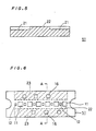
- Fig.8 is a process diagram showing this.
- FIG.8 shows the second step of the sealing process.
- the device in which the lead frame 3 and the various elements thereon have been sealed with the first sealing resin 40 is further sealed with the second sealing resin 41.
- the second step of sealing is carried out using the upper mold 34 having the cavity 35 and the lower mold 31 having the cavity 32.
- the heat sink 51 is placed on the bottom of the cavity 32.
- the liquid sealing resin 41 is injected through the injection path 33, heated and hardened to complete the sealing with the sealing resin 41.
- the sealing resin 41 fills the gap between the lead frame 3 and the heat sink 51 to couple them to each other, and preferably, it also covers the surface of the sealing resin 40 as shown in Fig.8 . This prevents peeling in the connection between the sealing resin 40 and the sealing resin 41, or invasion of water etc. from the connection to the inside.
- the sealing resin 41 flows in the narrow gap between the lower main surface of the lead frame 3 and the upper main surface of the heat sink 51. Since the plurality of grooves 21 are formed in the top main surface of the heat sink 51, which are all formed along one direction, setting the direction of the device as an object of sealing so that the opening of the injection path usually provided in one position is directed in the elongate direction (the one direction stated above) of the grooves 21 smoothens the flow of the sealing resin 41 in the gap.
- the sealing resin 41 flowing in the grooves 21 flows in the gap between the center region 22 and the lead frame 3.
- the fluidity is excellent in the narrowest interval between the center region 22 and the lead frame 3.
- the excellent fluidity of the sealing resin 41 in the gap between the heat sink 51 and the lead frame 3 prevents formation of voids in this gap and a certain breakdown voltage is stably obtained. That is to say, this results in the advantage of high reliability of the device.
- the device 101 in addition to the close contact between the heat sink 51 and the sealing resin 2 (41), the device 101 has the advantage that the heat radiation characteristic is improved while maintaining the high fluidity of the sealing resin 2 (41) in the sealing process.
- a material for the second sealing resin 41 which is for filling the gap between the lead frame 3 and the heat sink 51
- a material with especially excellent thermal conductivity as compared with the sealing resin 40 is selected as the material, such as an epoxy resin with fillers of silicon nitride mixed therein, for example.
- an ordinary epoxy resin at relatively low price is used as the sealing resin 40.
- the first sealing resin 40 provides stiffness to the lead frame 3 in advance, which facilitates precise adjustment of the gap between the lead frame 3 and the heat sink 51 to be filled with the sealing resin 41.
- the device 101 of the first preferred embodiment is especially suitable for production with the two-step sealing.
- the zonal region where grooves 21 are not formed in the top main surface of the heat sink 51 is placed in the position dividing the top main surface into two as the center region 22, as shown in Fig.1 .
- this zonal region may be shifted from the two-dividing position.
- the heat generating elements such as the IGBT element 11 etc. are located in the zonal region and other elements are located in the region where the grooves are formed.
- a device configured this way also improves the close contact between the heat sink 51 and the sealing resin 2 while maintaining the heat radiation efficiency high and also improves the fluidity of the sealing resin 2 (41) in the sealing process. Also, mechanical strength of the heat sink 51 will be fairly high.
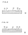
- the ends on the center region 22 side of the grooves 24 formed in the region 23 on both sides of the center region 22 are formed in a plane inclined at an obtuse angle with respect to the surface of the center region 22. This further improves the fluidity of the sealing resin 41 flowing on the top main surface of the heat sink 52 in the process of sealing with the sealing resin 41 ( Fig.8 ).
- the ends on the center region 22 side of the grooves 25 formed in both side region 23 are formed in a concave surface. Accordingly, similarly to the heat sink 52, the fluidity of the sealing resin 41 flowing on the top main surface of the heat sink 53 is further improved in the process of sealing with the sealing resin 41.
- ends of the grooves on the center region 22 side formed in such shape as smoothly connects the surface of the center region 22 and the bottom of the grooves provide high fluidity to the sealing resin 41 flowing on the top main surface of the heat sink as in the heat sinks 52 and 53.
- the transverse section of the grooves 26 formed in the both side region 23 are "V-shaped". This provides the advantage that the process of forming the grooves 26 by press processing is especially easy.
- Fig.12 is a plan view of a heat sink in a semiconductor device according to a third preferred embodiment, which shows elements and the heat sink in overlap.
- the device shown in Fig.12 is provided with two sets of the power circuit 10 and the control circuit 15.
- the heat sink 55 of this device has a plurality of grooves 27 formed along one direction, at least one end thereof reaching the edge of the top main surface of the heat sink 55. Accordingly, like the heat sink 51 etc., this provides good fluidity of the sealing resin.
- the IGBT element 11 and the free wheel diode 12 forming the power circuit 10 are disposed in positions out of the center region which divides the top main surface of the heat sink 55 into two.
- the grooves 27 are not formed in the region where these heat generating elements are disposed, but they are selectively formed in the other region.
- the elements forming the control circuit 15 such as the controlling semiconductor element 16 are disposed in the region where the grooves 27 are formed.
- the heat sink 55 structured this way also produces the effect of improving the heat radiating efficiency while maintaining the close contact between the heat sink 55 and the sealing resin 2 in the same way as the devices of the first preferred embodiment and so forth. That is to say, as exemplified in this preferred embodiment, even if the grooves are not formed in the region 23 ( Fig.6 ) on both sides of the center region 22 which divides the top main surface of the heat sink into two, if generally the grooves are selectively formed in the region where heat generating elements are not disposed in the top main surface of the heat sink, it produces the effect of compatibly improving the close contact of the sealing resin and the heat radiating efficiency.
Applications Claiming Priority (3)
| Application Number | Priority Date | Filing Date | Title |
|---|---|---|---|
| JP31255695 | 1995-11-30 | ||
| JP31255695A JP3345241B2 (ja) | 1995-11-30 | 1995-11-30 | 半導体装置 |
| JP312556/95 | 1995-11-30 |
Publications (3)
| Publication Number | Publication Date |
|---|---|
| EP0777272A2 EP0777272A2 (en) | 1997-06-04 |
| EP0777272A3 EP0777272A3 (en) | 2000-03-01 |
| EP0777272B1 true EP0777272B1 (en) | 2009-05-27 |
Family
ID=18030640
Family Applications (1)
| Application Number | Title | Priority Date | Filing Date |
|---|---|---|---|
| EP96114255A Expired - Lifetime EP0777272B1 (en) | 1995-11-30 | 1996-09-05 | Semiconductor device |
Country Status (4)
| Country | Link |
|---|---|
| US (1) | US5814878A (ja) |
| EP (1) | EP0777272B1 (ja) |
| JP (1) | JP3345241B2 (ja) |
| DE (1) | DE69637939D1 (ja) |
Families Citing this family (22)
| Publication number | Priority date | Publication date | Assignee | Title |
|---|---|---|---|---|
| JP3062691B1 (ja) * | 1999-02-26 | 2000-07-12 | 株式会社三井ハイテック | 半導体装置 |
| JP3581268B2 (ja) * | 1999-03-05 | 2004-10-27 | 株式会社東芝 | ヒートシンク付半導体装置およびその製造方法 |
| US6188130B1 (en) | 1999-06-14 | 2001-02-13 | Advanced Technology Interconnect Incorporated | Exposed heat spreader with seal ring |
| WO2002056378A1 (en) * | 2001-01-11 | 2002-07-18 | Matsushita Electric Industrial Co., Ltd. | Circuit board and production method therefor |
| JP4286465B2 (ja) | 2001-02-09 | 2009-07-01 | 三菱電機株式会社 | 半導体装置とその製造方法 |
| US7061080B2 (en) * | 2001-06-11 | 2006-06-13 | Fairchild Korea Semiconductor Ltd. | Power module package having improved heat dissipating capability |
| KR100723454B1 (ko) * | 2004-08-21 | 2007-05-30 | 페어차일드코리아반도체 주식회사 | 높은 열 방출 능력을 구비한 전력용 모듈 패키지 및 그제조방법 |
| JP2003100986A (ja) * | 2001-09-26 | 2003-04-04 | Toshiba Corp | 半導体装置 |
| JP2004357384A (ja) * | 2003-05-28 | 2004-12-16 | Toyoda Mach Works Ltd | ヒートシンクへのスイッチング素子取付構造 |
| US8269338B2 (en) * | 2006-08-10 | 2012-09-18 | Vishay General Semiconductor Llc | Semiconductor device having improved heat dissipation capabilities |
| JP5252819B2 (ja) * | 2007-03-26 | 2013-07-31 | 三菱電機株式会社 | 半導体装置およびその製造方法 |
| JP5124329B2 (ja) * | 2008-03-26 | 2013-01-23 | 新電元工業株式会社 | 半導体装置 |
| DE102009046172A1 (de) * | 2009-10-29 | 2011-05-05 | Robert Bosch Gmbh | Kühlkörper mit verbesserter Kühleffizienz, mit Kühlkörper ausgestattete Schaltung und Herstellungsverfahren hierfür |
| JP5649142B2 (ja) | 2011-04-05 | 2015-01-07 | パナソニック株式会社 | 封止型半導体装置及びその製造方法 |
| JP5857468B2 (ja) * | 2011-06-22 | 2016-02-10 | 株式会社デンソー | 半導体装置 |
| JP2013070026A (ja) | 2011-09-08 | 2013-04-18 | Rohm Co Ltd | 半導体装置、半導体装置の製造方法、半導体装置の実装構造、およびパワー用半導体装置 |
| JP2017055146A (ja) * | 2011-09-08 | 2017-03-16 | ローム株式会社 | 半導体装置、半導体装置の製造方法、半導体装置の実装構造、およびパワー用半導体装置 |
| JP5797126B2 (ja) * | 2012-02-06 | 2015-10-21 | 三菱電機株式会社 | 半導体装置 |
| CN107078067A (zh) | 2015-03-30 | 2017-08-18 | 瑞萨电子株式会社 | 半导体装置及其制造方法 |
| JP6824913B2 (ja) * | 2016-02-09 | 2021-02-03 | 三菱電機株式会社 | 電力用半導体装置及びその製造方法 |
| JP7134131B2 (ja) * | 2019-04-26 | 2022-09-09 | 三菱電機株式会社 | 半導体装置 |
| JPWO2023203754A1 (ja) * | 2022-04-22 | 2023-10-26 |
Family Cites Families (22)
| Publication number | Priority date | Publication date | Assignee | Title |
|---|---|---|---|---|
| JPS56147453A (en) * | 1980-04-17 | 1981-11-16 | Nec Corp | Semiconductor device |
| US4451973A (en) * | 1981-04-28 | 1984-06-05 | Matsushita Electronics Corporation | Method for manufacturing a plastic encapsulated semiconductor device and a lead frame therefor |
| DE3232632A1 (de) * | 1981-09-03 | 1983-03-10 | General Electric Co., Schenectady, N.Y. | Hochdruck-alkalimetalldampflampe mit verbesserter wirksamkeit |
| JPS60170248A (ja) * | 1984-02-15 | 1985-09-03 | Toshiba Corp | 半導体装置 |
| DE3684184D1 (de) * | 1985-06-20 | 1992-04-16 | Toshiba Kawasaki Kk | Verkapselte halbleiteranordnung. |
| JPH01282846A (ja) * | 1988-05-09 | 1989-11-14 | Nec Corp | 混成集積回路 |
| US4965710A (en) * | 1989-11-16 | 1990-10-23 | International Rectifier Corporation | Insulated gate bipolar transistor power module |
| US5202288A (en) * | 1990-06-01 | 1993-04-13 | Robert Bosch Gmbh | Method of manufacturing an electronic circuit component incorporating a heat sink |
| DE4021871C2 (de) * | 1990-07-09 | 1994-07-28 | Lsi Logic Products Gmbh | Hochintegriertes elektronisches Bauteil |
| JPH04277660A (ja) * | 1991-03-06 | 1992-10-02 | Nec Corp | 集積回路パッケージ |
| US5652461A (en) * | 1992-06-03 | 1997-07-29 | Seiko Epson Corporation | Semiconductor device with a convex heat sink |
| JPH06107911A (ja) * | 1992-09-24 | 1994-04-19 | Sumitomo Bakelite Co Ltd | 半導体封止用樹脂組成物 |
| JPH06209054A (ja) * | 1993-01-08 | 1994-07-26 | Mitsubishi Electric Corp | 半導体装置 |
| US5430331A (en) * | 1993-06-23 | 1995-07-04 | Vlsi Technology, Inc. | Plastic encapsulated integrated circuit package having an embedded thermal dissipator |
| US5397746A (en) * | 1993-11-03 | 1995-03-14 | Intel Corporation | Quad flat package heat slug composition |
| US5444909A (en) * | 1993-12-29 | 1995-08-29 | Intel Corporation | Method of making a drop-in heat sink |
| JP3325697B2 (ja) * | 1994-01-20 | 2002-09-17 | 三菱電機株式会社 | パワーデバイスの制御装置およびモータの駆動制御装置 |
| JP2988243B2 (ja) * | 1994-03-16 | 1999-12-13 | 株式会社日立製作所 | パワー混成集積回路装置 |
| KR0128164B1 (ko) * | 1994-06-21 | 1998-04-02 | 황인길 | 반도체 패키지용 범용 히트스프레더 |
| US5666003A (en) * | 1994-10-24 | 1997-09-09 | Rohm Co. Ltd. | Packaged semiconductor device incorporating heat sink plate |
| US5652463A (en) * | 1995-05-26 | 1997-07-29 | Hestia Technologies, Inc. | Transfer modlded electronic package having a passage means |
| US5646831A (en) * | 1995-12-28 | 1997-07-08 | Vlsi Technology, Inc. | Electrically enhanced power quad flat pack arrangement |
-
1995
- 1995-11-30 JP JP31255695A patent/JP3345241B2/ja not_active Expired - Fee Related
-
1996
- 1996-06-17 US US08/664,498 patent/US5814878A/en not_active Expired - Lifetime
- 1996-09-05 DE DE69637939T patent/DE69637939D1/de not_active Expired - Lifetime
- 1996-09-05 EP EP96114255A patent/EP0777272B1/en not_active Expired - Lifetime
Also Published As
| Publication number | Publication date |
|---|---|
| JP3345241B2 (ja) | 2002-11-18 |
| JPH09153571A (ja) | 1997-06-10 |
| EP0777272A2 (en) | 1997-06-04 |
| DE69637939D1 (de) | 2009-07-09 |
| EP0777272A3 (en) | 2000-03-01 |
| US5814878A (en) | 1998-09-29 |
Similar Documents
| Publication | Publication Date | Title |
|---|---|---|
| EP0777272B1 (en) | Semiconductor device | |
| EP0774782B1 (en) | Semiconductor power module | |
| US5767573A (en) | Semiconductor device | |
| US5920119A (en) | Power semiconductor module employing metal based molded case and screw fastening type terminals for high reliability | |
| US7501700B2 (en) | Semiconductor power module having an electrically insulating heat sink and method of manufacturing the same | |
| US5698899A (en) | Semiconductor device with first and second sealing resins | |
| US6313598B1 (en) | Power semiconductor module and motor drive system | |
| JP4192396B2 (ja) | 半導体スイッチングモジュ−ル及びそれを用いた半導体装置 | |
| US6917103B2 (en) | Molded semiconductor power device having heat sinks exposed on one surface | |
| KR100229858B1 (ko) | 반도체 장치 | |
| KR100478883B1 (ko) | 반도체장치 | |
| US5625226A (en) | Surface mount package with improved heat transfer | |
| US7009291B2 (en) | Semiconductor module and semiconductor device | |
| US5698898A (en) | Semiconductor apparatus with a multiple element electrode structure | |
| US7148562B2 (en) | Power semiconductor device and power semiconductor module | |
| US11195775B2 (en) | Semiconductor module, semiconductor device, and manufacturing method of semiconductor module | |
| US20150130042A1 (en) | Semiconductor module with radiation fins | |
| EP0418891B1 (en) | Moulded plastic power semiconductor device | |
| WO1998012748A1 (fr) | Module a semiconducteur de jonction | |
| JP2000332196A (ja) | 半導体モジュール | |
| JP3741002B2 (ja) | 半導体装置の実装構造 | |
| JP2004048084A (ja) | 半導体パワーモジュール | |
| JP2003133514A (ja) | パワーモジュール | |
| CN219553614U (zh) | 一种半导体电路和散热器 | |
| JP7484770B2 (ja) | 半導体パッケージ |
Legal Events
| Date | Code | Title | Description |
|---|---|---|---|
| PUAI | Public reference made under article 153(3) epc to a published international application that has entered the european phase |
Free format text: ORIGINAL CODE: 0009012 |
|
| AK | Designated contracting states |
Kind code of ref document: A2 Designated state(s): DE FR GB |
|
| PUAL | Search report despatched |
Free format text: ORIGINAL CODE: 0009013 |
|
| AK | Designated contracting states |
Kind code of ref document: A3 Designated state(s): DE FR GB |
|
| 17P | Request for examination filed |
Effective date: 20000330 |
|
| 17Q | First examination report despatched |
Effective date: 20030808 |
|
| RAP1 | Party data changed (applicant data changed or rights of an application transferred) |
Owner name: MITSUBISHI DENKI KABUSHIKI KAISHA |
|
| 17Q | First examination report despatched |
Effective date: 20030808 |
|
| GRAP | Despatch of communication of intention to grant a patent |
Free format text: ORIGINAL CODE: EPIDOSNIGR1 |
|
| GRAS | Grant fee paid |
Free format text: ORIGINAL CODE: EPIDOSNIGR3 |
|
| GRAA | (expected) grant |
Free format text: ORIGINAL CODE: 0009210 |
|
| AK | Designated contracting states |
Kind code of ref document: B1 Designated state(s): DE FR GB |
|
| REG | Reference to a national code |
Ref country code: GB Ref legal event code: FG4D |
|
| REF | Corresponds to: |
Ref document number: 69637939 Country of ref document: DE Date of ref document: 20090709 Kind code of ref document: P |
|
| PLBE | No opposition filed within time limit |
Free format text: ORIGINAL CODE: 0009261 |
|
| STAA | Information on the status of an ep patent application or granted ep patent |
Free format text: STATUS: NO OPPOSITION FILED WITHIN TIME LIMIT |
|
| 26N | No opposition filed |
Effective date: 20100302 |
|
| PGFP | Annual fee paid to national office [announced via postgrant information from national office to epo] |
Ref country code: GB Payment date: 20110831 Year of fee payment: 16 Ref country code: FR Payment date: 20110922 Year of fee payment: 16 |
|
| REG | Reference to a national code |
Ref country code: DE Ref legal event code: R084 Ref document number: 69637939 Country of ref document: DE Effective date: 20120425 |
|
| GBPC | Gb: european patent ceased through non-payment of renewal fee |
Effective date: 20120905 |
|
| REG | Reference to a national code |
Ref country code: FR Ref legal event code: ST Effective date: 20130531 |
|
| PG25 | Lapsed in a contracting state [announced via postgrant information from national office to epo] |
Ref country code: GB Free format text: LAPSE BECAUSE OF NON-PAYMENT OF DUE FEES Effective date: 20120905 |
|
| PG25 | Lapsed in a contracting state [announced via postgrant information from national office to epo] |
Ref country code: FR Free format text: LAPSE BECAUSE OF NON-PAYMENT OF DUE FEES Effective date: 20121001 |
|
| PGFP | Annual fee paid to national office [announced via postgrant information from national office to epo] |
Ref country code: DE Payment date: 20130829 Year of fee payment: 18 |
|
| REG | Reference to a national code |
Ref country code: DE Ref legal event code: R119 Ref document number: 69637939 Country of ref document: DE |
|
| PG25 | Lapsed in a contracting state [announced via postgrant information from national office to epo] |
Ref country code: DE Free format text: LAPSE BECAUSE OF NON-PAYMENT OF DUE FEES Effective date: 20150401 |