EP0748259B1 - Hochabriebfeste, flexible beschichtungen für weiche substrate - Google Patents
Hochabriebfeste, flexible beschichtungen für weiche substrate Download PDFInfo
- Publication number
- EP0748259B1 EP0748259B1 EP95913563A EP95913563A EP0748259B1 EP 0748259 B1 EP0748259 B1 EP 0748259B1 EP 95913563 A EP95913563 A EP 95913563A EP 95913563 A EP95913563 A EP 95913563A EP 0748259 B1 EP0748259 B1 EP 0748259B1
- Authority
- EP
- European Patent Office
- Prior art keywords
- substrate
- wear resistant
- deposition
- abrasion
- product
- Prior art date
- Legal status (The legal status is an assumption and is not a legal conclusion. Google has not performed a legal analysis and makes no representation as to the accuracy of the status listed.)
- Expired - Lifetime
Links
Images
Classifications
-
- C—CHEMISTRY; METALLURGY
- C08—ORGANIC MACROMOLECULAR COMPOUNDS; THEIR PREPARATION OR CHEMICAL WORKING-UP; COMPOSITIONS BASED THEREON
- C08J—WORKING-UP; GENERAL PROCESSES OF COMPOUNDING; AFTER-TREATMENT NOT COVERED BY SUBCLASSES C08B, C08C, C08F, C08G or C08H
- C08J7/00—Chemical treatment or coating of shaped articles made of macromolecular substances
- C08J7/12—Chemical modification
- C08J7/123—Treatment by wave energy or particle radiation
-
- B—PERFORMING OPERATIONS; TRANSPORTING
- B05—SPRAYING OR ATOMISING IN GENERAL; APPLYING FLUENT MATERIALS TO SURFACES, IN GENERAL
- B05D—PROCESSES FOR APPLYING FLUENT MATERIALS TO SURFACES, IN GENERAL
- B05D1/00—Processes for applying liquids or other fluent materials
- B05D1/62—Plasma-deposition of organic layers
-
- C—CHEMISTRY; METALLURGY
- C23—COATING METALLIC MATERIAL; COATING MATERIAL WITH METALLIC MATERIAL; CHEMICAL SURFACE TREATMENT; DIFFUSION TREATMENT OF METALLIC MATERIAL; COATING BY VACUUM EVAPORATION, BY SPUTTERING, BY ION IMPLANTATION OR BY CHEMICAL VAPOUR DEPOSITION, IN GENERAL; INHIBITING CORROSION OF METALLIC MATERIAL OR INCRUSTATION IN GENERAL
- C23C—COATING METALLIC MATERIAL; COATING MATERIAL WITH METALLIC MATERIAL; SURFACE TREATMENT OF METALLIC MATERIAL BY DIFFUSION INTO THE SURFACE, BY CHEMICAL CONVERSION OR SUBSTITUTION; COATING BY VACUUM EVAPORATION, BY SPUTTERING, BY ION IMPLANTATION OR BY CHEMICAL VAPOUR DEPOSITION, IN GENERAL
- C23C16/00—Chemical coating by decomposition of gaseous compounds, without leaving reaction products of surface material in the coating, i.e. chemical vapour deposition [CVD] processes
- C23C16/02—Pretreatment of the material to be coated
- C23C16/0227—Pretreatment of the material to be coated by cleaning or etching
- C23C16/0245—Pretreatment of the material to be coated by cleaning or etching by etching with a plasma
-
- C—CHEMISTRY; METALLURGY
- C23—COATING METALLIC MATERIAL; COATING MATERIAL WITH METALLIC MATERIAL; CHEMICAL SURFACE TREATMENT; DIFFUSION TREATMENT OF METALLIC MATERIAL; COATING BY VACUUM EVAPORATION, BY SPUTTERING, BY ION IMPLANTATION OR BY CHEMICAL VAPOUR DEPOSITION, IN GENERAL; INHIBITING CORROSION OF METALLIC MATERIAL OR INCRUSTATION IN GENERAL
- C23C—COATING METALLIC MATERIAL; COATING MATERIAL WITH METALLIC MATERIAL; SURFACE TREATMENT OF METALLIC MATERIAL BY DIFFUSION INTO THE SURFACE, BY CHEMICAL CONVERSION OR SUBSTITUTION; COATING BY VACUUM EVAPORATION, BY SPUTTERING, BY ION IMPLANTATION OR BY CHEMICAL VAPOUR DEPOSITION, IN GENERAL
- C23C16/00—Chemical coating by decomposition of gaseous compounds, without leaving reaction products of surface material in the coating, i.e. chemical vapour deposition [CVD] processes
- C23C16/22—Chemical coating by decomposition of gaseous compounds, without leaving reaction products of surface material in the coating, i.e. chemical vapour deposition [CVD] processes characterised by the deposition of inorganic material, other than metallic material
- C23C16/30—Deposition of compounds, mixtures or solid solutions, e.g. borides, carbides, nitrides
-
- C—CHEMISTRY; METALLURGY
- C23—COATING METALLIC MATERIAL; COATING MATERIAL WITH METALLIC MATERIAL; CHEMICAL SURFACE TREATMENT; DIFFUSION TREATMENT OF METALLIC MATERIAL; COATING BY VACUUM EVAPORATION, BY SPUTTERING, BY ION IMPLANTATION OR BY CHEMICAL VAPOUR DEPOSITION, IN GENERAL; INHIBITING CORROSION OF METALLIC MATERIAL OR INCRUSTATION IN GENERAL
- C23C—COATING METALLIC MATERIAL; COATING MATERIAL WITH METALLIC MATERIAL; SURFACE TREATMENT OF METALLIC MATERIAL BY DIFFUSION INTO THE SURFACE, BY CHEMICAL CONVERSION OR SUBSTITUTION; COATING BY VACUUM EVAPORATION, BY SPUTTERING, BY ION IMPLANTATION OR BY CHEMICAL VAPOUR DEPOSITION, IN GENERAL
- C23C16/00—Chemical coating by decomposition of gaseous compounds, without leaving reaction products of surface material in the coating, i.e. chemical vapour deposition [CVD] processes
- C23C16/44—Chemical coating by decomposition of gaseous compounds, without leaving reaction products of surface material in the coating, i.e. chemical vapour deposition [CVD] processes characterised by the method of coating
- C23C16/50—Chemical coating by decomposition of gaseous compounds, without leaving reaction products of surface material in the coating, i.e. chemical vapour deposition [CVD] processes characterised by the method of coating using electric discharges
- C23C16/513—Chemical coating by decomposition of gaseous compounds, without leaving reaction products of surface material in the coating, i.e. chemical vapour deposition [CVD] processes characterised by the method of coating using electric discharges using plasma jets
-
- G02B1/105—
-
- G—PHYSICS
- G02—OPTICS
- G02B—OPTICAL ELEMENTS, SYSTEMS OR APPARATUS
- G02B1/00—Optical elements characterised by the material of which they are made; Optical coatings for optical elements
- G02B1/10—Optical coatings produced by application to, or surface treatment of, optical elements
- G02B1/11—Anti-reflection coatings
- G02B1/111—Anti-reflection coatings using layers comprising organic materials
-
- G—PHYSICS
- G02—OPTICS
- G02B—OPTICAL ELEMENTS, SYSTEMS OR APPARATUS
- G02B1/00—Optical elements characterised by the material of which they are made; Optical coatings for optical elements
- G02B1/10—Optical coatings produced by application to, or surface treatment of, optical elements
- G02B1/14—Protective coatings, e.g. hard coatings
-
- B—PERFORMING OPERATIONS; TRANSPORTING
- B29—WORKING OF PLASTICS; WORKING OF SUBSTANCES IN A PLASTIC STATE IN GENERAL
- B29C—SHAPING OR JOINING OF PLASTICS; SHAPING OF MATERIAL IN A PLASTIC STATE, NOT OTHERWISE PROVIDED FOR; AFTER-TREATMENT OF THE SHAPED PRODUCTS, e.g. REPAIRING
- B29C59/00—Surface shaping of articles, e.g. embossing; Apparatus therefor
- B29C59/16—Surface shaping of articles, e.g. embossing; Apparatus therefor by wave energy or particle radiation, e.g. infrared heating
-
- Y—GENERAL TAGGING OF NEW TECHNOLOGICAL DEVELOPMENTS; GENERAL TAGGING OF CROSS-SECTIONAL TECHNOLOGIES SPANNING OVER SEVERAL SECTIONS OF THE IPC; TECHNICAL SUBJECTS COVERED BY FORMER USPC CROSS-REFERENCE ART COLLECTIONS [XRACs] AND DIGESTS
- Y10—TECHNICAL SUBJECTS COVERED BY FORMER USPC
- Y10S—TECHNICAL SUBJECTS COVERED BY FORMER USPC CROSS-REFERENCE ART COLLECTIONS [XRACs] AND DIGESTS
- Y10S428/00—Stock material or miscellaneous articles
- Y10S428/913—Material designed to be responsive to temperature, light, moisture
-
- Y—GENERAL TAGGING OF NEW TECHNOLOGICAL DEVELOPMENTS; GENERAL TAGGING OF CROSS-SECTIONAL TECHNOLOGIES SPANNING OVER SEVERAL SECTIONS OF THE IPC; TECHNICAL SUBJECTS COVERED BY FORMER USPC CROSS-REFERENCE ART COLLECTIONS [XRACs] AND DIGESTS
- Y10—TECHNICAL SUBJECTS COVERED BY FORMER USPC
- Y10T—TECHNICAL SUBJECTS COVERED BY FORMER US CLASSIFICATION
- Y10T428/00—Stock material or miscellaneous articles
- Y10T428/26—Web or sheet containing structurally defined element or component, the element or component having a specified physical dimension
- Y10T428/263—Coating layer not in excess of 5 mils thick or equivalent
-
- Y—GENERAL TAGGING OF NEW TECHNOLOGICAL DEVELOPMENTS; GENERAL TAGGING OF CROSS-SECTIONAL TECHNOLOGIES SPANNING OVER SEVERAL SECTIONS OF THE IPC; TECHNICAL SUBJECTS COVERED BY FORMER USPC CROSS-REFERENCE ART COLLECTIONS [XRACs] AND DIGESTS
- Y10—TECHNICAL SUBJECTS COVERED BY FORMER USPC
- Y10T—TECHNICAL SUBJECTS COVERED BY FORMER US CLASSIFICATION
- Y10T428/00—Stock material or miscellaneous articles
- Y10T428/26—Web or sheet containing structurally defined element or component, the element or component having a specified physical dimension
- Y10T428/263—Coating layer not in excess of 5 mils thick or equivalent
- Y10T428/264—Up to 3 mils
- Y10T428/265—1 mil or less
-
- Y—GENERAL TAGGING OF NEW TECHNOLOGICAL DEVELOPMENTS; GENERAL TAGGING OF CROSS-SECTIONAL TECHNOLOGIES SPANNING OVER SEVERAL SECTIONS OF THE IPC; TECHNICAL SUBJECTS COVERED BY FORMER USPC CROSS-REFERENCE ART COLLECTIONS [XRACs] AND DIGESTS
- Y10—TECHNICAL SUBJECTS COVERED BY FORMER USPC
- Y10T—TECHNICAL SUBJECTS COVERED BY FORMER US CLASSIFICATION
- Y10T428/00—Stock material or miscellaneous articles
- Y10T428/31504—Composite [nonstructural laminate]
- Y10T428/31507—Of polycarbonate
-
- Y—GENERAL TAGGING OF NEW TECHNOLOGICAL DEVELOPMENTS; GENERAL TAGGING OF CROSS-SECTIONAL TECHNOLOGIES SPANNING OVER SEVERAL SECTIONS OF THE IPC; TECHNICAL SUBJECTS COVERED BY FORMER USPC CROSS-REFERENCE ART COLLECTIONS [XRACs] AND DIGESTS
- Y10—TECHNICAL SUBJECTS COVERED BY FORMER USPC
- Y10T—TECHNICAL SUBJECTS COVERED BY FORMER US CLASSIFICATION
- Y10T428/00—Stock material or miscellaneous articles
- Y10T428/31504—Composite [nonstructural laminate]
- Y10T428/31652—Of asbestos
- Y10T428/31663—As siloxane, silicone or silane
Definitions
- This invention relates generally to coatings which protect the substrate from wear and abrasion. More particularly, the invention relates to coatings which are useful in protecting substrates such as plastic sunglass lenses, ophthalmic lenses, and bar code scanner windows, from scratches and abrasion, and a method for making the same.
- abrasion wear resistance there are numerous prior art methods for coating substrates to improve their performance, e.g. lifetime, abrasion wear resistance and similar properties. For example, consider the case of plastic sunglass lenses or plastic prescription eyewear. Due to the ease of scratching plastic, abrasion-resistant coatings are desired which can protect the surface of plastic lenses and extend their useful lifetime. The attributes desired for such a coating are high transmission of visible light, high clarity, total absence of color, abrasion protection as good as or better than glass, chemical protection in case of safety glasses, and ability to withstand moisture, heat, and UV radiation.
- Non-brittle behavior associated with flexibility, is also desirable so that degradation in the impact resistance of the lens is avoided, and deep scratches are less noticeable.
- Other optically transmissive applications may require outright flexibility.
- Flexibility or conversely brittle behavior can be quantified by stretching or bending a sample with the coating on the convex surface and measuring the % elongation (100 ⁇ L/L) at which the coating fails, i.e. develops fine cracks. This will be referred to herein as the strain to microcracking.
- Coatings for aircraft windows, for example, must have at least 1% strain to microcracking.
- windows for boat sails or automobile convertible tops should be flexible enough that they can be folded without incurring permanent damage. To make such a coating marketable, the process of deposition must be rapid, inexpensive, reliable and reproducible.
- Plastic lenses sold into the ophthalmic lens market are largely coated by acrylic and polysiloxane dip-coatings or spin coatings. These coatings significantly improve the abrasion resistance of the coated lens compared to the uncoated lens. This is particularly true for the case of polycarbonate which is very subject to abrasion.
- improved abrasion resistance of coated lenses is still a major problem in the ophthalmic lens industry.
- the industrial goal is to obtain plastic lenses which exhibit the same abrasion resistance as glass lenses.
- Current commercial plastic lenses have abrasion resistance characteristics which are poor compared to glass. Therefore, when purchasing lenses, one must choose between glass, which is very abrasion-resistant but is heavier, or plastic which is lighter but much less abrasion-resistant.
- amorphous coatings can be readily made, for example, by placing the substrate on the capacitively coupled (“powered") electrode in a radio frequency reactor, and exposing the substrate to a high-power and low-pressure methane plasma.
- Such coatings commonly referred to as diamond-like carbon (DLC)
- DLC diamond-like carbon
- the substrate In the radio frequency plasma, as in the ion beam process, the substrate is also irradiated by energetic ions from the plasma, due to the presence of a large negative bias voltage on the powered electrode.
- a large negative bias voltage on the powered electrode When substrates are mounted remotely from the powered electrode, they experience only low energy ion irradiation (less than 20 eV).
- bias voltage which can be controlled by adjusting radio frequency power and pressure.
- a low bias voltage will generally produce polymeric coatings which are soft, yellow, and have a strain to microcracking beyond 5%, and have low internal stress.
- the coatings Under high bias voltages, on the other hand, the coatings are very hard (hence the term diamond-like), black, brittle, and have high internal compressive stress.
- deposition of hard coatings by plasma polymerization requires high W/FM and low pressures conditions, and thus the deposition rates are typically much lower than in the ion-assisted methods.
- microwave deposition can produce rates similar to ion assisted methods
- high discharge power density can produce submicron particles in the plasma, which in turn can lead to hazy coatings; see Wrobel, A.M., Kryszewski, M., Progr. Colloid Polym. Sci., vol. 85, page 91 (1991).
- Reed et al. U.S. Pat. No. 4,927,704, disclose and claim a plasma method of making an abrasion-resistant coating with a graded structure which changes from the substrate outward from organosilicon material to abrasion-resistant inorganic material.
- the strain to microcracking was measured for two coatings of this invention. Deposited on polycarbonate, and consisting of plasma deposited organosilicon and SiO 2 layers, both coatings failed at strains less than 0.5%.
- Bonet et al. U.S. Pat. No. 5,093,152, describe a plasma polymerization method for making a coating of composition SiC 0-5 N 0.3-0.8 O 1.3-2.5 H 0.5-1.2 on plastic optical substrates, by placing the substrate in the afterglow of a plasma and injecting a silicon-containing material near the surface of the substrate.
- Lopata et al. European Pat. No. 0299754, disclose a plasma polymerization method for depositing a "silicon oxide based coating", by exposing the substrate, which is electrically isolated from the system, to a plasma containing an organosilicon compound, oxygen, and an inert gas.
- the invention provides improved abrasion-resistant coatings on soft substrates which overcome the shortcomings of the prior art. More particularly, the present invention comprises a coating onto the surface of a substrate which is highly adherent, and exhibits greatly improved wear resistance, flexibility and environmental durability.
- the product of the present invention consists of amorphous, conformal, abrasion-resistant coatings comprising the elements of C, Si, H, and O as defined in claim 1.
- the coatings may also contain N.
- the coatings are deposited from precursor gases containing at least the elements of which the coating is comprised.
- the hardness, stress, and chemistry of the coatings can be tailored to suit the needs of the particular substrate and performance requirements of the coated product. These properties make the coatings of the present invention ideally suited to plastic substrates, such as sunglass and ophthalmic lenses. Coatings which exhibit glass-like abrasion resistance yet high extensibility can be made by the process described below.
- the coatings of the present invention may be capped with a top or outer layer of diamond-like carbon to provide additional abrasion protection, chemical resistance, barrier properties and reduced surface friction.
- the DLC coatings are hard, inert and slippery, and are ideal for use in optical as well as many non-optical applications.
- the coatings of this invention exhibit the following desirable physical properties:
- the product of the present invention according to claim 1 substantially reduces or eliminates the disadvantages and shortcomings associated with the prior art techniques by providing:
- the method of the present invention comprises the following steps: The substrate is first chemically cleaned to remove contaminants.
- the substrate is inserted into a vacuum chamber and the air in the chamber is evacuated.
- the substrate surface is etched by energetic ions or other reactive species to assist in the removal of residual contaminants such as residual hydrocarbons and surface oxides, and to activate the surface.
- a protective, abrasion-resistant coating comprising C, H, Si, and O is deposited by using a deposition flux containing C, H, Si, and O.
- the deposition conditions are adjusted to produce the desired properties in the coating.
- the coating may contain one or more layers. Diamond-like carbon may be used as a top layer for the coating.
- mixtures of organosiloxane or organosilazane precursor gases and O 2 are introduced into the vacuum chamber, and deposition conditions are adjusted so that coatings with the combination of the following seven physical properties are produced, which combination of properties are remarkable when compared to prior art coatings:
- the combination of transparency greater than 85% throughout the visible spectrum, a yellow index of less than 5, and haze of less than 2% as measured by ASTM D1003 ensures that the coatings of the present invention are suitable for use in optical applications such as ophthalmic lenses or laser bar code scanner windows.
- the ability to keep the internal compressive stress of the coating to less than 5 x 10 9 dynes/cm 2 coupled with excellent adhesion allows the deposition of thick coatings on a variety of substrates. It is necessary to have coating thicknesses greater than one micron in order to obtain excellent abrasion protection on soft substrates. It is preferred to have coating thickness from about 1 to about 100 microns thick.
- Excellent adhesion of the protective deposited layer(s) is produced by generating an atomically clean surface prior to the deposition of the coating.
- the coating is preferably deposited immediately upon completion of the etching step to achieve maximum adhesion to the substrate. Deposition of the coating layer(s) immediately upon completion of the etching step minimizes the possibility for recontamination of the etched surface with vacuum chamber residual gases or other contaminants.
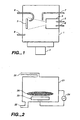
- the ion beam apparatus for producing the preferred embodiment of the present invention is illustrated schematically in FIG. 1.
- Vacuum chamber 1 is evacuated into the high vacuum region by first pumping with a rough vacuum pump (not shown) and then by a high vacuum pump 2.
- Pump 2 can be a diffusion pump, turbomolecular pump, cryogenic pump (“cryopump”), or other high vacuum pumps known in the art.
- Use of a diffusion pump with a cryogenically cooled coil for pumping water vapor is a preferred high vacuum pumping arrangement for producing the products of the present invention.
- cryopumps with carbon adsorbents is somewhat less advantageous than other high vacuum pumps because such cryopumps have a low capacity for hydrogen which is generated by the ion beam sources used to produce the products of the present invention. The low capacity for hydrogen results in the need to frequently regenerate the adsorbent in the cryopumps.
- Substrates to be coated are mounted on substrate holder 3, which may incorporate tilt, simple rotation, planetary motion, or combinations thereof.
- substrate holder 3 may incorporate tilt, simple rotation, planetary motion, or combinations thereof.
- domed planetary substrate holders may be used.
- the substrate holder can be in the vertical or horizontal orientation, or at any angle in between. Vertical orientation, substrates facing downward is preferred to minimize particulate contamination of the substrates, but if special precautions such as low turbulence vacuum pumping and careful chamber maintenance are practiced, the substrates can be mounted in the horizontal position and held in place by gravity. This horizontal mounting is advantageous from the point of view of easy fixturing of small substrates which are not easily clamped in place. This horizontal geometry can be most easily visualized by rotating the illustration in FIG. 1 by 90 degrees.
- Ion beam source 4 can be any ion source known in the prior art, including Kaufman-type direct current discharge ion sources, radio frequency or microwave frequency plasma discharge ion sources, microwave electron cyclotron resonance ion sources, each having one, two, or three grids, or gridless ion sources such as the Hall Accelerator and End Hall ion source of U.S. Pat. No. 4,862,032; the description of which is incorporated by reference herein.
- the ion beam is typically charge neutralized by introduction of electrons into the beam using a neutralizer (not shown), which may be a thermionic filament, plasma bridge, hollow cathode, or other types known in the prior art.
- Ion source 4 is provided with inlets 5 and 6 for introduction of gases directly into the ion source plasma chamber.
- Inlet 5 is used for introduction of inert gases, such as argon, krypton, and xenon, for the sputter-etching.
- oxygen may be introduced in inlet 6, and used independently or mixed with an inert gas to provide chemically-assisted sputter-etching, e.g. for plastic substrates.
- Inlet 6 is used for introduction of reactive gases such as hydrocarbons (e.g. methane, acetylene, cyclohexane), siloxanes, silazanes, oxygen, nitrogen, hydrogen, ammonia, and similar gases for the coating deposition.
- the reactive gases can be mixed with an inert gas to modify the properties of the resultant coating and improve the stability of the ion source.
- the reactive gases can also be introduced away from the ion source plasma chamber, but into the ion beam by inlet 7.
- Inlet 7 may contain multiple holes for the introduction of reactive gases, or may be a "gas distribution ring”.
- reactive gases for the deposition e.g. oxygen and ammonia, can be introduced at or near the substrate by inlet 8, or into the chamber background by inlet 9.
- the reactive gases introduced by inlet 8 modify the properties of the coating by chemical reaction at the surface of the coating during deposition.
- multiple ion sources 4 can be utilized and operated simultaneously. Operation of the ion sources can be sequenced for the case in which different coating materials are deposited from each ion source. As described in U.S. Pat. No. 4,490,229, an additional ion source (not shown) can be used to co-bombard the substrates during coating deposition to alter the film properties.
- FIG. 2 An example of an ion-assisted plasma deposition apparatus is shown schematically in FIG. 2.
- the coating is carried out in a vacuum chamber 21, which is fabricated according to the techniques known in the art.
- Vacuum chamber 21 is evacuated using the vacuum pumping port 22 which is connected to a vacuum pump (not shown).
- the pump can be a mechanical pump or a mechanical pump/roots blower pumping system.
- the substrate rests directly on a biased electrode 23, which is connected to the active output of a radio frequency power supply 24, while an additional electrode (not shown) and/or the walls of the grounded chamber 21 are part of the return circuit.
- a biased electrode 23 which is connected to the active output of a radio frequency power supply 24
- an additional electrode (not shown) and/or the walls of the grounded chamber 21 are part of the return circuit.
- the substrates Prior to coating by plasma deposition, the substrates are etched with energetic ions and/or reactive species produced in plasma 26.
- the plasma is typically produced using an inert gas (e.g. argon) or a reactive gas (e.g. hydrogen or oxygen) depending on the substrate to be coated.
- the gases used for the etching step are introduced through a gas introduction system 25.
- the deposition process is initiated.
- the precursor gases can be introduced in the chamber by a variety of methods known in the art. Volatile precursors can, for example, be heated in some type of vessel and can be introduced directly into the vacuum chamber simply through a metering valve or by means of special mass flow controllers.
- the precursor gases are introduced into the plasma 26 through the gas introduction system 25.
- Operating pressures are typically in the range of about 10 -3 Torr to about I Torr and are determined by the gas flow and the pumping speed.
- the pumping speed may be adjusted through the use of an adjustable aperture in the pumping port 22.
- a cryogenic trap (not shown) can be included in the pumping system to enhance flow rates of condensible precursors, and to protect the pumps from contamination.
- the plasma is initiated and sustained, in this embodiment, by collisions between gas molecules and free electrons oscillating in the radio frequency electric field.
- Other means of sustaining the plasma are also known such as microwave or direct current discharges.
- the radio frequency plasma produces large electric fields near the electrode which tend to repel electrons and draw positive ions toward the electrode surfaces.
- a capacitively coupled electrode 23, which is connected to the power supply 24 through a capacitor, can develop a direct current potential relative to ground. This potential difference is referred to as the bias voltage, and can be measured by an external circuit. In highly asymmetric capacitively coupled systems, where there is a large difference in the electrode surface areas, the bias voltage is an approximate measure of the energy of the ions impacting the smaller electrode.
- a conductor If a conductor is placed on an electrode 23, it will in effect become part of the electrode 23 and can be coated uniformly regardless of its shape, with some limitations. Sheets or films of plastic can be just as easily coated by placing them in intimate contact with electrode 23.
- the preferred method to produce the product of the present invention can be carried out in a batch-type vacuum deposition system, in which the main vacuum chamber is evacuated and vented to atmosphere after processing each batch of parts; a load-locked deposition system, in which the main vacuum deposition chamber is maintained under vacuum at all times, but batches of parts to be coated are shuttled in and out of the deposition zone through vacuum-to-air load locks; or in-line processing vacuum deposition chambers, in which parts are flowed constantly from atmosphere, through differential pumping zones, into the deposition chamber, back through differential pumping zones, and returned to atmospheric pressure.
- the substrate is first chemically cleaned to remove contaminants, such as residual hydrocarbons and other unwanted materials, from the substrate manufacturing and handling processes.
- Ultrasonic cleaning in solvents, or other aqueous detergents as known in the art is effective. Details of the cleaning procedure depend upon the nature of the contamination and residue remaining on the part after manufacture and subsequent handling. It has been found that it is critical for this chemical cleaning step to be effective in removing surface contaminants and residues, or the resulting adhesion of the coating will be poor.
- the substrate is inserted into a vacuum chamber, and the air in the chamber is evacuated.
- the vacuum chamber is evacuated to a pressure of 1 x 10 -5 Torr or less to ensure removal of water vapor and other contaminants from the vacuum system.
- the required level of vacuum which must be attained prior to initiating the next step must be determined by experimentation.
- the vacuum chamber is evacuated to 5 x 10 -3 Torr or less. The exact level of vacuum is dependent upon the nature of the substrate material, the sputter-etching rate, the constituents present in the vacuum chamber residual gas, and the details of the coating process. It is not desirable to evacuate to lower pressures than necessary, as this slows down the process and reduces the throughput of the coating system.
- the substrate surface is bombarded by energetic ions or exposed to reactive species to remove residual contaminants, e.g. any residual hydrocarbons, surface oxides and other unwanted materials not removed in the first step, and to activate the surface.
- This etching of the substrate surface is required to achieve high adhesion between the substrate surface and the coating layer(s).
- the etching can be carried out with inert gases such as argon, krypton, and xenon. Additionally, hydrogen or oxygen may be added to the inert gases or used independently to etch and activate the surface.
- the ion energy is greater than 20 eV. Ion energies as high as 2000 eV can be used, but ion energies less than 500 eV result in the least amount of atomic scale damage to the substrate.
- a coating layer is deposited on the substrate by a deposition flux which includes energetic ions and contains the elements C, Si, H, O, and optionally N.
- the deposition flux is generated by introducing precursor gases containing the elements C, Si, H, O, and optionally N, into a plasma. These precursor gases may be blended with other inert gases, e.g. argon.
- the precursor gases undergo "activation" in the plasma or in the ion beam itself. Examples of “activation” include, but are not limited to simple electronic excitation, ionization, chemical reaction with other species, ions and neutrals, which may be electronically excited, and decomposition into simpler ionic or neutral species which may be electronically excited.
- Ions are extracted from the plasma or ion source and strike the surface to be coated with energies from about 10 to about 1500 eV.
- the ion impact energy depends on the electric field between the point of origin of the ion and the sample, and the loss of energy due to collisions which occur between the ion and other ionic or neutral species prior to the impingement of the ion onto the substrate.
- Other activated species may also condense on the substrate surface.
- Neutral species will strike the surface with a variety of energies, from thermal to 100's of eV, depending on the origin of the neutral.
- This highly energetic deposition process produces highly adherent, very dense and hard coatings on the substrate surface. The density, hardness and other properties of the coating are all very dependent on the energetics of the deposition process as well as the precursor gases used.
- the primary control parameters are the silicon precursor gas flow, the oxygen gas flow, the pumping speed, and the beam energy and current density.
- the primary control parameters are the oxygen to silicon precursor flow rate ratio, the bias voltage, and the substrate temperature. The useful range of the latter is, however, limited for temperatures sensitive substrates such as plastics.
- Other process parameters that affect the coating properties are the total flow rate, discharge power, pressure, size and shape of electrodes, and the presence of external magnetic fields.
- Suitable silicon precursors are the following:
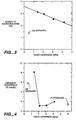
- FIG. 3 An example of the coating properties within the scope of the present invention is shown in FIG. 3, where the relationship between strain to microcracking and hardness is displayed for a series of coatings deposited by the radio frequency plasma method on polycarbonate substrates.
- the coatings were made from various O 2 /hexamethyldisiloxane mixtures, with the harder materials produced with higher O 2 /hexamethyldisiloxane flow ratios. Details of the process conditions are provided in Example A. These data indicate an inverse relationship between hardness and flexibility; soft materials tend to be flexible, while hard materials are generally not. Yet, surprisingly, General Electric's Margard MRS (a commercially available polysiloxane coating) is both soft and brittle. The strain to microcracking/hardness performance of MRS is also shown in FIG. 3. It was found that other wet chemical polysiloxane coatings performed similarly.
- FIG. 4 the Taber abrasion performance (CS10 wheels, 300 cycles, 500 g/wheel) of the radio frequency plasma-deposited coatings described in Example A below, is plotted as a function of the coating hardness. Data points for MR5 and plateglass (S-31) are also shown in FIG. 4. Totally unexpectedly, it was found that the RF plasma-deposited coatings of the present invention with hardness as low as 2 GPa experienced as little or less damage in this severe abrasion test than the much harder plateglass (with 6 GPa hardness). The coatings with hardness greater than 2 GPa clearly provide much better abrasion protection than does MRS. In addition, these coatings have very good optical properties, and are also flexible as FIG. 3 shows.
- the surprising abrasion performance may in fact be due to the high strain to microcracking of these coatings.
- Soft substrates provide little mechanical support for the coating against penetration of abrading asperities.
- the onset of the coating failure which is initiated by tensile fracture at the coating-substrate interface, occurs at lower penetration depths with brittle coatings.
- deep scratches in brittle coatings are usually more noticeable due to debris formation, jagged edges, and wider scratch grooves, all of which tend to scatter light.
- the deposition process conditions are not changed during the coating process, resulting in a single layer coating.
- the single layer coating can be from about 1 to about 100 microns thick in order to provide the required abrasion protection.
- a variety of different substrate materials can be coated including but not limited to polymethylmethacrylate, polycarbonate, acrylics, poly(allyl diglycolcarbonate) which is also known as "CR-39", and co-polymers and blends thereof; soft metals such as copper, brass and aluminum. Products which can benefit from this coating include but are not limited to sunglass lenses (both plano and ophthalmic), safety lenses, ophthalmic lenses, bar code scanner windows, and ornamental hardware such as brass switch plates.
- Polymer substrates may be coated with an adhesion-enhancing layer of less than 10 microns thickness from materials including but not limited to acrylic or polysiloxane polymers.
- DLC is an outstanding abrasion-resistant material. Therefore, for cases where an extremely hard, inert, abrasion-resistant coating is required, DLC is a preferred coating. It has been found that deposition of interlayer materials which contain silicon atoms onto the substrate prior to deposition of the DLC layer results in highly adherent DLC coatings with outstanding wear resistance properties. It is currently believed that reaction between silicon atoms in the interlayer material and the carbon atoms in the DLC layer is critical for the DLC coating to exhibit excellent adhesion. Therefore, the coating of the present invention is an excellent adhesion layer for the DLC.
- the thickness of the DLC coating can be between 50 ⁇ and approximately 100 microns. Thinner DLC coatings, on the order of 50 ⁇ are useful when the main function of the DLC layer is to provide a low-friction surface, or chemical protection. Other low friction layers, such as boron nitride, tin oxide, indium tin oxide, aluminum oxide and zirconium oxide, can be used with the present invention. Thicker DLC layers are useful when protection from severe abrasion is required.
- deposition methods may be used for the formation of the DLC coatings of the present invention, including but not limited to direct ion beam deposition, and radio frequency plasma deposition as in U.S. Patent No. 4,382,100.
- Methane or cyclohexane are preferred as the hydrocarbon source gases, but other hydrocarbon gases, such as acetylene, butane, and benzene can be used as well.
- Hydrogen and inert gases e.g. argon, krypton, and xenon, may be introduced into the ion source plasma to modify the DLC film properties.
- the ion impact energy used in the DLC deposition process may be in the range of approximately 20 eV to approximately 1000 eV. Ion energies in the range of about 20 eV to about 300 eV are most preferred to minimize heating of the substrate during deposition.
- the abrasion-resistant coating may comprise multiple layers of materials with at least two different refractive indicies.
- the coatings of the present invention may be used as either a low refractive index layer, e.g. refractive index of approximately 1.5, or the high refractive index layer.
- other high index optical materials known in the art such as titanium dioxide and zirconium oxide may be used as the high index layer. If properlly designed and deposited, as is know in the prior art, these coatings may be anti-reflective in the visible spectrum. Additionally, highly reflective coatings can also be designed and deposited in a similar fashion using techniques known in the prior art.
- the materials with different refractive indices can be produced by changing the deposition conditions, e.g. precursor gases, pressures, etc.
- the deposition process on the substrates is terminated, the vacuum chamber pressure is increased to atmospheric pressure, and the coated substrates are removed from the vacuum chamber.
- a series of coatings were deposited on 7" diameter optical grade polycarbonate discs (1/8" thick), which were set on the powered electrode of a Plasmalab 80 radio-frequency diode reactor.
- the substrates were purchased with protective cling wrap, which was removed as the last step prior to pump down. In each run the vacuum chamber was then evacuated to a pressure less than 5 x 10 -3 Torr.
- Each substrate was plasma cleaned in a O 2 plasma (100 mTorr, 50 Watts (W)) for 2 minutes. This removed nearly 3000 A of polycarbonate. The O 2 plasma was extinguished, and then mixtures of hexamethyldisiloxane (HMDSO) and O 2 were admitted to the vacuum system. The power was set at 300 W.
- HMDSO hexamethyldisiloxane
- the strain to microcracking values were then calculated from the critical radii of curvature.
- the samples were Taber abraded by CS 10 wheels for 300 cycles using 500 g weights.
- the abrasion damage was quantified by the difference in haze before and after abrasion. Haze values were obtained in accordance to ASTM D 1003, using a Gardner hazemeter. Values for the yellow index (Y 1 ) were calculated from transmission spectra in the visible range according to ASTM D1925.
- the strain to microcracking and Taber abrasion results are shown as functions of the indentation hardness in FIGS. 3 and 4, respectively, and the results of the other characterizations are presented below in Table 1.
- the three coatings made from mixtures of HMDSO and O 2 are flexible and softer than glass, yet exhibit excellent abrasion resistance. They exhibit good optical properties in that they are highly transmissive in the visible, and have yellow index and haze values less than 5 and 2%, respectively. The yellow index values were obtained several days after the samples were made. It was observed in the course of this investigation that those radio frequency-deposited organosilicon samples that are produced with visible yellowness (with yellow index greater than 2.5), particularly those grown from organosiloxane feed gases, undergo a noticeable reduction in color when they are exposed to ambient conditions.
- the samples were sputter etched for 5 minutes with an argon ion beam generated in an End Hall ion source (manufactured by Commonwealth Scientific as Mark II) using 10 sccm argon gas introduced directly into the plasma chamber of the ion source.
- the anode potential was 30 volts while the current was 5.8 amps (ion beam current approximately 1.15 amps).
- the electron source for the End Hall ion source was a hollow cathode operated on 3 sccm argon gas. After sputter-etching the substrates, approximately 16 sccm of octamethylcyclotetrasiloxane was introduced into the argon beam through nozzles located approximately 1" downstream of the ion source.
- the anode potential was 58 volts while the anode current was 5.8 amps (ion beam current approximately 1.5 amps). After operating for 3.5 minutes with these conditions, 10 sccm of oxygen gas was introduced. After operating for an additional 30 seconds, the oxygen flow was increased to 30 sccm. After an additional 30 seconds, the oxygen flow was increased to 50 sccm. After an additional 30 seconds, the oxygen flow was increased to 70 sccm and the argon was shut off. The anode potential was 56 volts and the anode current was 5.72 amps (ion beam current approximately 1.5 amps). The chamber pressure was 1.45 x 10 -3 Torr.
- the ion source plasma and ion beam were extinguished 40 minutes after the first introduction of the octamethylcyclotetrasiloxane.
- the chamber was brought to atmospheric pressure and the samples were removed.
- the coated samples were water-clear when viewed in visible light. Approximately 5.5 microns of coating was deposited onto the samples.
- the stress of the coating was 7.7 x 10 8 dynes/cm 2 .
- the haze measured on the CR-39 samples was less than 0.4%.
- the 2" x 2" x 0.125" piece of coated CR-39 was tested with a Taber abrader using 500 grams load with CS-10F wheels (total of 1 kg load). After 500 cycles, the change in haze was determined to be 0.65%. Glass tested in an identical fashion had a change in haze of 0.69% haze after 500 cycles.
- the coating contained carbon, silicon, oxygen, and hydrogen.
- Two CR-39 lenses, and two CR-39 2" x 2" x 0.125" pieces were ultrasonically cleaned in isopropanol and then dried using nitrogen gas.
- the samples were mounted on a 18-inch diameter aluminum disk with Kapton tape.
- the disk was mounted in a stainless steel vacuum chamber which was pumped with a 10" diffusion pump. The chamber was evacuated to a pressure of 1.6 x 10 -5 Torr.
- the samples were sputter-etched for 5 minutes using an argon ion beam generated in the End Hall ion source used in Example B with 17.4 sccm of argon gas directly into the plasma chamber of the ion source, an anode potential of 80 volts, and an anode current of 4.22 amps (ion beam current approximately 0.85 amp).
- the electron source for the End Hall ion source was a hollow cathode.
- a shutter was then placed between the ion source and the substrates to block the ion beam, and 100 sccm of oxygen gas was run into the plasma chamber of the ion source, the argon was turned off, and octamethylcyclotetrasiloxane was allowed into the chamber through nozzles located approximately I" downstream of the ion source.
- the anode potential was 72 volts and the anode current was 5.57 amps (ion beam current approximately 1.2 amps).
- the pressure during this process was 1.25 x 10 -3 Torr. After 72 minutes of operation at this condition, the ion source plasma and ion beam were extinguished and the chamber was brought to atmospheric pressure, and the substrates were removed.
- the samples were water-clear in visible light.
- the coating thickness was 7.6 microns and the compressive stress was 5.7 x 10 8 dynes/cm 2 .
- the hardness of the coating (measured by nanoindentation) was 3.4 GPa.
- the hardness of quartz measured by the same technique was 10 GPa.
- a thin (0.005 inch) PET film was tensioned over a nearly flat but slightly curved saddle-shaped electrode in the Plasmalab 80 reactor.
- O 2 plasma pretreatment 0.1 Torr, 50W
- a 1:1 mixture of hexamethyldisiloxane:O 2 100 sccm of each was admitted into the chamber and deposition was carried out for 4 minutes at 0.15 Torr pressure with 250 W power and the electrode temperature at 20°C.
- a colorless, clear coating approximately 4 ⁇ m thick was produced.
- the PET side of this sample was then laminated onto soft 0.03 inch PVC film.
- the coated side of the laminate was very scratch resistant to #0 grade steel wool. Similar coatings on PET film substrates exhibited glass-like abrasion resistance to Taber abrasion.
- the samples were sputter etched for 2 minutes with an argon ion beam generated in the End Hall ion source (used in the above examples) using 3 sccm argon gas introduced directly into the plasma chamber of the ion source.
- the anode potential was 50 volts while the current was 5.6 amps.
- the electron source for the End Hall ion source was a hollow cathode operated on 3 sccm argon gas.
- approximately 16 sccm of octamethylcyclotetrasiloxane was introduced into the argon beam through nozzles located approximately 1" downstream of the ion source.
- the anode potential was 59 volts while the anode current was 5.8 amps (ion beam current approximately 1.5 amps).
- 70 sccm of oxygen gas was introduced into the plasma chamber of the ion source and the argon flow was reduced to 0.0 sccm.
- the anode potential was 57 volts and the anode current was 5.79 amps (ion beam current approximately 1.5 amps).
- the chamber pressure was 1.4 x 10 -3 Torr.
- the ion source plasma and ion beam were extinguished 40 minutes after the first introduction of the octamethylcyclotetrasiloxane.
- the chamber was brought to atmospheric pressure and the samples were removed.
- the coated samples were water-clear when viewed in visible light. Approximately 4.8 microns of coating was deposited onto the samples.
- the stress of the coating was 6.4 x 10 8 dynes/cm 2 .
- the tensile strain to microcracking of the coating was determined using a four point bend technique. Coated polycarbonate pieces, 1 cm x 10 cm, were cut from the 8" diameter disk and mounted in the four point bend apparatus. The samples were bent until microcracking of the coating was observed. The radius of curvature was measured and the strain was calculated. The results indicate that the strain to microcracking was 2.1 - 2.2%.
- All of the examples demonstrate highly optically transparent, water-clear, low-stress, adherent, hard, abrasion-resistant coatings containing silicon, carbon, oxygen, and hydrogen, which coatings can be deposited onto plastic substrates at high deposition rates. These coatings exhibited hardness between that of wet chemical-produced polysiloxane coatings and that of glass. When applied to plastic substrates, these coatings, which contain silicon, carbon, oxygen, and hydrogen, produced Taber abrasion resistance test results equivalent to that of glass. These coatings are particularly useful in applications where optical plastic substrates require improved abrasion protection (e.g. plastic sunglass or ophthalmic lenses). Similar coatings which contain nitrogen can be made.
- a unique advantage of the use of the ion beam method for producing these materials is the relationship between stress and hardness. It is well known in the prior art that stress and hardness are often strongly related. Typically, the greater the compressive stress, the harder the material. For the case of the Si, C, O, H materials produced by injecting siloxane precursors into an oxygen ion beam, it was unexpectedly found that by increasing the ratio of oxygen to siloxane precursor, the coating hardness was increased, while the compressive stress was simultaneously decreased. By this method, it is possible to produce hard, abrasion-resistant coatings which are under tensile stress, or are nearly stress-free. This is a very unexpected result for an energetic deposition process. and a key technical advantage of the ion beam process.
- the coatings of the present invention Using radio frequency plasma or ion beam processes to deposit the coatings of the present invention, very high deposition rates can be achieved while maintaining low substrate temperature.
- the coatings are very adherent and provide outstanding abrasion protection.
- coated plastic substrates such as lenses, which have abrasion resistance equal to that of glass can be produced. Because of the high coating deposition rates which can be attained, the invention provides an economical manufacturing process.
- the present invention provides an improved method for producing highly protective and abrasion-resistant coatings on a variety of substrates, including optical plastics.
- Highly important technical advantages of the present invention include outstanding adhesion of the coatings, outstanding abrasion resistance, high transparency, high strain to microcracking, and ease and flexibility of mass production.
Landscapes
- Chemical & Material Sciences (AREA)
- Physics & Mathematics (AREA)
- Engineering & Computer Science (AREA)
- Plasma & Fusion (AREA)
- General Chemical & Material Sciences (AREA)
- Chemical Kinetics & Catalysis (AREA)
- Organic Chemistry (AREA)
- Materials Engineering (AREA)
- Mechanical Engineering (AREA)
- Metallurgy (AREA)
- General Physics & Mathematics (AREA)
- Optics & Photonics (AREA)
- Health & Medical Sciences (AREA)
- Medicinal Chemistry (AREA)
- Polymers & Plastics (AREA)
- Inorganic Chemistry (AREA)
- Chemical Vapour Deposition (AREA)
- Physical Vapour Deposition (AREA)
- Paints Or Removers (AREA)
- Polymers With Sulfur, Phosphorus Or Metals In The Main Chain (AREA)
- Application Of Or Painting With Fluid Materials (AREA)
Claims (28)
- Abrasionsverschleißfestes beschichtetes Substratprodukt, das durch das Verfahren eines der Ansprüche 15 - 28 erhalten werden kann, umfassend ein Substrat und ein abrasionsverschleißfestes Beschichtungsmaterial, das Kohlenstoff, Wasserstoff, Silizium und Sauerstoff enthält; wobei das abrasionsverschleißfeste Beschichtungsmaterial die Eigenschaften einer Nanoeindringhärte im Bereich von ca. 2 bis 5 GPa und einer Dehnung bis Mikroriss von über ca. 1% hat.
- Produkt nach Anspruch 1, bei dem das abrasionsverschleißfeste Beschichtungsmaterial im sichtbaren Spektrum eine Transparenz von über 85% hat.
- Produkt nach Anspruch 1, bei dem das abrasionsverschleißfeste Beschichtungsmaterial eine Veränderung bei der Trübung von weniger als 2%, gemessen durch ASTM D1003 während des Abriebs nach Taber, unterliegt, wie in ASTM D1044 beschrieben ist.
- Produkt nach Anspruch 1, bei dem die Dicke des abrasionsverschleißfesten Beschichtungsmaterials im Bereich von ca. 1 µm bis ca. 100 µm liegt.
- Produkt nach einem der Ansprüche 1 bis 4, bei dem das abrasionsverschleißfeste Beschichtungsmaterial auch Stickstoff enthält.
- Produkt nach Anspruch 1, bei dem das Substrat entweder ein Metall oder ein Polymer umfasst.
- Produkt nach Anspruch 6, bei dem das Substrat ein Polymer ist.
- Produkt nach Anspruch 7, bei dem das Polymersubstrat aus Polymethylmethacrylat, Polycarbonat, Acrylharzderivaten, Poly(allyldiglycolcarbonat), Copolymeren und Mischungen davon ausgewählt ist.
- Produkt nach Anspruch 7 oder 8, bei dem das beschichtete Substratprodukt darüber hinaus eine adhäsionsverstärkende Polymerschicht zwischen dem Substrat und dem abrasionsverschleißfesten Beschichtungsmaterial umfasst.
- Produkt nach Anspruch 9, bei dem die adhäsionsverstärkende Schicht entweder ein Acrylpolymer oder ein Polysiloxanpolymer ist.
- Produkt nach Anspruch 9 oder 10, bei dem die adhäsionsverstärkende Schicht weniger als 10 µm dick ist.
- Produkt nach einem der Ansprüche 1 bis 5, bei dem das Substrat ein augenheilkundliches Sehkorrekturglas, ein Sonnenbrillenglas, eine Flachlinse, eine Sicherheitslinse oder das Fenster eines Strichcodescanners umfasst.
- Produkt nach einem der Ansprüche 1 bis 12, bei dem das abrasionsverschleißfeste Beschichtungsmaterial mehrere Schichten mit mindestens zwei unterschiedlichen Brechungsexponenten umfasst, um Reflexion bei vorbestimmten Wellenlängen zu reduzieren.
- Produkt nach einem der Ansprüche 1 bis 13, bei dem das abrasionsverschleißfeste Beschichtungsmaterial darüber hinaus eine äußere Schicht aus diamantartigem Kohlenstoff umfasst.
- Verfahren zum Abscheiden eines aus C, H, Si und O bestehenden, abrasionsverschleißfesten Beschichtungsmaterials auf einem Grundsubstrat, welches Verfahren umfasst:(a) die Oberfläche des Substrats chemisch zu reinigen, um Verunreinigungen zu entfernen;(b) das Substrat in einer Unterdruckbeschichtungskammer anzubringen und die Luft aus der Kammer abzuziehen;(c) die Oberfläche des Substrats mit einem Material zu ätzen, das aus der Gruppe ausgewählt ist, die aus energiereichen Ionen, reaktiven Arten und Gemischen davon besteht, um Restverunreinigungen noch weiter zu entfernen und um die Oberfläche zu aktivieren;(d) auf der Oberfläche des Substrats eine Schicht des abrasionsverschleißfesten Materials abzuscheiden, indem das Substrat einem kohlenstoff-, wasserstoff-, siliziumund sauerstoffhaltigen Abscheidungsfluss ausgesetzt wird, bei dem die chemischen Vorläufer für den Abscheidungsfluss Siloxane, Silazane und Gemische davon mit Sauerstoff umfassen und durch ein Plasma erzeugt wurden, wobei der Abscheidungsfluss durch das Plasma aktiviert und das Substrat während der Abscheidung durch die energiereichen Ionen beschossen wird;(e) den Druck in der Unterdruckkammer auf Normaldruck anzuheben; und(f) ein Produkt zu entnehmen, das mit dem abrasionsverschleißfesten Material mit den Eigenschaften einer Nanoeindringhärte im Bereich von ca. 2 bis 5 GPa und einer Dehnung bis Mikroriss von über ca. 1% beschichtet ist.
- Verfahren nach Anspruch 15, bei dem der Abscheidungsfluss auch Stickstoff und das abrasionsverschleißfeste Beschichtungsmaterial auch Stickstoff enthält.
- Verfahren nach Anspruch 15 oder 16, bei dem der Abscheidungsfluss durch ein Hochfrequenzplasma aktiviert wird.
- Verfahren nach Anspruch 15 oder 16, bei dem der Abscheidungsfluss durch ein Mikrowellenplasma aktiviert wird.
- Verfahren nach Anspruch 15 oder 16, bei dem der Abscheidungsfluss durch ein Gleichstromplasma aktiviert wird.
- Verfahren nach einem der Ansprüche 15 bis 19, bei dem die chemischen Vorläufer für den Abscheidungsfluss Stoffe enthalten, die aus der Gruppe ausgewählt sind, die aus Hexamethyldisiloxan, Tetramethylcyclotetrasiloxan, Octamethylcyclotetrasiloxan und Gemischen davon besteht.
- Verfahren zum Abscheiden eines aus C, H, Si und O bestehenden, abrasionsverschleißfesten Beschichtungsmaterials auf einem Grundsubstrat, welches Verfahren umfasst:(a) die Oberfläche des Substrats chemisch zu reinigen, um Verunreinigungen zu entfernen;(b) das Substrat in einer Unterdruckbeschichtungskammer anzubringen und die Luft aus der Kammer abzuziehen;(c) die Oberfläche des Substrats mit einem Material zu ätzen, das aus der Gruppe ausgewählt ist, die aus energiereichen Ionen, reaktiven Arten und Gemischen davon besteht, um Restverunreinigungen noch weiter zu entfernen und um die Oberfläche zu aktivieren;(d) auf der Oberfläche des Substrats eine Zwischenschicht des abrasionsverschleißfesten Materials abzuscheiden, indem das Substrat einem kohlenstoff-, wasserstoff-, siliziumund sauerstoffhaltigen Abscheidungsfluss ausgesetzt wird, wobei das abrasionsverschleißfeste Material die Eigenschaften einer Nanoeindringhärte im Bereich von ca. 2 bis 5 GPa und einer Dehnung bis Mikroriss von über ca. 1% hat, und bei dem die chemischen Vorläufer für den Abscheidungsfluss Siloxane, Silazane und Gemische davon mit Sauerstoff umfassen und durch ein Plasma erzeugt wurden, wobei der Abscheidungsfluss durch das Plasma aktiviert und das Substrat während der Abscheidung durch die energiereichen Ionen beschossen wird;(e) auf der Zwischenschicht eine äußere Schicht aus diamantartigem Kohlenstoff abzuscheiden;(f) den Druck der Unterdruckkammer auf Normaldruck anzuheben; und(g) ein beschichtetes abrasionsverschleißfestes Produkt zu entnehmen.
- Verfahren nach Anspruch 21, bei dem der Abscheidungsfluss durch ein Hochfrequenzplasma aktiviert wird.
- Verfahren nach Anspruch 21, bei dem der Abscheidungsfluss durch ein Mikrowellenplasma aktiviert wird.
- Verfahren nach Anspruch 21, bei dem der Abscheidungsfluss durch ein Gleichstromplasma aktiviert wird.
- Verfahren nach einem der Ansprüche 21 bis 24, bei dem die chemischen Vorläufer für den Abscheidungsfluss Stoffe enthalten, die aus der Gruppe ausgewählt sind, die aus Hexamethyldisiloxan, Tetramethylcyclotetrasiloxan, Octamethylcyclotetrasiloxan und Gemischen davon besteht.
- Verfahren nach einem der Ansprüche 22 bis 25, bei dem die nicht kristalline diamantartige Kohlenstoffschicht eine Dicke von 50 Å bis 100 µm hat.
- Verfahren nach einem der Ansprüche 22 bis 26, bei dem der Abscheidungsfluss auch Stickstoff enthält, und das abrasionsverschleißfeste Beschichtungsmaterial auch Stickstoff enthält.
- Verfahren nach einem der Ansprüche 22 bis 27, bei dem das abrasionsverschleißfeste Material im sichtbaren Spektrum eine Transparenz von über 85% hat.
Applications Claiming Priority (3)
| Application Number | Priority Date | Filing Date | Title |
|---|---|---|---|
| US08/205,954 US5618619A (en) | 1994-03-03 | 1994-03-03 | Highly abrasion-resistant, flexible coatings for soft substrates |
| US205954 | 1994-03-03 | ||
| PCT/US1995/002761 WO1995024275A2 (en) | 1994-03-03 | 1995-03-01 | Highly abrasion-resistant, flexible coatings for soft substrates |
Publications (3)
| Publication Number | Publication Date |
|---|---|
| EP0748259A1 EP0748259A1 (de) | 1996-12-18 |
| EP0748259A4 EP0748259A4 (de) | 1998-07-15 |
| EP0748259B1 true EP0748259B1 (de) | 2004-09-22 |
Family
ID=22764360
Family Applications (1)
| Application Number | Title | Priority Date | Filing Date |
|---|---|---|---|
| EP95913563A Expired - Lifetime EP0748259B1 (de) | 1994-03-03 | 1995-03-01 | Hochabriebfeste, flexible beschichtungen für weiche substrate |
Country Status (6)
| Country | Link |
|---|---|
| US (2) | US5618619A (de) |
| EP (1) | EP0748259B1 (de) |
| JP (1) | JPH10500609A (de) |
| AT (1) | ATE276835T1 (de) |
| DE (1) | DE69533546T2 (de) |
| WO (1) | WO1995024275A2 (de) |
Cited By (5)
| Publication number | Priority date | Publication date | Assignee | Title |
|---|---|---|---|---|
| DE102007000611A1 (de) | 2007-10-31 | 2009-05-07 | Fraunhofer-Gesellschaft zur Förderung der angewandten Forschung e.V. | Kratzfeste und dehnbare Korrosionsschutzschicht für Leichtmetallsubstrate |
| DE102009002780A1 (de) | 2009-04-30 | 2010-11-11 | Fraunhofer-Gesellschaft zur Förderung der angewandten Forschung e.V. | Metallsubstrate mit kratzfester und dehnbarer Korrosionsschutzschicht und Verfahren zu deren Herstellung |
| US7857905B2 (en) | 2007-03-05 | 2010-12-28 | Momentive Performance Materials Inc. | Flexible thermal cure silicone hardcoats |
| US8691915B2 (en) | 2012-04-23 | 2014-04-08 | Sabic Innovative Plastics Ip B.V. | Copolymers and polymer blends having improved refractive indices |
| DE102023125172A1 (de) | 2023-09-18 | 2025-03-20 | Fraunhofer-Gesellschaft zur Förderung der angewandten Forschung eingetragener Verein | Plasmapolymerer Festkörper, entsprechende Verwendungen und entsprechende Verfahren |
Families Citing this family (135)
| Publication number | Priority date | Publication date | Assignee | Title |
|---|---|---|---|---|
| US5508368A (en) * | 1994-03-03 | 1996-04-16 | Diamonex, Incorporated | Ion beam process for deposition of highly abrasion-resistant coatings |
| US5846649A (en) * | 1994-03-03 | 1998-12-08 | Monsanto Company | Highly durable and abrasion-resistant dielectric coatings for lenses |
| US6468642B1 (en) * | 1995-10-03 | 2002-10-22 | N.V. Bekaert S.A. | Fluorine-doped diamond-like coatings |
| US5918150A (en) * | 1996-10-11 | 1999-06-29 | Sharp Microelectronics Technology, Inc. | Method for a chemical vapor deposition of copper on an ion prepared conductive surface |
| US5879775A (en) * | 1996-12-12 | 1999-03-09 | Eastman Kodak Compnay | Protective inorganic and DLC coatings for plastic media such as plastic cards |
| EP0885983A1 (de) * | 1997-06-19 | 1998-12-23 | N.V. Bekaert S.A. | Verfahren zur Beschichtung eines Substrates mit einer diamantartigen Nanocomposit-Zusammensetzung |
| US6110544A (en) * | 1997-06-26 | 2000-08-29 | General Electric Company | Protective coating by high rate arc plasma deposition |
| US6893720B1 (en) * | 1997-06-27 | 2005-05-17 | Nissin Electric Co., Ltd. | Object coated with carbon film and method of manufacturing the same |
| US6086962A (en) | 1997-07-25 | 2000-07-11 | Diamonex, Incorporated | Method for deposition of diamond-like carbon and silicon-doped diamond-like carbon coatings from a hall-current ion source |
| US6077567A (en) * | 1997-08-15 | 2000-06-20 | University Of Cincinnati | Method of making silica coated steel substrates |
| DE19748240C2 (de) * | 1997-10-31 | 2001-05-23 | Fraunhofer Ges Forschung | Verfahren zur korrosionsfesten Beschichtung von Metallsubstraten mittels Plasmapolymerisation und dessen Anwendung |
| US6660656B2 (en) | 1998-02-11 | 2003-12-09 | Applied Materials Inc. | Plasma processes for depositing low dielectric constant films |
| US6303523B2 (en) | 1998-02-11 | 2001-10-16 | Applied Materials, Inc. | Plasma processes for depositing low dielectric constant films |
| US6627532B1 (en) * | 1998-02-11 | 2003-09-30 | Applied Materials, Inc. | Method of decreasing the K value in SiOC layer deposited by chemical vapor deposition |
| US6054379A (en) * | 1998-02-11 | 2000-04-25 | Applied Materials, Inc. | Method of depositing a low k dielectric with organo silane |
| US6287990B1 (en) | 1998-02-11 | 2001-09-11 | Applied Materials, Inc. | CVD plasma assisted low dielectric constant films |
| US6593247B1 (en) * | 1998-02-11 | 2003-07-15 | Applied Materials, Inc. | Method of depositing low k films using an oxidizing plasma |
| DE19808180A1 (de) * | 1998-02-26 | 1999-09-09 | Bosch Gmbh Robert | Kombinierte Verschleißschutzschicht, Verfahren zur Erzeugung derselben, die damit beschichteten Objekte und deren Verwendung |
| US6548173B2 (en) * | 1998-04-20 | 2003-04-15 | Argonne National Laboratory | Method of produce ultra-low friction carbon films |
| US6068884A (en) * | 1998-04-28 | 2000-05-30 | Silcon Valley Group Thermal Systems, Llc | Method of making low κ dielectric inorganic/organic hybrid films |
| US6368678B1 (en) | 1998-05-13 | 2002-04-09 | Terry Bluck | Plasma processing system and method |
| US6159871A (en) | 1998-05-29 | 2000-12-12 | Dow Corning Corporation | Method for producing hydrogenated silicon oxycarbide films having low dielectric constant |
| US6667553B2 (en) | 1998-05-29 | 2003-12-23 | Dow Corning Corporation | H:SiOC coated substrates |
| US6147009A (en) | 1998-06-29 | 2000-11-14 | International Business Machines Corporation | Hydrogenated oxidized silicon carbon material |
| JP2002521247A (ja) * | 1998-07-27 | 2002-07-16 | ナムローゼ・フェンノートシャップ・ベーカート・ソシエテ・アノニム | フラットパネルディスプレイ基板用ハードコート |
| US6974766B1 (en) * | 1998-10-01 | 2005-12-13 | Applied Materials, Inc. | In situ deposition of a low κ dielectric layer, barrier layer, etch stop, and anti-reflective coating for damascene application |
| US6251802B1 (en) | 1998-10-19 | 2001-06-26 | Micron Technology, Inc. | Methods of forming carbon-containing layers |
| US6277480B1 (en) * | 1999-05-03 | 2001-08-21 | Guardian Industries Corporation | Coated article including a DLC inclusive layer(s) and a layer(s) deposited using siloxane gas, and corresponding method |
| US6475573B1 (en) * | 1999-05-03 | 2002-11-05 | Guardian Industries Corp. | Method of depositing DLC inclusive coating on substrate |
| WO2000075394A1 (en) * | 1999-06-08 | 2000-12-14 | N.V. Bekaert S.A. | A doped diamond-like carbon coating |
| US6399489B1 (en) | 1999-11-01 | 2002-06-04 | Applied Materials, Inc. | Barrier layer deposition using HDP-CVD |
| US20040028906A1 (en) * | 2000-01-04 | 2004-02-12 | Anderson Jerrel Charles | Diamond-like carbon coating on glass and plastic for added hardness and abrasion resistance |
| DE10003836C2 (de) * | 2000-01-28 | 2002-04-25 | Fraunhofer Ges Forschung | Indentor und Verwendung desselben |
| US6696157B1 (en) | 2000-03-05 | 2004-02-24 | 3M Innovative Properties Company | Diamond-like glass thin films |
| US6795636B1 (en) | 2000-03-05 | 2004-09-21 | 3M Innovative Properties Company | Radiation-transmissive films on glass articles |
| US6749813B1 (en) | 2000-03-05 | 2004-06-15 | 3M Innovative Properties Company | Fluid handling devices with diamond-like films |
| DE60116407T2 (de) * | 2000-05-09 | 2006-07-06 | Kabushiki Kaisha Riken | Amorphe oxidhaltige Kohlenstoffschicht |
| EP1158088A3 (de) * | 2000-05-26 | 2003-01-22 | Voith Paper Patent GmbH | Verfahren und Vorrichtung zur Behandlung einer Faserstoffsuspension |
| US6524755B2 (en) | 2000-09-07 | 2003-02-25 | Gray Scale Technologies, Inc. | Phase-shift masks and methods of fabrication |
| US6531398B1 (en) | 2000-10-30 | 2003-03-11 | Applied Materials, Inc. | Method of depositing organosillicate layers |
| US6537733B2 (en) * | 2001-02-23 | 2003-03-25 | Applied Materials, Inc. | Method of depositing low dielectric constant silicon carbide layers |
| US7316764B2 (en) * | 2001-03-16 | 2008-01-08 | 4 Wave, Inc. | System and method for performing sputter etching using independent ion and electron sources and a substrate biased with an a-symmetric bi-polar DC pulse signal |
| US7288293B2 (en) * | 2001-03-27 | 2007-10-30 | Apit Corp. S.A. | Process for plasma surface treatment and device for realizing the process |
| US6709721B2 (en) | 2001-03-28 | 2004-03-23 | Applied Materials Inc. | Purge heater design and process development for the improvement of low k film properties |
| US6472333B2 (en) | 2001-03-28 | 2002-10-29 | Applied Materials, Inc. | Silicon carbide cap layers for low dielectric constant silicon oxide layers |
| US6486082B1 (en) * | 2001-06-18 | 2002-11-26 | Applied Materials, Inc. | CVD plasma assisted lower dielectric constant sicoh film |
| US6926926B2 (en) * | 2001-09-10 | 2005-08-09 | Applied Materials, Inc. | Silicon carbide deposited by high density plasma chemical-vapor deposition with bias |
| US6656837B2 (en) * | 2001-10-11 | 2003-12-02 | Applied Materials, Inc. | Method of eliminating photoresist poisoning in damascene applications |
| CA2408113C (en) | 2001-10-25 | 2005-10-04 | Hoya Corporation | Optical element having antireflection film |
| US6699784B2 (en) | 2001-12-14 | 2004-03-02 | Applied Materials Inc. | Method for depositing a low k dielectric film (K>3.5) for hard mask application |
| US6890850B2 (en) * | 2001-12-14 | 2005-05-10 | Applied Materials, Inc. | Method of depositing dielectric materials in damascene applications |
| US6838393B2 (en) * | 2001-12-14 | 2005-01-04 | Applied Materials, Inc. | Method for producing semiconductor including forming a layer containing at least silicon carbide and forming a second layer containing at least silicon oxygen carbide |
| US6936309B2 (en) * | 2002-04-02 | 2005-08-30 | Applied Materials, Inc. | Hardness improvement of silicon carboxy films |
| US20030211244A1 (en) * | 2002-04-11 | 2003-11-13 | Applied Materials, Inc. | Reacting an organosilicon compound with an oxidizing gas to form an ultra low k dielectric |
| US20030194495A1 (en) * | 2002-04-11 | 2003-10-16 | Applied Materials, Inc. | Crosslink cyclo-siloxane compound with linear bridging group to form ultra low k dielectric |
| US20030194496A1 (en) * | 2002-04-11 | 2003-10-16 | Applied Materials, Inc. | Methods for depositing dielectric material |
| US6815373B2 (en) * | 2002-04-16 | 2004-11-09 | Applied Materials Inc. | Use of cyclic siloxanes for hardness improvement of low k dielectric films |
| US20030206337A1 (en) * | 2002-05-06 | 2003-11-06 | Eastman Kodak Company | Exposure apparatus for irradiating a sensitized substrate |
| WO2003101733A1 (en) * | 2002-06-04 | 2003-12-11 | Western Life Sciences, Llc | Method of forming a polymer tie layer on metal surface |
| US7105460B2 (en) * | 2002-07-11 | 2006-09-12 | Applied Materials | Nitrogen-free dielectric anti-reflective coating and hardmask |
| US6927178B2 (en) * | 2002-07-11 | 2005-08-09 | Applied Materials, Inc. | Nitrogen-free dielectric anti-reflective coating and hardmask |
| US6905773B2 (en) * | 2002-10-22 | 2005-06-14 | Schlage Lock Company | Corrosion-resistant coatings and methods of manufacturing the same |
| US6897163B2 (en) * | 2003-01-31 | 2005-05-24 | Applied Materials, Inc. | Method for depositing a low dielectric constant film |
| US6878404B2 (en) * | 2003-02-06 | 2005-04-12 | Guardian Industries Corp. | Method of depositing DLC on substrate |
| US7501148B2 (en) | 2003-11-04 | 2009-03-10 | Guardian Industries Corp. | Method of making heat treatable coated article with diamond-like carbon (DLC) and/or zirconium in coating |
| US7150849B2 (en) * | 2003-11-04 | 2006-12-19 | Guardian Industries Corp. | Heat treatable coated article with diamond-like carbon (DLC) and/or zirconium in coating |
| US7507442B2 (en) * | 2003-11-04 | 2009-03-24 | Guardian Industries Corp. | Heat treatable coated article with diamond-like carbon (DLC) and/or zirconium in coating |
| US7537801B2 (en) * | 2003-11-04 | 2009-05-26 | Guardian Industries Corp. | Heat treatable coated article with diamond-like carbon (DLC) and/or zirconium in coating |
| US7445273B2 (en) * | 2003-12-15 | 2008-11-04 | Guardian Industries Corp. | Scratch resistant coated glass article resistant fluoride-based etchant(s) |
| US20110104381A1 (en) * | 2004-01-15 | 2011-05-05 | Stefan Laure | Plasma Treatment of Large-Scale Components |
| WO2005093300A1 (en) | 2004-03-05 | 2005-10-06 | Waters Investments Limited | Valve with low friction coating |
| JP5039907B2 (ja) * | 2004-03-09 | 2012-10-03 | エグザテック・リミテッド・ライアビリティー・カンパニー | 非平面状基体のためのプラズマ被覆装置 |
| PL1740950T5 (pl) * | 2004-04-30 | 2013-03-29 | Vlaamse Instelling Voor Tech Onderzoek Vito | Immobilizacja biocząsteczek z zastosowaniem technologii z plazmą atmosferyczną |
| US7288205B2 (en) * | 2004-07-09 | 2007-10-30 | Applied Materials, Inc. | Hermetic low dielectric constant layer for barrier applications |
| US20060107599A1 (en) * | 2004-11-24 | 2006-05-25 | Guardian Industries Corp. | Flush-mounted slider window for pick-up truck with hydrophilic coating on interior surface thereof, and method of making same |
| US20060110605A1 (en) * | 2004-11-24 | 2006-05-25 | Guardian Industries Corp. | Hydrophilic coating and method of making same |
| US20080096014A1 (en) * | 2004-12-13 | 2008-04-24 | University Of South Australia | Craze Resistant Plastic Article and Method of Production |
| US8030219B1 (en) * | 2005-02-07 | 2011-10-04 | Morgan Advanced Ceramics, Inc. | Dielectric coatings and use in capacitors |
| JP2006258283A (ja) * | 2005-02-18 | 2006-09-28 | Denso Corp | 流体制御弁、および電磁弁 |
| CN101156504B (zh) * | 2005-04-11 | 2012-07-18 | 洛尔等离子技术有限公司 | 等离子喷涂设备及方法 |
| US20070020451A1 (en) * | 2005-07-20 | 2007-01-25 | 3M Innovative Properties Company | Moisture barrier coatings |
| US20070196633A1 (en) * | 2005-11-30 | 2007-08-23 | Coak Craig E | Durable transparent coatings for polymeric substrates |
| US8313812B2 (en) * | 2005-11-30 | 2012-11-20 | The Boeing Company | Durable transparent coatings for aircraft passenger windows |
| DE102006018491A1 (de) * | 2006-04-19 | 2007-10-25 | Fraunhofer-Gesellschaft zur Förderung der angewandten Forschung e.V. | Flexible plasmapolymere Produkte, entsprechende Artikel, Herstellverfahren und Verwendung |
| US20080006819A1 (en) * | 2006-06-19 | 2008-01-10 | 3M Innovative Properties Company | Moisture barrier coatings for organic light emitting diode devices |
| US7811628B2 (en) * | 2006-12-22 | 2010-10-12 | Roger Wen-Yi Hsu | Layered lenses and method of layering lenses |
| WO2008104160A2 (de) * | 2007-02-26 | 2008-09-04 | Dr. Laure Plasmatechnologie Gmbh | Vorrichtung und ein verfahren zur plasmagestützten beschichtung und oberflächenbehandlung grossvolumiger bauteile |
| US7878054B2 (en) * | 2007-02-28 | 2011-02-01 | The Boeing Company | Barrier coatings for polymeric substrates |
| US9102083B2 (en) * | 2007-09-06 | 2015-08-11 | 3M Innovative Properties Company | Methods of forming molds and methods of forming articles using said molds |
| WO2009104407A1 (ja) * | 2008-02-20 | 2009-08-27 | ダイキョーニシカワ株式会社 | 樹脂成形体 |
| US20090311539A1 (en) * | 2008-06-11 | 2009-12-17 | The Boeing Company | Wear-resistant coating for polymeric transparencies |
| JP5256441B2 (ja) * | 2008-08-22 | 2013-08-07 | 株式会社ユーテック | 透明樹脂積層体及びその製造方法 |
| DE102009000699A1 (de) | 2009-02-06 | 2010-08-12 | Fraunhofer-Gesellschaft zur Förderung der angewandten Forschung e.V. | Kunststoffsubstrat, umfassend eine flexible, transparente Schutzschicht sowie Verfahren zur Herstellung eines solchen Kunststoffsubstrates |
| TWI403413B (zh) * | 2009-04-27 | 2013-08-01 | Univ Tatung | 親疏水性可轉換複合膜及其製備方法 |
| US8365619B2 (en) * | 2009-05-05 | 2013-02-05 | The United States Of America As Represented By The Secretary Of The Army | Assembly and method for evaluating effectiveness of anti-fog coatings of eyewear lenses |
| MX350703B (es) | 2009-05-13 | 2017-09-14 | Sio2 Medical Products Inc | Metodo de gasificacion para inspeccionar una superficie revestida. |
| US7985188B2 (en) * | 2009-05-13 | 2011-07-26 | Cv Holdings Llc | Vessel, coating, inspection and processing apparatus |
| WO2013170052A1 (en) | 2012-05-09 | 2013-11-14 | Sio2 Medical Products, Inc. | Saccharide protective coating for pharmaceutical package |
| US9458536B2 (en) | 2009-07-02 | 2016-10-04 | Sio2 Medical Products, Inc. | PECVD coating methods for capped syringes, cartridges and other articles |
| BE1019159A5 (nl) * | 2010-01-22 | 2012-04-03 | Europlasma Nv | Werkwijze voor de afzetting van een gelijkmatige nanocoating door middel van een lage druk plasma proces. |
| JP2011186149A (ja) * | 2010-03-08 | 2011-09-22 | Olympus Corp | 光学部品及びその製造方法 |
| US11624115B2 (en) | 2010-05-12 | 2023-04-11 | Sio2 Medical Products, Inc. | Syringe with PECVD lubrication |
| EP2605862B1 (de) * | 2010-06-29 | 2020-04-29 | SiO2 Medical Products, Inc. | Spritze mit integrierter nadel |
| EP2402475A1 (de) | 2010-06-30 | 2012-01-04 | Fei Company | Strahleninduzierte Ablagerung bei kryogenischen Temperaturen |
| US9878101B2 (en) | 2010-11-12 | 2018-01-30 | Sio2 Medical Products, Inc. | Cyclic olefin polymer vessels and vessel coating methods |
| EP2498074A1 (de) * | 2011-03-07 | 2012-09-12 | Bronlund, Ole Einar | Weitere Verbesserung an einem Temperaturkalibrator |
| US9272095B2 (en) | 2011-04-01 | 2016-03-01 | Sio2 Medical Products, Inc. | Vessels, contact surfaces, and coating and inspection apparatus and methods |
| US20130011644A1 (en) * | 2011-07-06 | 2013-01-10 | Innovation & Infinity Global Corp. | Conductive multilayer structure and touch panel having the same |
| US9441133B2 (en) * | 2011-08-26 | 2016-09-13 | Exatec, Llc | Organic resin laminate, methods of making and using the same, and articles comprising the same |
| EP2776603B1 (de) | 2011-11-11 | 2019-03-06 | SiO2 Medical Products, Inc. | Passivierungs-, ph-schutz- oder schmierbeschichtung für arzneimittelverpackung, beschichtungsverfahren und vorrichtung |
| US11116695B2 (en) | 2011-11-11 | 2021-09-14 | Sio2 Medical Products, Inc. | Blood sample collection tube |
| FR2985255B1 (fr) * | 2011-12-28 | 2015-08-07 | Ecole Polytech | Article revetu d'un revetement interferentiel ayant des proprietes stables dans le temps. |
| US20150297800A1 (en) | 2012-07-03 | 2015-10-22 | Sio2 Medical Products, Inc. | SiOx BARRIER FOR PHARMACEUTICAL PACKAGE AND COATING PROCESS |
| CA2890066C (en) | 2012-11-01 | 2021-11-09 | Sio2 Medical Products, Inc. | Coating inspection method |
| US9903782B2 (en) | 2012-11-16 | 2018-02-27 | Sio2 Medical Products, Inc. | Method and apparatus for detecting rapid barrier coating integrity characteristics |
| US9764093B2 (en) | 2012-11-30 | 2017-09-19 | Sio2 Medical Products, Inc. | Controlling the uniformity of PECVD deposition |
| JP6382830B2 (ja) | 2012-11-30 | 2018-08-29 | エスアイオーツー・メディカル・プロダクツ・インコーポレイテッド | 医療シリンジ、カートリッジ等上でのpecvd堆積の均一性制御 |
| US9662450B2 (en) | 2013-03-01 | 2017-05-30 | Sio2 Medical Products, Inc. | Plasma or CVD pre-treatment for lubricated pharmaceutical package, coating process and apparatus |
| EP2971228B1 (de) | 2013-03-11 | 2023-06-21 | Si02 Medical Products, Inc. | Beschichtete verpackung |
| US9937099B2 (en) | 2013-03-11 | 2018-04-10 | Sio2 Medical Products, Inc. | Trilayer coated pharmaceutical packaging with low oxygen transmission rate |
| US20160017490A1 (en) | 2013-03-15 | 2016-01-21 | Sio2 Medical Products, Inc. | Coating method |
| US9110230B2 (en) | 2013-05-07 | 2015-08-18 | Corning Incorporated | Scratch-resistant articles with retained optical properties |
| FR3007024A1 (fr) | 2013-06-14 | 2014-12-19 | Essilor Int | Article revetu d'une couche de nature silico-organique ameliorant les performances d'un revetement externe |
| KR101482429B1 (ko) | 2013-08-12 | 2015-01-13 | 삼성전기주식회사 | 인쇄회로기판 및 그 제조방법 |
| WO2015148471A1 (en) | 2014-03-28 | 2015-10-01 | Sio2 Medical Products, Inc. | Antistatic coatings for plastic vessels |
| JP6269853B2 (ja) * | 2014-06-12 | 2018-01-31 | エグザテック・リミテッド・ライアビリティー・カンパニーExatec,LLC. | 有機樹脂積層体 |
| US10683433B2 (en) | 2014-10-29 | 2020-06-16 | Ppg Industries Ohio, Inc. | Protective coating system for plastic substrate |
| US9840807B2 (en) | 2015-03-10 | 2017-12-12 | Charles Francis Luzon | Process for dyeing textiles, dyeing and fortifying rubber, and coloring and revitalizing plastics |
| EP3337915B1 (de) | 2015-08-18 | 2021-11-03 | SiO2 Medical Products, Inc. | Pharmazeutische und andere verpackungen mit niedriger sauerstoffübertragungsrate |
| AR103980A1 (es) * | 2015-09-10 | 2017-06-21 | Xsolutions S A | Vidrio de seguridad y procedimiento para su obtención |
| TWI821234B (zh) | 2018-01-09 | 2023-11-11 | 美商康寧公司 | 具光改變特徵之塗覆製品及用於製造彼等之方法 |
| JP6708868B1 (ja) * | 2018-08-07 | 2020-06-10 | 株式会社大木工藝 | レンズ及びレンズの製造方法 |
| JP7598888B2 (ja) | 2019-06-26 | 2024-12-12 | アプライド マテリアルズ インコーポレイテッド | 折り畳み式ディスプレイ用の可撓性多層カバーレンズ積層体 |
| US12147009B2 (en) | 2020-07-09 | 2024-11-19 | Corning Incorporated | Textured region to reduce specular reflectance including a low refractive index substrate with higher elevated surfaces and lower elevated surfaces and a high refractive index material disposed on the lower elevated surfaces |
| CN115505157B (zh) * | 2022-10-25 | 2024-10-18 | 中国科学院宁波材料技术与工程研究所 | 有机无机复合耐磨减摩涂层在聚醚醚酮表面防护中的用途 |
Family Cites Families (35)
| Publication number | Priority date | Publication date | Assignee | Title |
|---|---|---|---|---|
| US3847652A (en) * | 1972-12-08 | 1974-11-12 | Nasa | Method of preparing water purification membranes |
| SE435297B (sv) * | 1975-08-22 | 1984-09-17 | Bosch Gmbh Robert | Optiska reflektorer framstellda genom att reflektorytan belegges med ett skyddsskikt |
| GB1582231A (en) * | 1976-08-13 | 1981-01-07 | Nat Res Dev | Application of a layer of carbonaceous material to a surface |
| US4096315A (en) * | 1976-12-15 | 1978-06-20 | The United States Of America As Represented By The Administrator Of The National Aeronautics And Space Administration | Process for producing a well-adhered durable optical coating on an optical plastic substrate |
| US4168330A (en) * | 1977-10-13 | 1979-09-18 | Rca Corporation | Method of depositing a silicon oxide layer |
| US4217038A (en) * | 1978-06-05 | 1980-08-12 | Bausch & Lomb Incorporated | Glass coated polysiloxane contact lens |
| DE3316693A1 (de) * | 1983-05-06 | 1984-11-08 | Leybold-Heraeus GmbH, 5000 Köln | Verfahren zum herstellen von amorphen kohlenstoffschichten auf substraten und durch das verfahren beschichtete substrate |
| US4698256A (en) * | 1984-04-02 | 1987-10-06 | American Cyanamid Company | Articles coated with adherent diamondlike carbon films |
| DE3413019A1 (de) * | 1984-04-06 | 1985-10-17 | Robert Bosch Gmbh, 7000 Stuttgart | Verfahren zum aufbringen einer duennen, transparenten schicht auf der oberflaeche optischer elemente |
| US4649071A (en) * | 1984-04-28 | 1987-03-10 | Kabushiki Kaisha Toyota Chuo Kenkyusho | Composite material and process for producing the same |
| US4490229A (en) * | 1984-07-09 | 1984-12-25 | The United States Of America As Represented By The Administrator Of The National Aeronautics And Space Administration | Deposition of diamondlike carbon films |
| FR2591587A1 (fr) * | 1985-12-17 | 1987-06-19 | Saint Gobain Vitrage | Film organo-mineral depose sur un substrat en verre eventuellement revetu d'une ou plusieurs couches metalliques minces. |
| US4778721A (en) * | 1986-07-09 | 1988-10-18 | Battelle Memorial Institute | Method of forming abrasion-resistant plasma coatings and resulting articles |
| DE3624467A1 (de) * | 1986-07-19 | 1988-01-28 | Leybold Heraeus Gmbh & Co Kg | Verfahren zum herstellen transparenter schutzschichten aus siliziumverbindungen |
| US4862032A (en) * | 1986-10-20 | 1989-08-29 | Kaufman Harold R | End-Hall ion source |
| US4777090A (en) * | 1986-11-03 | 1988-10-11 | Ovonic Synthetic Materials Company | Coated article and method of manufacturing the article |
| US4842941A (en) * | 1987-04-06 | 1989-06-27 | General Electric Company | Method for forming abrasion-resistant polycarbonate articles, and articles of manufacture produced thereby |
| ZA884511B (en) * | 1987-07-15 | 1989-03-29 | Boc Group Inc | Method of plasma enhanced silicon oxide deposition |
| US5051308A (en) * | 1987-08-24 | 1991-09-24 | General Electric Company | Abrasion-resistant plastic articles |
| US4927704A (en) * | 1987-08-24 | 1990-05-22 | General Electric Company | Abrasion-resistant plastic articles and method for making them |
| US4783374A (en) * | 1987-11-16 | 1988-11-08 | Ovonic Synthetic Materials Company | Coated article and method of manufacturing the article |
| JP2623611B2 (ja) * | 1987-11-17 | 1997-06-25 | 株式会社ニコン | 硬質炭素膜被覆を施した金属基体 |
| US4914143A (en) * | 1988-04-25 | 1990-04-03 | General Electric Company | Flexible silicone coatings for plastic substrates and methods for making thermoformable, abrasion-resistant thermoplastic articles |
| US4990376A (en) * | 1988-04-25 | 1991-02-05 | General Electric Company | Flexible silicone coatings for plastic substrates and methods for making thermoformable, abrasion-resistant thermoplastic articles |
| US4942065A (en) * | 1988-07-05 | 1990-07-17 | General Electric Company | Method for curing silicone coatings on plastic substrates, and curable compositions related thereto |
| US4863520A (en) * | 1988-07-05 | 1989-09-05 | General Electric Company | Method for curing silicone coatings on plastic substrates, and curable compositions related thereto |
| US5266409A (en) * | 1989-04-28 | 1993-11-30 | Digital Equipment Corporation | Hydrogenated carbon compositions |
| EP0470777A3 (en) * | 1990-08-07 | 1993-06-02 | The Boc Group, Inc. | Thin gas barrier films and rapid deposition method therefor |
| US5268217A (en) * | 1990-09-27 | 1993-12-07 | Diamonex, Incorporated | Abrasion wear resistant coated substrate product |
| US5135808A (en) * | 1990-09-27 | 1992-08-04 | Diamonex, Incorporated | Abrasion wear resistant coated substrate product |
| US5190807A (en) * | 1990-10-18 | 1993-03-02 | Diamonex, Incorporated | Abrasion wear resistant polymeric substrate product |
| JPH04270736A (ja) * | 1991-02-26 | 1992-09-28 | Mitsubishi Heavy Ind Ltd | 硬化保護膜の形成方法 |
| IT1255257B (it) * | 1991-07-22 | 1995-10-20 | Dow Corning | Rivestimenti con pellicole sottili realizzati mediante il deposito di vapore migliorato con plasma di silossani ciclici fluorati |
| JPH05194770A (ja) * | 1992-01-17 | 1993-08-03 | Mitsubishi Kasei Corp | 表面被覆プラスチックス製品 |
| US5508368A (en) * | 1994-03-03 | 1996-04-16 | Diamonex, Incorporated | Ion beam process for deposition of highly abrasion-resistant coatings |
-
1994
- 1994-03-03 US US08/205,954 patent/US5618619A/en not_active Expired - Lifetime
-
1995
- 1995-03-01 DE DE69533546T patent/DE69533546T2/de not_active Expired - Lifetime
- 1995-03-01 EP EP95913563A patent/EP0748259B1/de not_active Expired - Lifetime
- 1995-03-01 JP JP7523566A patent/JPH10500609A/ja active Pending
- 1995-03-01 WO PCT/US1995/002761 patent/WO1995024275A2/en not_active Ceased
- 1995-03-01 AT AT95913563T patent/ATE276835T1/de not_active IP Right Cessation
-
1996
- 1996-10-11 US US08/730,478 patent/US5679413A/en not_active Expired - Lifetime
Cited By (6)
| Publication number | Priority date | Publication date | Assignee | Title |
|---|---|---|---|---|
| US7857905B2 (en) | 2007-03-05 | 2010-12-28 | Momentive Performance Materials Inc. | Flexible thermal cure silicone hardcoats |
| DE102007000611A1 (de) | 2007-10-31 | 2009-05-07 | Fraunhofer-Gesellschaft zur Förderung der angewandten Forschung e.V. | Kratzfeste und dehnbare Korrosionsschutzschicht für Leichtmetallsubstrate |
| DE102009002780A1 (de) | 2009-04-30 | 2010-11-11 | Fraunhofer-Gesellschaft zur Förderung der angewandten Forschung e.V. | Metallsubstrate mit kratzfester und dehnbarer Korrosionsschutzschicht und Verfahren zu deren Herstellung |
| US8691915B2 (en) | 2012-04-23 | 2014-04-08 | Sabic Innovative Plastics Ip B.V. | Copolymers and polymer blends having improved refractive indices |
| DE102023125172A1 (de) | 2023-09-18 | 2025-03-20 | Fraunhofer-Gesellschaft zur Förderung der angewandten Forschung eingetragener Verein | Plasmapolymerer Festkörper, entsprechende Verwendungen und entsprechende Verfahren |
| WO2025061670A1 (de) | 2023-09-18 | 2025-03-27 | Fraunhofer-Gesellschaft zur Förderung der angewandten Forschung eingetragener Verein | Plasmapolymerer festkörper, entsprechende verwendungen und entsprechende verfahren |
Also Published As
| Publication number | Publication date |
|---|---|
| DE69533546T2 (de) | 2005-04-14 |
| ATE276835T1 (de) | 2004-10-15 |
| JPH10500609A (ja) | 1998-01-20 |
| DE69533546D1 (de) | 2004-10-28 |
| EP0748259A4 (de) | 1998-07-15 |
| WO1995024275A3 (en) | 1995-10-05 |
| EP0748259A1 (de) | 1996-12-18 |
| US5679413A (en) | 1997-10-21 |
| WO1995024275A2 (en) | 1995-09-14 |
| US5618619A (en) | 1997-04-08 |
Similar Documents
| Publication | Publication Date | Title |
|---|---|---|
| EP0748259B1 (de) | Hochabriebfeste, flexible beschichtungen für weiche substrate | |
| EP0748260B2 (de) | Ionenstrahlverfahren zur herstellung hochabriebfester beschichtungen | |
| US5846649A (en) | Highly durable and abrasion-resistant dielectric coatings for lenses | |
| US5888593A (en) | Ion beam process for deposition of highly wear-resistant optical coatings | |
| US6083313A (en) | Hardcoats for flat panel display substrates | |
| CA2076094C (en) | Process and device for the production of a reflection-reducing coating on lenses | |
| EP0317134B1 (de) | Beschichteter Gegenstand und Verfahren zu seiner Herstellung | |
| US20030060302A1 (en) | Highly durable and abrasion resistant composite diamond-like carbon decorative coatings with controllable color for metal substrates | |
| Nowling et al. | Chamberless plasma deposition of glass coatings on plastic | |
| JPH08281861A (ja) | ガスバリヤー性フィルム | |
| US6613434B1 (en) | Method for treating polymer surface | |
| CA2184736C (en) | Highly abrasion-resistant, flexible coatings for soft substrates | |
| EP1109947A1 (de) | Hartbeschichtungen für substrate für eine flache anzeigetafel | |
| CA2184738C (en) | Ion beam process for deposition of highly abrasion-resistant coatings | |
| JP2001048591A (ja) | 表面撥水性ガラス及びその製造方法 | |
| JP3446150B2 (ja) | ハードコーティング方法 | |
| KR100460250B1 (ko) | 플로어커버링의제조방법및그의제품 | |
| JPH05287537A (ja) | 光学的構造体の製造法 | |
| EP0762151A2 (de) | Optischer Artikel mit Beschichtung und Verfahren zu dessen Herstellung | |
| KR100254012B1 (ko) | 내마모성,내스크레치성이 향상된 폴리카보네이트 투명판의 제조방법 |
Legal Events
| Date | Code | Title | Description |
|---|---|---|---|
| PUAI | Public reference made under article 153(3) epc to a published international application that has entered the european phase |
Free format text: ORIGINAL CODE: 0009012 |
|
| 17P | Request for examination filed |
Effective date: 19960930 |
|
| AK | Designated contracting states |
Kind code of ref document: A1 Designated state(s): AT BE CH DE DK ES FR GB GR IE IT LI LU MC NL PT SE |
|
| RAP1 | Party data changed (applicant data changed or rights of an application transferred) |
Owner name: THE MONSANTO COMPANY |
|
| RHK1 | Main classification (correction) |
Ipc: B05D 3/02 |
|
| RAP1 | Party data changed (applicant data changed or rights of an application transferred) |
Owner name: MONSANTO COMPANY |
|
| A4 | Supplementary search report drawn up and despatched |
Effective date: 19980529 |
|
| AK | Designated contracting states |
Kind code of ref document: A4 Designated state(s): AT BE CH DE DK ES FR GB GR IE IT LI LU MC NL PT SE |
|
| 17Q | First examination report despatched |
Effective date: 20000307 |
|
| RAP1 | Party data changed (applicant data changed or rights of an application transferred) |
Owner name: DIAMONEX, INCORPORATED |
|
| RAP1 | Party data changed (applicant data changed or rights of an application transferred) |
Owner name: MORGAN CHEMICAL PRODUCTS INC. |
|
| GRAP | Despatch of communication of intention to grant a patent |
Free format text: ORIGINAL CODE: EPIDOSNIGR1 |
|
| GRAS | Grant fee paid |
Free format text: ORIGINAL CODE: EPIDOSNIGR3 |
|
| RAP1 | Party data changed (applicant data changed or rights of an application transferred) |
Owner name: MORGAN ADVANCED CERAMICS, INC. |
|
| GRAA | (expected) grant |
Free format text: ORIGINAL CODE: 0009210 |
|
| RAP1 | Party data changed (applicant data changed or rights of an application transferred) |
Owner name: MORGAN ADVANCED CERAMICS, INC. |
|
| AK | Designated contracting states |
Kind code of ref document: B1 Designated state(s): AT BE CH DE DK ES FR GB GR IE IT LI LU MC NL PT SE |
|
| PG25 | Lapsed in a contracting state [announced via postgrant information from national office to epo] |
Ref country code: NL Free format text: LAPSE BECAUSE OF FAILURE TO SUBMIT A TRANSLATION OF THE DESCRIPTION OR TO PAY THE FEE WITHIN THE PRESCRIBED TIME-LIMIT Effective date: 20040922 Ref country code: LI Free format text: LAPSE BECAUSE OF FAILURE TO SUBMIT A TRANSLATION OF THE DESCRIPTION OR TO PAY THE FEE WITHIN THE PRESCRIBED TIME-LIMIT Effective date: 20040922 Ref country code: CH Free format text: LAPSE BECAUSE OF FAILURE TO SUBMIT A TRANSLATION OF THE DESCRIPTION OR TO PAY THE FEE WITHIN THE PRESCRIBED TIME-LIMIT Effective date: 20040922 Ref country code: BE Free format text: LAPSE BECAUSE OF FAILURE TO SUBMIT A TRANSLATION OF THE DESCRIPTION OR TO PAY THE FEE WITHIN THE PRESCRIBED TIME-LIMIT Effective date: 20040922 Ref country code: AT Free format text: LAPSE BECAUSE OF FAILURE TO SUBMIT A TRANSLATION OF THE DESCRIPTION OR TO PAY THE FEE WITHIN THE PRESCRIBED TIME-LIMIT Effective date: 20040922 |
|
| REG | Reference to a national code |
Ref country code: GB Ref legal event code: FG4D |
|
| REG | Reference to a national code |
Ref country code: CH Ref legal event code: EP |
|
| REG | Reference to a national code |
Ref country code: IE Ref legal event code: FG4D |
|
| REF | Corresponds to: |
Ref document number: 69533546 Country of ref document: DE Date of ref document: 20041028 Kind code of ref document: P |
|
| PG25 | Lapsed in a contracting state [announced via postgrant information from national office to epo] |
Ref country code: SE Free format text: LAPSE BECAUSE OF FAILURE TO SUBMIT A TRANSLATION OF THE DESCRIPTION OR TO PAY THE FEE WITHIN THE PRESCRIBED TIME-LIMIT Effective date: 20041222 Ref country code: GR Free format text: LAPSE BECAUSE OF FAILURE TO SUBMIT A TRANSLATION OF THE DESCRIPTION OR TO PAY THE FEE WITHIN THE PRESCRIBED TIME-LIMIT Effective date: 20041222 Ref country code: DK Free format text: LAPSE BECAUSE OF FAILURE TO SUBMIT A TRANSLATION OF THE DESCRIPTION OR TO PAY THE FEE WITHIN THE PRESCRIBED TIME-LIMIT Effective date: 20041222 |
|
| PG25 | Lapsed in a contracting state [announced via postgrant information from national office to epo] |
Ref country code: ES Free format text: LAPSE BECAUSE OF FAILURE TO SUBMIT A TRANSLATION OF THE DESCRIPTION OR TO PAY THE FEE WITHIN THE PRESCRIBED TIME-LIMIT Effective date: 20050102 |
|
| PG25 | Lapsed in a contracting state [announced via postgrant information from national office to epo] |
Ref country code: LU Free format text: LAPSE BECAUSE OF NON-PAYMENT OF DUE FEES Effective date: 20050301 Ref country code: IT Free format text: LAPSE BECAUSE OF NON-PAYMENT OF DUE FEES;WARNING: LAPSES OF ITALIAN PATENTS WITH EFFECTIVE DATE BEFORE 2007 MAY HAVE OCCURRED AT ANY TIME BEFORE 2007. THE CORRECT EFFECTIVE DATE MAY BE DIFFERENT FROM THE ONE RECORDED. Effective date: 20050301 Ref country code: GB Free format text: LAPSE BECAUSE OF NON-PAYMENT OF DUE FEES Effective date: 20050301 |
|
| PG25 | Lapsed in a contracting state [announced via postgrant information from national office to epo] |
Ref country code: MC Free format text: LAPSE BECAUSE OF NON-PAYMENT OF DUE FEES Effective date: 20050331 |
|
| REG | Reference to a national code |
Ref country code: CH Ref legal event code: PL |
|
| NLV1 | Nl: lapsed or annulled due to failure to fulfill the requirements of art. 29p and 29m of the patents act | ||
| PLAQ | Examination of admissibility of opposition: information related to despatch of communication + time limit deleted |
Free format text: ORIGINAL CODE: EPIDOSDOPE2 |
|
| PLAR | Examination of admissibility of opposition: information related to receipt of reply deleted |
Free format text: ORIGINAL CODE: EPIDOSDOPE4 |
|
| PLBQ | Unpublished change to opponent data |
Free format text: ORIGINAL CODE: EPIDOS OPPO |
|
| PLAQ | Examination of admissibility of opposition: information related to despatch of communication + time limit deleted |
Free format text: ORIGINAL CODE: EPIDOSDOPE2 |
|
| PLAR | Examination of admissibility of opposition: information related to receipt of reply deleted |
Free format text: ORIGINAL CODE: EPIDOSDOPE4 |
|
| PLBQ | Unpublished change to opponent data |
Free format text: ORIGINAL CODE: EPIDOS OPPO |
|
| PLBI | Opposition filed |
Free format text: ORIGINAL CODE: 0009260 |
|
| PLAX | Notice of opposition and request to file observation + time limit sent |
Free format text: ORIGINAL CODE: EPIDOSNOBS2 |
|
| 26 | Opposition filed |
Opponent name: FRAUNHOFER-GESELLSCHAFT ZUR FOERDERUNG DER ANGEWAN Effective date: 20050621 |
|
| ET | Fr: translation filed | ||
| PLBB | Reply of patent proprietor to notice(s) of opposition received |
Free format text: ORIGINAL CODE: EPIDOSNOBS3 |
|
| GBPC | Gb: european patent ceased through non-payment of renewal fee |
Effective date: 20050301 |
|
| PLCK | Communication despatched that opposition was rejected |
Free format text: ORIGINAL CODE: EPIDOSNREJ1 |
|
| APBP | Date of receipt of notice of appeal recorded |
Free format text: ORIGINAL CODE: EPIDOSNNOA2O |
|
| APAY | Date of receipt of notice of appeal deleted |
Free format text: ORIGINAL CODE: EPIDOSDNOA2O |
|
| APBM | Appeal reference recorded |
Free format text: ORIGINAL CODE: EPIDOSNREFNO |
|
| APBP | Date of receipt of notice of appeal recorded |
Free format text: ORIGINAL CODE: EPIDOSNNOA2O |
|
| APBQ | Date of receipt of statement of grounds of appeal recorded |
Free format text: ORIGINAL CODE: EPIDOSNNOA3O |
|
| PLAB | Opposition data, opponent's data or that of the opponent's representative modified |
Free format text: ORIGINAL CODE: 0009299OPPO |
|
| R26 | Opposition filed (corrected) |
Opponent name: FRAUNHOFER-GESELLSCHAFT ZUR FOERDERUNG DER ANGEWAN Effective date: 20050621 |
|
| PG25 | Lapsed in a contracting state [announced via postgrant information from national office to epo] |
Ref country code: PT Free format text: LAPSE BECAUSE OF NON-PAYMENT OF DUE FEES Effective date: 20050222 |
|
| PLAB | Opposition data, opponent's data or that of the opponent's representative modified |
Free format text: ORIGINAL CODE: 0009299OPPO |
|
| APBU | Appeal procedure closed |
Free format text: ORIGINAL CODE: EPIDOSNNOA9O |
|
| PLBN | Opposition rejected |
Free format text: ORIGINAL CODE: 0009273 |
|
| STAA | Information on the status of an ep patent application or granted ep patent |
Free format text: STATUS: OPPOSITION REJECTED |
|
| 27O | Opposition rejected |
Effective date: 20100215 |
|
| PGFP | Annual fee paid to national office [announced via postgrant information from national office to epo] |
Ref country code: IE Payment date: 20140311 Year of fee payment: 20 |
|
| PGFP | Annual fee paid to national office [announced via postgrant information from national office to epo] |
Ref country code: FR Payment date: 20140311 Year of fee payment: 20 |
|
| PGFP | Annual fee paid to national office [announced via postgrant information from national office to epo] |
Ref country code: DE Payment date: 20140417 Year of fee payment: 20 |
|
| REG | Reference to a national code |
Ref country code: DE Ref legal event code: R071 Ref document number: 69533546 Country of ref document: DE |
|
| REG | Reference to a national code |
Ref country code: IE Ref legal event code: MK9A |
|
| PG25 | Lapsed in a contracting state [announced via postgrant information from national office to epo] |
Ref country code: IE Free format text: LAPSE BECAUSE OF EXPIRATION OF PROTECTION Effective date: 20150301 |