EP0706216A2 - Couche intermédiaire diélectrique pour un dispositif semi-conducteur - Google Patents
Couche intermédiaire diélectrique pour un dispositif semi-conducteur Download PDFInfo
- Publication number
- EP0706216A2 EP0706216A2 EP95402206A EP95402206A EP0706216A2 EP 0706216 A2 EP0706216 A2 EP 0706216A2 EP 95402206 A EP95402206 A EP 95402206A EP 95402206 A EP95402206 A EP 95402206A EP 0706216 A2 EP0706216 A2 EP 0706216A2
- Authority
- EP
- European Patent Office
- Prior art keywords
- dielectric film
- conductive interconnects
- dielectric
- film
- interlayer
- Prior art date
- Legal status (The legal status is an assumption and is not a legal conclusion. Google has not performed a legal analysis and makes no representation as to the accuracy of the status listed.)
- Granted
Links
- 239000004065 semiconductor Substances 0.000 title claims abstract description 33
- 239000011229 interlayer Substances 0.000 title claims description 50
- 239000000463 material Substances 0.000 claims abstract description 46
- VYPSYNLAJGMNEJ-UHFFFAOYSA-N Silicium dioxide Chemical compound O=[Si]=O VYPSYNLAJGMNEJ-UHFFFAOYSA-N 0.000 claims description 37
- 229910052814 silicon oxide Inorganic materials 0.000 claims description 33
- 238000000034 method Methods 0.000 claims description 30
- -1 polysiloxane Polymers 0.000 claims description 26
- 239000004642 Polyimide Substances 0.000 claims description 16
- 229920001721 polyimide Polymers 0.000 claims description 16
- 229920001296 polysiloxane Polymers 0.000 claims description 15
- 239000000758 substrate Substances 0.000 claims description 13
- 229920000052 poly(p-xylylene) Polymers 0.000 claims description 12
- NBVXSUQYWXRMNV-UHFFFAOYSA-N fluoromethane Chemical compound FC NBVXSUQYWXRMNV-UHFFFAOYSA-N 0.000 claims description 11
- 238000004519 manufacturing process Methods 0.000 claims description 11
- PXGOKWXKJXAPGV-UHFFFAOYSA-N Fluorine Chemical compound FF PXGOKWXKJXAPGV-UHFFFAOYSA-N 0.000 claims description 10
- 229910052731 fluorine Inorganic materials 0.000 claims description 10
- 239000011737 fluorine Substances 0.000 claims description 10
- 229910052581 Si3N4 Inorganic materials 0.000 claims description 7
- XUIMIQQOPSSXEZ-UHFFFAOYSA-N Silicon Chemical compound [Si] XUIMIQQOPSSXEZ-UHFFFAOYSA-N 0.000 claims description 7
- 229910052710 silicon Inorganic materials 0.000 claims description 7
- 239000010703 silicon Substances 0.000 claims description 7
- HQVNEWCFYHHQES-UHFFFAOYSA-N silicon nitride Chemical compound N12[Si]34N5[Si]62N3[Si]51N64 HQVNEWCFYHHQES-UHFFFAOYSA-N 0.000 claims description 7
- 239000010410 layer Substances 0.000 description 42
- 238000001465 metallisation Methods 0.000 description 11
- 230000009467 reduction Effects 0.000 description 8
- 230000005684 electric field Effects 0.000 description 7
- 238000005530 etching Methods 0.000 description 7
- 230000015572 biosynthetic process Effects 0.000 description 6
- OKTJSMMVPCPJKN-UHFFFAOYSA-N Carbon Chemical compound [C] OKTJSMMVPCPJKN-UHFFFAOYSA-N 0.000 description 5
- XAGFODPZIPBFFR-UHFFFAOYSA-N aluminium Chemical compound [Al] XAGFODPZIPBFFR-UHFFFAOYSA-N 0.000 description 5
- 229910052782 aluminium Inorganic materials 0.000 description 5
- 229910052799 carbon Inorganic materials 0.000 description 5
- 238000005260 corrosion Methods 0.000 description 5
- 230000007797 corrosion Effects 0.000 description 5
- 229920000642 polymer Polymers 0.000 description 5
- GQPLMRYTRLFLPF-UHFFFAOYSA-N Nitrous Oxide Chemical compound [O-][N+]#N GQPLMRYTRLFLPF-UHFFFAOYSA-N 0.000 description 4
- 230000000694 effects Effects 0.000 description 4
- 238000001312 dry etching Methods 0.000 description 3
- 239000007789 gas Substances 0.000 description 3
- 239000000126 substance Substances 0.000 description 3
- 239000004215 Carbon black (E152) Substances 0.000 description 2
- BLRPTPMANUNPDV-UHFFFAOYSA-N Silane Chemical compound [SiH4] BLRPTPMANUNPDV-UHFFFAOYSA-N 0.000 description 2
- 230000002411 adverse Effects 0.000 description 2
- 239000004411 aluminium Substances 0.000 description 2
- 229910052681 coesite Inorganic materials 0.000 description 2
- 229910052906 cristobalite Inorganic materials 0.000 description 2
- 229930195733 hydrocarbon Natural products 0.000 description 2
- 150000002430 hydrocarbons Chemical class 0.000 description 2
- 239000001272 nitrous oxide Substances 0.000 description 2
- 239000000377 silicon dioxide Substances 0.000 description 2
- 235000012239 silicon dioxide Nutrition 0.000 description 2
- 238000004544 sputter deposition Methods 0.000 description 2
- 229910052682 stishovite Inorganic materials 0.000 description 2
- VZGDMQKNWNREIO-UHFFFAOYSA-N tetrachloromethane Chemical compound ClC(Cl)(Cl)Cl VZGDMQKNWNREIO-UHFFFAOYSA-N 0.000 description 2
- 229910052905 tridymite Inorganic materials 0.000 description 2
- IJGRMHOSHXDMSA-UHFFFAOYSA-N Atomic nitrogen Chemical compound N#N IJGRMHOSHXDMSA-UHFFFAOYSA-N 0.000 description 1
- 239000004698 Polyethylene Substances 0.000 description 1
- BOTDANWDWHJENH-UHFFFAOYSA-N Tetraethyl orthosilicate Chemical compound CCO[Si](OCC)(OCC)OCC BOTDANWDWHJENH-UHFFFAOYSA-N 0.000 description 1
- PRPAGESBURMWTI-UHFFFAOYSA-N [C].[F] Chemical compound [C].[F] PRPAGESBURMWTI-UHFFFAOYSA-N 0.000 description 1
- 238000010420 art technique Methods 0.000 description 1
- QVGXLLKOCUKJST-UHFFFAOYSA-N atomic oxygen Chemical compound [O] QVGXLLKOCUKJST-UHFFFAOYSA-N 0.000 description 1
- 239000012159 carrier gas Substances 0.000 description 1
- 230000007423 decrease Effects 0.000 description 1
- 230000002542 deteriorative effect Effects 0.000 description 1
- 125000001153 fluoro group Chemical group F* 0.000 description 1
- 238000001459 lithography Methods 0.000 description 1
- 239000000203 mixture Substances 0.000 description 1
- 239000011368 organic material Substances 0.000 description 1
- 239000001301 oxygen Substances 0.000 description 1
- 229910052760 oxygen Inorganic materials 0.000 description 1
- 238000000059 patterning Methods 0.000 description 1
- 238000000206 photolithography Methods 0.000 description 1
- 238000005268 plasma chemical vapour deposition Methods 0.000 description 1
- 231100000572 poisoning Toxicity 0.000 description 1
- 230000000607 poisoning effect Effects 0.000 description 1
- 229920000573 polyethylene Polymers 0.000 description 1
- 229920001343 polytetrafluoroethylene Polymers 0.000 description 1
- 239000004810 polytetrafluoroethylene Substances 0.000 description 1
- 239000002994 raw material Substances 0.000 description 1
- 239000000376 reactant Substances 0.000 description 1
- 229910000077 silane Inorganic materials 0.000 description 1
- 238000004528 spin coating Methods 0.000 description 1
Images


Classifications
-
- H—ELECTRICITY
- H01—ELECTRIC ELEMENTS
- H01L—SEMICONDUCTOR DEVICES NOT COVERED BY CLASS H10
- H01L21/00—Processes or apparatus adapted for the manufacture or treatment of semiconductor or solid state devices or of parts thereof
- H01L21/02—Manufacture or treatment of semiconductor devices or of parts thereof
- H01L21/04—Manufacture or treatment of semiconductor devices or of parts thereof the devices having potential barriers, e.g. a PN junction, depletion layer or carrier concentration layer
- H01L21/18—Manufacture or treatment of semiconductor devices or of parts thereof the devices having potential barriers, e.g. a PN junction, depletion layer or carrier concentration layer the devices having semiconductor bodies comprising elements of Group IV of the Periodic Table or AIIIBV compounds with or without impurities, e.g. doping materials
- H01L21/30—Treatment of semiconductor bodies using processes or apparatus not provided for in groups H01L21/20 - H01L21/26
- H01L21/31—Treatment of semiconductor bodies using processes or apparatus not provided for in groups H01L21/20 - H01L21/26 to form insulating layers thereon, e.g. for masking or by using photolithographic techniques; After treatment of these layers; Selection of materials for these layers
-
- H—ELECTRICITY
- H01—ELECTRIC ELEMENTS
- H01L—SEMICONDUCTOR DEVICES NOT COVERED BY CLASS H10
- H01L23/00—Details of semiconductor or other solid state devices
- H01L23/52—Arrangements for conducting electric current within the device in operation from one component to another, i.e. interconnections, e.g. wires, lead frames
- H01L23/522—Arrangements for conducting electric current within the device in operation from one component to another, i.e. interconnections, e.g. wires, lead frames including external interconnections consisting of a multilayer structure of conductive and insulating layers inseparably formed on the semiconductor body
- H01L23/532—Arrangements for conducting electric current within the device in operation from one component to another, i.e. interconnections, e.g. wires, lead frames including external interconnections consisting of a multilayer structure of conductive and insulating layers inseparably formed on the semiconductor body characterised by the materials
- H01L23/5329—Insulating materials
-
- H—ELECTRICITY
- H01—ELECTRIC ELEMENTS
- H01L—SEMICONDUCTOR DEVICES NOT COVERED BY CLASS H10
- H01L23/00—Details of semiconductor or other solid state devices
- H01L23/52—Arrangements for conducting electric current within the device in operation from one component to another, i.e. interconnections, e.g. wires, lead frames
- H01L23/522—Arrangements for conducting electric current within the device in operation from one component to another, i.e. interconnections, e.g. wires, lead frames including external interconnections consisting of a multilayer structure of conductive and insulating layers inseparably formed on the semiconductor body
- H01L23/5222—Capacitive arrangements or effects of, or between wiring layers
-
- H—ELECTRICITY
- H01—ELECTRIC ELEMENTS
- H01L—SEMICONDUCTOR DEVICES NOT COVERED BY CLASS H10
- H01L2924/00—Indexing scheme for arrangements or methods for connecting or disconnecting semiconductor or solid-state bodies as covered by H01L24/00
- H01L2924/0001—Technical content checked by a classifier
- H01L2924/0002—Not covered by any one of groups H01L24/00, H01L24/00 and H01L2224/00
Definitions
- the present invention relates to a semiconductor device having high-density conductive interconnects and, more particularly, to a semiconductor device structure for realizing low electric power consumption and high-speed operation.
- a dielectric film between conductive interconnects is made from a low dielectric constant material having a relative dielectric constant smaller than that of dielectric films formed, respectively, over and under the conductive interconnects. Furthermore, in this structure, the dielectric film which is located between the conductive interconnects and has a low relative dielectric constant is in direct contact with the conductive interconnects.
- the aforementioned low dielectric constant material consists of a dielectric film to which carbon is added to reduce the dielectric constant down to about 1.5 to 2.5.
- an organic material such as polyimide, poly-paraxylylene, or polysiloxane is used. Fabrication of semiconductor devices of the interlayer dielectric film structure using these materials has been discussed.
- the interlayer dielectric film is made of a low dielectric constant material containing carbon.
- the dielectric film, indicated by 13 is formed on a semiconductor substrate 12.
- Metallization 14 is deposited as a film on the dielectric film 13.
- the dielectric film 13 of SiO2 is formed to a thickness of about 0.5 ⁇ m by CVD, sputtering, or other techniques.
- the metallization 14 is aluminium (Al) having a small specific resistance and deposited to a thickness of about 0.5 ⁇ m.
- the state shown in Fig. 1(b) is obtained by forming a resist pattern by a lithographic method (not shown) and then etching the dielectric film 13 and the metallization 14 at the same time by a dry etching process.
- a dry etching process CCl4 is normally used to etch the Al.
- Mixture of CF4 and H2 or other material is employed to etch the dielectric film of SiO2.
- a dielectric film 16 having a relative dielectric constant smaller than that of the dielectric film 13 is buried.
- This dielectric film 16 consists of polytetrafluoroethylene, polyethylene, or the like.
- the dielectric film which is used in the prior art techniques and made from a low dielectric constant material containing carbon shows hygroscopicity and so the moisture resistance is poor. Therefore, especially in aluminium interconnects, corrosion takes place, thus deteriorating the reliability of the finished semiconductor device. Furthermore, the plasma resistance is not satisfactory. Especially, the dielectric film is vulnerable to oxygen plasma. Hence, it is difficult to use this dielectric film as an interlayer dielectric film in a semiconductor device.
- the present invention provides an interlayer dielectric film structure which is for use in a semiconductor device which has a main body, a first dielectric film, and a second dielectric film formed at least between conductive interconnects.
- the main body is used for fabricating a semiconductor device. At least the surface of the main body is insulative.
- the first dielectric film is formed on the main body so as to cover the conductive interconnects formed over the main body and separate those interconnects from the second dielectric film.
- the second dielectric film has a relative dielectric constant smaller than that of the first dielectric film.
- Certain embodiments of the invention provide an interlayer dielectric film structure which is similar to the structure described in the immediately preceding paragraph but which is further characterized in that the thickness of the second dielectric film is larger than the height of the conductive interconnects by 10-100% in the directions of the height and depth.
- Yet further embodiments of the invention provide an interlayer dielectric film structure which is characterized in that the above-described third dielectric film consists of at least one of silicon oxide, silicon oxynitride, and silicon nitride, and that the fourth dielectric film consists of at least one of silicon oxide, silicon oxide containing fluorine, polysiloxane materials, parylene, fluorocarbon materials, and polyimide materials.
- Still further embodiments of the invention provide an interlayer dielectric film structure which is characterized in that a fifth dielectric film is formed over the above-described conductive interconnects via the first dielectric film, and that the fifth dielectric film consists of at least one of silicon oxide, silicon oxide containing fluorine, polysiloxane materials, polyparaxylylene, fluorocarbon materials, and polyimide materials.
- This structure is further characterized in that the thickness of the fifth dielectric film is more than 10% and less than 30% of the height of the conductive interconnects and has substantially the same relative dielectric constant as the second dielectric film.
- Various embodiments of the invention provide an interlayer dielectric film structure which is for use in a semiconductor device and which is characterized in that a plurality of first dielectric films of the structure described above are formed, and that each of the first dielectric films consists of at least one of silicon oxide, silicon oxynitride, and silicon nitride.
- Still further embodiments of the invention provide an interlayer dielectric film structure which is for use in a semiconductor device and which is characterized in that a plurality of second dielectric films of the structure described above are formed and each second dielectric film consists of at least one of silicon oxide, silicon oxide containing fluorine, polysiloxane materials, polyparaxylylene, fluorocarbon materials, and polyimide materials.
- the first dielectric film is formed so as to cover the conductive interconnects. Therefore, the conductive interconnects are protected from corrosion and poisoning by the second dielectric film of low dielectric constant. Furthermore, the second dielectric film having a relative dielectric constant smaller than that of the first dielectric film is formed at least between the conductive interconnects and so the capacitance between the conductive interconnects decreases. In this way, a semiconductor device structure and a fabrication method which accomplish low electric power consumption and high-speed operation with high-density conductive interconnects are disclosed.
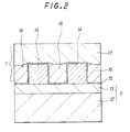
- a base or main body 11 comprises a semiconductor substrate 12, for example, on which a lower dielectric layer 13 consisting of silicon oxide (e.g., having a relative dielectric constant of 4.0) is formed.
- a lower dielectric layer 13 consisting of silicon oxide (e.g., having a relative dielectric constant of 4.0) is formed.
- a plurality of conductive interconnects 14 are formed over the lower dielectric layer 13 of the base 11.
- a first dielectric film 15 is formed so as to cover the conductive interconnects 14.
- This first dielectric film 15 is made of silicon oxide (e.g., having a relative dielectric constant of 4.0) having a film thickness of 2 nm.
- the film is made of silicon oxynitride (e.g., having a relative dielectric constant of 4.0-6.0) or silicon nitride (e.g., having a relative dielectric constant of 6.0).
- a second dielectric film 16 having a relative dielectric constant smaller than that of the first dielectric film 15 is formed between the conductive interconnects 14 via the first dielectric film 15. Also, the second dielectric film 16 is formed over the lower dielectric layer 13 which is on one side of the conductive interconnects 14. In the present figure, the second dielectric film 16 is formed over the lower dielectric layer 13 via the first dielectric film 15 but the second dielectric film 16 may be formed directly on the lower dielectric layer 13. That is, it is only necessary that the first dielectric layer 15 be present at least between each conductive interconnect 14 and the second dielectric film 16.
- the aforementioned second dielectric film 16 may be made of polysiloxane based polymer (e.g., having a relative dielectric constant of 2.8).
- the film may be made of silicon oxide containing fluorine atoms (e.g., having a relative dielectric constant of 3.0) or polyimide consisting of a polyimide material (e.g., having a relative dielectric constant of 3.0), or other suitable materials of low relative dielectric constant.
- An upper dielectric layer 17 consisting, for example, of silicon oxide (e.g., having a relative dielectric constant of 4.0) is formed over the first and second dielectric films 15 and 16, respectively.
- the interlayer dielectric film 1 is formed by the first and second dielectric films 15 and 16, respectively, and by the upper dielectric layer 17 so as to cover the conductive interconnects 14.
- the conductive interconnects 14 are formed over the semiconductor substrate 12 by ordinary conductive interconnect formation techniques.
- the lower dielectric layer 13 is formed on the front surface of the substrate 12.
- the first dielectric film 15 is formed over the lower dielectric layer 13 so as to cover the surfaces of the conductive interconnects 14, for example, by ECR (electron cyclotron resonance) CVD.
- silane (SiH4) and nitrous oxide (N2O) are used as reactant gases.
- Nitrogen (N2) is used as a carrier gas.
- the RF power is set to 500 W.
- the substrate temperature is set to 400°C.
- a polysiloxane based polymer is applied to form the second dielectric film 16.
- the second dielectric film 16 is etched back, for example by ECR etching, until the first dielectric film 15 over the conductive interconnects 14 is exposed.
- the second dielectric film 16 exists at least between the conductive interconnects 14.
- the upper dielectric layer 17 is formed out of silicon oxide over the first and second dielectric films 15 and 16, respectively, by CVD.
- the first dielectric film 15 is formed so as to cover the conductive interconnects 14 and so the interconnects 14 are protected from corrosion and poisoned vias due to the second dielectric film of low dielectric constant. Furthermore, since the second dielectric film 16 of a relative dielectric constant lower than that of the first dielectric film 15 is formed at least between the conductive interconnects 14, the electric field set up by the conductive interconnects passes through the second dielectric film 16 of low dielectric constant. Therefore, the capacitance between the conductive interconnects 14 is reduced.
- this interlayer dielectric film structure is similar to the structure shown in Fig. 2 except that the thickness of the second dielectric film 16 is larger than the height of the conductive interconnects 14 by 10-100% in the directions of the height and depth. That is, of the thickness di of the second dielectric film 16, the thickness dh of the portion higher than the conductive interconnects 14 and the thickness dl of the portion lower than the conductive interconnects 14 are set to 10-100% of the height D of the conductive interconnects 14.
- the base or main body 11 consists of the semiconductor substrate 12 having the lower dielectric layer 13 formed on its surface.
- the first dielectric film 15 is formed so as to cover the conductive interconnects 14.
- the upper dielectric layer 17 is formed over the first and second dielectric films 15 and 16, respectively.
- the method of fabrication of the interlayer dielectric film structure of the above-described second example is carried out by the same process as described in the first example.
- the difference with the process of the first example is that when the conductive interconnects 14 are patterned by etching, the lower dielectric layer 13 is also etched.
- the etching depth of the lower dielectric layer 13 is determined in the manner described below. Let de be the etching depth of the lower dielectric layer 13. Let dl be the thickness of the first dielectric film 15 which will be deposited later over the etched portions in the lower dielectric layer 13. Let D be the height of the conductive interconnects 14.
- ECR (electron cyclotron resonance) CVD is used to form the first dielectric film 15.
- the first dielectric film 15 is deposited over the etched portions in the lower dielectric layer 13 and over the conductive interconnects 14 to a thickness larger than side walls of the conductive interconnects 14.
- the thickness of the second dielectric film 16 between the conductive interconnects 14 is larger than the height D of the conductive interconnects 14 by 10-100% in the directions of the height and depth. Therefore, the capacitance between the conductive interconnects 14 is made lower than in the first example, because the electric field generated by the conductive interconnects 14 can pass more easily.
- the thickness amount is set to the above-described range.
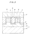
- this interlayer dielectric film structure is similar to the structure shown in Fig. 2 except that a third dielectric film 21 and a fourth dielectric film 22 are formed under the conductive interconnects 14.
- This third dielectric film 21 has substantially the same relative dielectric constant as the first dielectric film. Examples of the material include silicon oxide, silicon oxynitride, and silicon nitride.
- the thickness of the fourth dielectric film 22 is more than 10% and less than 30% of the height of the conductive interconnects 14.
- the fourth dielectric film 22 has substantially the same relative dielectric constant as the second dielectric film 16 as described previously in the first example.
- This fourth dielectric film 22 consists of at least one of silicon oxide containing fluorine, polysiloxane materials, polyparaxylylene, fluorocarbon materials, and polyimide materials.
- the base or main body 11 consists of the semiconductor substrate 12 having the lower dielectric layer 13 formed on its surface.
- the conductive interconnects 14 are formed over the lower dielectric layer 13 via the fourth and third dielectric films 22, 21, respectively.
- the first dielectric film 15 is formed so as to cover the conductive interconnects 14.
- the upper dielectric layer 17 is formed over the first and second dielectric films 15, 16.
- the interlayer dielectric film 1 is constructed in this way.
- the first dielectric film 15 and the third dielectric film 21 between the conductive interconnects 14 may be formed so as to surround the conductive interconnects 14.
- the method of fabrication of the interlayer dielectric film structure of the above-described third example is carried out by a process similar to the process previously described in the first example.
- the difference with the process of the first example is that the fourth dielectric film 22 and the third dielectric film 21 are successively stacked over the lower dielectric layer 13 before the conductive interconnects 14 are formed.
- the fourth dielectric film 22 is applied over the lower dielectric layer 13 to a film thickness of 100 nm.
- the third dielectric film 21 is formed to a film thickness, for example, of 10 nm by ECR CVD.
- the conductive interconnects 14 are formed by metallization formation techniques, followed by execution of the process already described in the first example.
- inter-layer dielectric film structure of the third example by a different process. This process is characterized in that the first and fourth dielectric films on that portion of the fourth dielectric film which is between the conductive interconnects are removed.
- a fourth dielectric film 22 is formed over the lower dielectric layer 13 of the base 11, for example, to a film thickness of 100 nm by an application method. Then, a third dielectric film 21 is formed, for example, to a film thickness of 10 nm by ECR CVD. Subsequently, a metallization film 31 for forming the conductive interconnects 14 are formed by sputtering. Then, a dielectric film 32 (which, in the finished product, is the first dielectric film 15) is formed on the metallization film 31 by CVD.
- a patterning step using ordinary lithography and etching techniques is carried out to form the conductive interconnects 14 from the metallization film 31 as shown in Fig. 5(b).
- the dielectric film 32 (later becoming the first dielectric film 15) is left over the conductive interconnects 14.
- the third dielectric film 21 at positions between the conductive interconnects 14 is etched away.
- side walls 33 (becoming the first dielectric film 15) are formed on the side walls of the conductive interconnects 14 by ordinary side wall formation techniques making use of formation of a further dielectric film (not shown) for the side walls and etch-back.
- the further dielectric film lying between the conductive interconnects 14 is removed during the etch-back for forming the side walls 33.
- the further dielectric film overlying the conductive interconnects 14 and used for the side walls is also removed.
- at least the bottom portion of the dielectric film 32 remains. Therefore, the conductive interconnects 14 are covered with the first dielectric film 15 consisting of the dielectric film 32 left on the conductive interconnects 14 and the side walls 33.
- the second dielectric film 16 is directly connected with the fourth dielectric film 22.
- the third dielectric film 21 and the fourth dielectric film 22 are formed under the conductive interconnects 14 and so the third dielectric film 21 having substantially the same relative dielectric constant as the first dielectric film 15 protects the conductive interconnects 14 from corrosion and poisoned vias due to the fourth dielectric film 22 of low dielectric constant. Because the thickness of the fourth dielectric film 22 is more than 10% and less than 30% of the height of the conductive interconnects 14, and because the fourth dielectric film 22 has substantially the same relative dielectric constant as the second dielectric film 16, the electric field produced by the conductive interconnects 14 passes through the fourth dielectric film 22 of low dielectric constant. Consequently, the capacitance between the conductive interconnects 14 is reduced.
- the thickness of the fourth dielectric film 22 is lower than 10% of the height of the conductive interconnects 14, the electric field developed by the conductive interconnects 14 hardly passes through the fourth dielectric film 22 but passes through the lower dielectric layer 13. Consequently, the capacitance is reduced less efficiently.
- the thickness is in excess of 30%, the moisture resistance is adversely affected, because the film quality of the fourth dielectric film 22 is poor.
- the film thickness of the fourth dielectric film 22 is set to the above-described range.
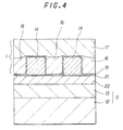
- this interlayer dielectric film structure is similar to the structure shown in Fig. 2 except that a fifth dielectric film 23 is formed over the conductive interconnects 14 via the first dielectric film 15.
- the fifth dielectric film 23 is formed also over the second dielectric film 16.
- the thickness of the fifth dielectric film 23 is more than 10% and less than 30% of the height of the conductive interconnects 14.
- the fifth dielectric film 23 has substantially the same relative dielectric constant as the second dielectric film 16 described in the first example.
- the fifth dielectric film 23 consists, for example, of at least one of silicon oxide containing fluorine, polysiloxane materials, polyparaxylylene, fluorocarbon materials, and polyimide materials.
- the fifth dielectric film 23 is formed to a film thickness of 100 nm, for example. In this case, it accounts for about 17% of the film thickness of the conductive interconnects 14.
- the structure is the same as the structure described already in connection with Fig. 2 in other respects.
- the base or main body 11 consists of the semiconductor substrate 12 having the lower dielectric layer 13 formed on its surface.
- the conductive interconnects 14 are formed over the lower dielectric layer 13.
- the first dielectric film 15 is formed so as to cover the conductive interconnects 14.
- the upper dielectric layer 17 is formed over the first and second dielectric films 15, 16, respectively, via the fifth dielectric layer 23.
- the interlayer dielectric film 1 is constructed in this way.
- the method of fabrication of the interlayer dielectric film structure of the above-described fourth example is carried out by a process similar to the process described in the first example.
- the difference with the process of the first example is that the second dielectric film 16 is left over the conductive interconnects 14 via the first dielectric film 15 when the second dielectric film 16 is etched back. That is, the second dielectric film 16 is left up to a thickness which is more than 10% and less than 30% of the height of the conductive interconnects 14.
- the left second dielectric film 16 becomes the fifth dielectric film 23. Therefore, the fifth dielectric film 23 consists of a polysiloxane based polymer, in the same way as the second dielectric film 16.
- the fifth film is made of silicon oxide containing fluorine carbon, poly-paraxylylene, a fluorocarbon material, or a polyimide material such as polyimide.
- the fifth dielectric film 23 is formed over the conductive interconnects 14 via the first dielectric film 15 and so the conductive interconnects 14 are protected from corrosion and poisoned vias due to the fifth dielectric film 23 of low dielectric constant. Because the thickness of the height of the conductive interconnects is more than 10% and less than 30% of the height of the conductive interconnects, and because the fifth dielectric film 23 having substantially the same relative dielectric constant as the second dielectric film 16 is formed, the electric field generated by the conductive interconnects 14 passes through the fifth dielectric film 23 of low dielectric constant. In consequence, the capacitance between the conductive interconnects 14 is reduced.
- the film thickness of the fifth dielectric film 23 is lower than 10% of the height of the conductive interconnects 14, the electric field developed by the conductive interconnects 14 hardly passes through the fifth dielectric film 23 but passes through the upper dielectric layer 17. Consequently, the capacitance is reduced less efficiently.
- the thickness is in excess of 30%, the moisture resistance is adversely affected, because the film quality of the fifth dielectric film 23 is poor.
- the film thickness is set to the above-described range.
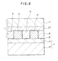
- FIG. 7 A fifth example which is a combination of the third example and the fourth example described above is next described by referring to the schematic cross section of Fig. 7.
- those components which are the same as their counterparts of Figs. 4 and 6 are indicated by the same reference numerals.
- this interlayer dielectric film structure combines the structure shown in Fig. 4 with the structure shown in Fig. 6. That is, a fourth dielectric film 22 and a third dielectric film 21 are formed over the lower dielectric layer 13 of the base 11. Conductive interconnects 14 are formed over the third dielectric film 21. Therefore, the third dielectric film 21 and the fourth dielectric film 22 are formed under the conductive interconnects 14.
- the third dielectric film 21 is made of a material having substantially the same relative dielectric constant as the first dielectric film 15, e.g., silicon oxide, silicon oxynitride, or silicon nitride.
- the thickness of the fourth dielectric film 22 is more than 10% and less than 30% of the height of the conductive interconnects 14.
- the fourth dielectric film 22 has substantially the same relative dielectric constant as the second dielectric film 16 described in the first example.
- This fourth dielectric film 22 consists, for example, of at least one of silicon oxide containing fluorine, polysiloxane materials, polyparaxylylene, fluorocarbon materials, and polyimide materials.
- the conductive interconnects 14 are coated with the first dielectric film 15.
- the second dielectric film 16 similar to that described in the first example is formed between the conductive interconnects 14 via the first dielectric film 15 similar to that described in the first example.
- a fifth dielectric film 23 is formed over the conductive interconnects 14 via the first dielectric film 15. This fifth dielectric film 23 is formed also over the second dielectric film 16.
- the thickness of the fifth dielectric film 23 is more than 10% and less than 30% of the height of the conductive interconnects 14.
- the fifth dielectric film 23 has substantially the same relative dielectric constant as the second dielectric film 16.
- This fifth dielectric film 23 consists, for example, of at least one of silicon oxide containing fluorine, polysiloxane materials, polyparaxylylene, fluorocarbon materials, and polyimide materials.
- the upper dielectric layer 17 consisting, for example, of silicon oxide is formed over the fifth dielectric film 23.
- the interlayer dielectric film 1 is constructed in this way.
- the third dielectric film 21 is formed to a film thickness of 10 nm, for example.
- the fourth dielectric film 22 is formed to a film thickness of 100 nm.
- the fifth dielectric film 23 is formed to a film thickness of 100 nm. In this case, the film thicknesses of the fourth and fifth dielectric films 22 and 23 account for about 17% of the film thickness of the conductive interconnects 14.
- the fourth dielectric film 22, the third dielectric film 21, and the conductive interconnects 14 are formed by a process similar to the process described in the third example. Then, the first dielectric film 15 is formed. Thereafter, the second dielectric film 16 and the fifth dielectric film 23 are formed integrally by a process similar to the process described in the fourth example. Subsequently, the upper dielectric layer 17 is formed.
- the fourth dielectric film 22 is formed under the conductive interconnects 14 via the third dielectric film 21.
- the second dielectric film 16 is formed over the conductive interconnects 14 via the first dielectric film 15. Consequently, the capacitance between the conductive interconnects 14 is made lower than in the third and fourth examples.
- FIG. 8(a) illustrates an interlayer dielectric film structure according to the prior art.
- those components which are the same as their counterparts of the above examples are indicated by the same reference numerals.
- Fig. 8(b) illustrates the manner in which the jut-out ratio of the low dielectric constant body in an interlayer dielectric film structure according to the invention is found.
- those components which are the same as their counterparts of the above examples are indicated by the same reference numerals. Plotted on the vertical axis of Fig.
- a plurality of conductive interconnects 14 are formed to a thickness of 600 nm over the lower dielectric layer 13 made of silicon oxide and having a relative dielectric constant of 4.0.
- a silicon oxide film 31 having a thickness of 200 nm and a relative dielectric constant of 4.0 is formed over the conductive interconnects 14.
- the lower dielectric layers 13 which are located on both sides and over which the conductive interconnects 14 are formed are lower by 200 nm than those portions in which the conductive interconnects 14 are formed.
- the second dielectric film 16 consisting of a low dielectric constant substance polyimide (relative dielectric constant is approximately equal to 3.0) is formed on both sides of the conductive interconnects 14 and the silicon oxide film 31.
- the upper dielectric layer 17 having a relative dielectric constant of 4.0 is formed over the silicon oxide film 31 and over the second dielectric film 16.
- the upper dielectric layer 17 is formed by plasma CVD, using tetraethoxysilane as a raw material. In this way, an interlayer dielectric film is formed by the second dielectric film 16, the silicon oxide film 31, and the upper dielectric film 17.
- the conductive interconnects 14 having a height of b are formed over the lower dielectric layer 13 having a relative dielectric constant of 4.0.
- the second dielectric film 16 consisting of a low dielectric substance and having a height of a is formed between the conductive interconnects 14.
- the upper dielectric layer 17 having a relative dielectric constant of 4.0 is formed over the conductive interconnects 14 and over the second dielectric film 16.
- the first dielectric film described in the above examples is not shown in this figure.
- the calculated film thickness of the second dielectric film includes the film thicknesses of the fourth and fifth dielectric films.
- the jut-out ratio R is in the range from 0.1 to 0.3. This shows that the capacitance between the conductive interconnects is reduced by at least 4-7% compared with the prior art structure.
- the reduction ratio of the converted capacitance between the conductive interconnects of the third and fourth examples described above is about half the reduction ratio of the converted capacitance of the fifth example.
- Fig. 9 An example in which the fifth example of the invention is applied to an ordinary polycide gate MOS transistor is described by referring to Fig. 9.
- Fig. 9 the structure of Fig. 9 is compared with the structure of Fig. 7 which is a schematic cross section of the fifth example of the invention.
- the polycide gate MOS transistor corresponds to the semiconductor substrate 12 shown in Fig. 7.
- the method of fabricating the polycide gate MOS transistor is not described herein.
- the silicon oxide film 13 formed on the surface of the polycide gate MOS transistor corresponds to the lower oxide film 13 shown in Fig. 7.
- the fourth dielectric film 22 of a low dielectric constant is formed on the silicon oxide film 13.
- the third dielectric film 21 is formed on the fourth dielectric film 22.
- aluminum is deposited. This aluminum film is patterned, making use of a photolithography step and an etching step. Thus, the conductive interconnects 14 are formed.
- the first dielectric film 15 is formed and the second dielectric film 16 is buried on the principle of the fifth example of the invention. This is followed by formation of the fifth dielectric film 23 and the upper dielectric layer 17. The manner in which these films are formed has been already described in the fifth example.
Landscapes
- Engineering & Computer Science (AREA)
- Physics & Mathematics (AREA)
- Condensed Matter Physics & Semiconductors (AREA)
- General Physics & Mathematics (AREA)
- Computer Hardware Design (AREA)
- Microelectronics & Electronic Packaging (AREA)
- Power Engineering (AREA)
- Manufacturing & Machinery (AREA)
- Internal Circuitry In Semiconductor Integrated Circuit Devices (AREA)
Applications Claiming Priority (4)
| Application Number | Priority Date | Filing Date | Title |
|---|---|---|---|
| JP238821/94 | 1994-10-03 | ||
| JP23882194 | 1994-10-03 | ||
| JP3727/95 | 1995-01-13 | ||
| JP7003727A JPH08162528A (ja) | 1994-10-03 | 1995-01-13 | 半導体装置の層間絶縁膜構造 |
Publications (3)
| Publication Number | Publication Date |
|---|---|
| EP0706216A2 true EP0706216A2 (fr) | 1996-04-10 |
| EP0706216A3 EP0706216A3 (fr) | 1997-12-03 |
| EP0706216B1 EP0706216B1 (fr) | 2007-05-30 |
Family
ID=26337363
Family Applications (1)
| Application Number | Title | Priority Date | Filing Date |
|---|---|---|---|
| EP95402206A Expired - Lifetime EP0706216B1 (fr) | 1994-10-03 | 1995-10-03 | Couche intermédiaire diélectrique pour un dispositif semi-conducteur |
Country Status (5)
| Country | Link |
|---|---|
| US (1) | US5646440A (fr) |
| EP (1) | EP0706216B1 (fr) |
| JP (1) | JPH08162528A (fr) |
| KR (1) | KR960015788A (fr) |
| DE (1) | DE69535502T2 (fr) |
Cited By (36)
| Publication number | Priority date | Publication date | Assignee | Title |
|---|---|---|---|---|
| FR2741192A1 (fr) * | 1995-11-10 | 1997-05-16 | Samsung Electronics Co Ltd | Procede de conception et de fabrication de circuits integres et circuits integres realises selon ce procede |
| EP0805491A2 (fr) * | 1996-04-29 | 1997-11-05 | Texas Instruments Incorporated | Structure d'interconnexion et méthode de fabrication utilisant deux isolants différents avec une faible constante diélectrique |
| WO1997041592A1 (fr) * | 1996-05-02 | 1997-11-06 | Advanced Micro Devices, Inc. | Couches superposees dielectriques a faible permittivite constituees d'oxyde fluore pour couplage capacitif reduit |
| EP0851491A2 (fr) * | 1996-12-25 | 1998-07-01 | Nec Corporation | Composant semiconducteur comprenant des interconnections multicouches et sa méthode de fabrication |
| EP0851490A2 (fr) * | 1996-12-25 | 1998-07-01 | Nec Corporation | Dispositif semi-conducteur et procédé pour fabriquer celui-ci |
| EP1094508A2 (fr) | 1999-10-22 | 2001-04-25 | Lsi Logic Corporation | Couche diélectrique composite sans cavités de faible constante diélectrique pour structures de circuits intégrés |
| EP1123991A2 (fr) * | 2000-02-08 | 2001-08-16 | Asm Japan K.K. | Matériaux à faible constante diélectrique et procédés |
| US6346488B1 (en) | 2000-06-27 | 2002-02-12 | Lsi Logic Corporation | Process to provide enhanced resistance to cracking and to further reduce the dielectric constant of a low dielectric constant dielectric film of an integrated circuit structure by implantation with hydrogen ions |
| US6346490B1 (en) | 2000-04-05 | 2002-02-12 | Lsi Logic Corporation | Process for treating damaged surfaces of low k carbon doped silicon oxide dielectric material after plasma etching and plasma cleaning steps |
| US6350700B1 (en) | 2000-06-28 | 2002-02-26 | Lsi Logic Corporation | Process for forming trenches and vias in layers of low dielectric constant carbon-doped silicon oxide dielectric material of an integrated circuit structure |
| US6365528B1 (en) | 2000-06-07 | 2002-04-02 | Lsi Logic Corporation | Low temperature process for forming a low dielectric constant fluorine and carbon-containing silicon oxide dielectric-material characterized by improved resistance to oxidation and good gap-filling capabilities |
| US6368979B1 (en) | 2000-06-28 | 2002-04-09 | Lsi Logic Corporation | Process for forming trenches and vias in layers of low dielectric constant carbon-doped silicon oxide dielectric material of an integrated circuit structure |
| US6391768B1 (en) | 2000-10-30 | 2002-05-21 | Lsi Logic Corporation | Process for CMP removal of excess trench or via filler metal which inhibits formation of concave regions on oxide surface of integrated circuit structure |
| US6420277B1 (en) | 2000-11-01 | 2002-07-16 | Lsi Logic Corporation | Process for inhibiting crack formation in low dielectric constant dielectric films of integrated circuit structure |
| US6423628B1 (en) | 1999-10-22 | 2002-07-23 | Lsi Logic Corporation | Method of forming integrated circuit structure having low dielectric constant material and having silicon oxynitride caps over closely spaced apart metal lines |
| US6444564B1 (en) | 1998-11-23 | 2002-09-03 | Advanced Micro Devices, Inc. | Method and product for improved use of low k dielectric material among integrated circuit interconnect structures |
| US6489242B1 (en) | 2000-09-13 | 2002-12-03 | Lsi Logic Corporation | Process for planarization of integrated circuit structure which inhibits cracking of low dielectric constant dielectric material adjacent underlying raised structures |
| US6492731B1 (en) | 2000-06-27 | 2002-12-10 | Lsi Logic Corporation | Composite low dielectric constant film for integrated circuit structure |
| US6503840B2 (en) | 2001-05-02 | 2003-01-07 | Lsi Logic Corporation | Process for forming metal-filled openings in low dielectric constant dielectric material while inhibiting via poisoning |
| US6524974B1 (en) | 1999-03-22 | 2003-02-25 | Lsi Logic Corporation | Formation of improved low dielectric constant carbon-containing silicon oxide dielectric material by reaction of carbon-containing silane with oxidizing agent in the presence of one or more reaction retardants |
| US6537923B1 (en) | 2000-10-31 | 2003-03-25 | Lsi Logic Corporation | Process for forming integrated circuit structure with low dielectric constant material between closely spaced apart metal lines |
| US6559048B1 (en) | 2001-05-30 | 2003-05-06 | Lsi Logic Corporation | Method of making a sloped sidewall via for integrated circuit structure to suppress via poisoning |
| US6559033B1 (en) | 2001-06-27 | 2003-05-06 | Lsi Logic Corporation | Processing for forming integrated circuit structure with low dielectric constant material between closely spaced apart metal lines |
| US6562700B1 (en) | 2001-05-31 | 2003-05-13 | Lsi Logic Corporation | Process for removal of resist mask over low k carbon-doped silicon oxide dielectric material of an integrated circuit structure, and removal of residues from via etch and resist mask removal |
| US6566171B1 (en) | 2001-06-12 | 2003-05-20 | Lsi Logic Corporation | Fuse construction for integrated circuit structure having low dielectric constant dielectric material |
| US6572925B2 (en) | 2001-02-23 | 2003-06-03 | Lsi Logic Corporation | Process for forming a low dielectric constant fluorine and carbon containing silicon oxide dielectric material |
| US6583026B1 (en) | 2001-05-31 | 2003-06-24 | Lsi Logic Corporation | Process for forming a low k carbon-doped silicon oxide dielectric material on an integrated circuit structure |
| EP1325280A1 (fr) * | 2000-09-14 | 2003-07-09 | Conexant Systems, Inc. | Procede et structure de stabilisation de la temperature dans des dispositifs a semi-conducteurs |
| US6649219B2 (en) | 2001-02-23 | 2003-11-18 | Lsi Logic Corporation | Process for forming a low dielectric constant fluorine and carbon-containing silicon oxide dielectric material characterized by improved resistance to oxidation |
| US6673721B1 (en) | 2001-07-02 | 2004-01-06 | Lsi Logic Corporation | Process for removal of photoresist mask used for making vias in low k carbon-doped silicon oxide dielectric material, and for removal of etch residues from formation of vias and removal of photoresist mask |
| US6723653B1 (en) | 2001-08-17 | 2004-04-20 | Lsi Logic Corporation | Process for reducing defects in copper-filled vias and/or trenches formed in porous low-k dielectric material |
| US6756674B1 (en) | 1999-10-22 | 2004-06-29 | Lsi Logic Corporation | Low dielectric constant silicon oxide-based dielectric layer for integrated circuit structures having improved compatibility with via filler materials, and method of making same |
| US6790784B2 (en) | 2001-06-19 | 2004-09-14 | Lsi Logic Corporation | Plasma treatment of low dielectric constant dielectric material to form structures useful in formation of metal interconnects and/or filled vias for intergrated circuit structure |
| US6858195B2 (en) | 2001-02-23 | 2005-02-22 | Lsi Logic Corporation | Process for forming a low dielectric constant fluorine and carbon-containing silicon oxide dielectric material |
| US6881664B2 (en) | 2001-08-28 | 2005-04-19 | Lsi Logic Corporation | Process for planarizing upper surface of damascene wiring structure for integrated circuit structures |
| US6905981B1 (en) | 2000-11-24 | 2005-06-14 | Asm Japan K.K. | Low-k dielectric materials and processes |
Families Citing this family (20)
| Publication number | Priority date | Publication date | Assignee | Title |
|---|---|---|---|---|
| JPH0936226A (ja) * | 1995-07-18 | 1997-02-07 | Nec Corp | 半導体装置およびその製造方法 |
| US6157083A (en) * | 1996-06-03 | 2000-12-05 | Nec Corporation | Fluorine doping concentrations in a multi-structure semiconductor device |
| US5843830A (en) * | 1996-06-26 | 1998-12-01 | Micron Technology, Inc. | Capacitor, and methods for forming a capacitor |
| JP2910713B2 (ja) | 1996-12-25 | 1999-06-23 | 日本電気株式会社 | 半導体装置の製造方法 |
| US6437441B1 (en) | 1997-07-10 | 2002-08-20 | Kawasaki Microelectronics, Inc. | Wiring structure of a semiconductor integrated circuit and a method of forming the wiring structure |
| JP3305251B2 (ja) | 1998-02-26 | 2002-07-22 | 松下電器産業株式会社 | 配線構造体の形成方法 |
| JP3123512B2 (ja) * | 1998-06-02 | 2001-01-15 | 日本電気株式会社 | 半導体装置及びその製造方法 |
| US6232235B1 (en) | 1998-06-03 | 2001-05-15 | Motorola, Inc. | Method of forming a semiconductor device |
| US6265779B1 (en) * | 1998-08-11 | 2001-07-24 | International Business Machines Corporation | Method and material for integration of fuorine-containing low-k dielectrics |
| US6239026B1 (en) | 1998-09-28 | 2001-05-29 | Conexant Systems, Inc. | Nitride etch stop for poisoned unlanded vias |
| US6777320B1 (en) * | 1998-11-13 | 2004-08-17 | Intel Corporation | In-plane on-chip decoupling capacitors and method for making same |
| US6080683A (en) * | 1999-03-22 | 2000-06-27 | Special Materials Research And Technology, Inc. | Room temperature wet chemical growth process of SiO based oxides on silicon |
| US6593077B2 (en) | 1999-03-22 | 2003-07-15 | Special Materials Research And Technology, Inc. | Method of making thin films dielectrics using a process for room temperature wet chemical growth of SiO based oxides on a substrate |
| JP2000286262A (ja) * | 1999-03-30 | 2000-10-13 | Mitsubishi Electric Corp | 半導体装置及びその製造方法 |
| JP2007281513A (ja) * | 1999-06-25 | 2007-10-25 | Toshiba Corp | Lsiの配線構造 |
| US6774489B2 (en) * | 2000-08-29 | 2004-08-10 | Texas Instruments Incorporated | Dielectric layer liner for an integrated circuit structure |
| US6613697B1 (en) | 2001-06-26 | 2003-09-02 | Special Materials Research And Technology, Inc. | Low metallic impurity SiO based thin film dielectrics on semiconductor substrates using a room temperature wet chemical growth process, method and applications thereof |
| RU2218365C2 (ru) * | 2001-07-27 | 2003-12-10 | Федеральное государственное унитарное предприятие "Научно-исследовательский физико-химический институт им. Л.Я.Карпова" | Пористая пленка из полипараксилилена и его замещенных, способ ее получения и полупроводниковый прибор с её использованием |
| US6762494B1 (en) * | 2002-09-24 | 2004-07-13 | Applied Micro Circuits Corporation | Electronic package substrate with an upper dielectric layer covering high speed signal traces |
| JP2004128256A (ja) | 2002-10-03 | 2004-04-22 | Oki Electric Ind Co Ltd | 多層構造半導体素子の製造方法 |
Citations (1)
| Publication number | Priority date | Publication date | Assignee | Title |
|---|---|---|---|---|
| JPS637650A (ja) | 1986-06-27 | 1988-01-13 | Nippon Telegr & Teleph Corp <Ntt> | 半導体集積回路の配線構造 |
Family Cites Families (13)
| Publication number | Priority date | Publication date | Assignee | Title |
|---|---|---|---|---|
| JPS56150830A (en) * | 1980-04-25 | 1981-11-21 | Hitachi Ltd | Semiconductor device |
| JPS56167333A (en) * | 1980-05-26 | 1981-12-23 | Fujitsu Ltd | Semiconductor device |
| JPH0612790B2 (ja) * | 1987-02-24 | 1994-02-16 | 日本電気株式会社 | 半導体装置 |
| JPH0654774B2 (ja) * | 1987-11-30 | 1994-07-20 | 株式会社東芝 | 半導体装置及びその製造方法 |
| JPH0230138A (ja) * | 1988-07-19 | 1990-01-31 | Seiko Epson Corp | 半導体装置 |
| JPH0289346A (ja) * | 1988-09-27 | 1990-03-29 | Toshiba Corp | 半導体装置及びその製造方法 |
| NL8900989A (nl) * | 1989-04-20 | 1990-11-16 | Philips Nv | Halfgeleiderinrichting met een in een kunststof omhulling ingebed halfgeleiderlichaam. |
| JPH04174541A (ja) * | 1990-03-28 | 1992-06-22 | Nec Corp | 半導体集積回路及びその製造方法 |
| JPH04147651A (ja) * | 1990-04-02 | 1992-05-21 | Toshiba Corp | 半導体装置およびその製造方法 |
| JP2593965B2 (ja) * | 1991-01-29 | 1997-03-26 | 三菱電機株式会社 | 半導体装置 |
| JPH04323854A (ja) * | 1991-04-23 | 1992-11-13 | Oki Electric Ind Co Ltd | 半導体装置 |
| JPH05283542A (ja) * | 1992-03-31 | 1993-10-29 | Mitsubishi Electric Corp | 半導体集積回路装置及びその製造方法 |
| KR0131439B1 (ko) * | 1992-11-24 | 1998-04-14 | 나카무라 타메아키 | 반도체장치 및 그 제조방법 |
-
1995
- 1995-01-13 JP JP7003727A patent/JPH08162528A/ja active Pending
- 1995-09-27 US US08/534,405 patent/US5646440A/en not_active Expired - Lifetime
- 1995-10-02 KR KR1019950033748A patent/KR960015788A/ko not_active Application Discontinuation
- 1995-10-03 DE DE69535502T patent/DE69535502T2/de not_active Expired - Fee Related
- 1995-10-03 EP EP95402206A patent/EP0706216B1/fr not_active Expired - Lifetime
Patent Citations (1)
| Publication number | Priority date | Publication date | Assignee | Title |
|---|---|---|---|---|
| JPS637650A (ja) | 1986-06-27 | 1988-01-13 | Nippon Telegr & Teleph Corp <Ntt> | 半導体集積回路の配線構造 |
Cited By (52)
| Publication number | Priority date | Publication date | Assignee | Title |
|---|---|---|---|---|
| FR2741192A1 (fr) * | 1995-11-10 | 1997-05-16 | Samsung Electronics Co Ltd | Procede de conception et de fabrication de circuits integres et circuits integres realises selon ce procede |
| EP0805491A2 (fr) * | 1996-04-29 | 1997-11-05 | Texas Instruments Incorporated | Structure d'interconnexion et méthode de fabrication utilisant deux isolants différents avec une faible constante diélectrique |
| EP0805491A3 (fr) * | 1996-04-29 | 1997-11-12 | Texas Instruments Incorporated | Structure d'interconnexion et méthode de fabrication utilisant deux isolants différents avec une faible constante diélectrique |
| WO1997041592A1 (fr) * | 1996-05-02 | 1997-11-06 | Advanced Micro Devices, Inc. | Couches superposees dielectriques a faible permittivite constituees d'oxyde fluore pour couplage capacitif reduit |
| EP0851491A2 (fr) * | 1996-12-25 | 1998-07-01 | Nec Corporation | Composant semiconducteur comprenant des interconnections multicouches et sa méthode de fabrication |
| EP0851490A2 (fr) * | 1996-12-25 | 1998-07-01 | Nec Corporation | Dispositif semi-conducteur et procédé pour fabriquer celui-ci |
| EP0851491A3 (fr) * | 1996-12-25 | 1998-08-19 | Nec Corporation | Composant semiconducteur comprenant des interconnections multicouches et sa méthode de fabrication |
| EP0851490A3 (fr) * | 1996-12-25 | 1999-12-22 | Nec Corporation | Dispositif semi-conducteur et procédé pour fabriquer celui-ci |
| US6498398B1 (en) | 1996-12-25 | 2002-12-24 | Nec Corporation | Semiconductor device having through holes selectively through isolation material covering wirings that are relatively far apart |
| US6444564B1 (en) | 1998-11-23 | 2002-09-03 | Advanced Micro Devices, Inc. | Method and product for improved use of low k dielectric material among integrated circuit interconnect structures |
| US6524974B1 (en) | 1999-03-22 | 2003-02-25 | Lsi Logic Corporation | Formation of improved low dielectric constant carbon-containing silicon oxide dielectric material by reaction of carbon-containing silane with oxidizing agent in the presence of one or more reaction retardants |
| US6800940B2 (en) | 1999-10-22 | 2004-10-05 | Lsi Logic Corporation | Low k dielectric composite layer for integrated circuit structure which provides void-free low k dielectric material between metal lines while mitigating via poisoning |
| US6756674B1 (en) | 1999-10-22 | 2004-06-29 | Lsi Logic Corporation | Low dielectric constant silicon oxide-based dielectric layer for integrated circuit structures having improved compatibility with via filler materials, and method of making same |
| US6423628B1 (en) | 1999-10-22 | 2002-07-23 | Lsi Logic Corporation | Method of forming integrated circuit structure having low dielectric constant material and having silicon oxynitride caps over closely spaced apart metal lines |
| EP1094508A3 (fr) * | 1999-10-22 | 2001-07-11 | Lsi Logic Corporation | Couche diélectrique composite sans cavités de faible constante diélectrique pour structures de circuits intégrés |
| EP1094508A2 (fr) | 1999-10-22 | 2001-04-25 | Lsi Logic Corporation | Couche diélectrique composite sans cavités de faible constante diélectrique pour structures de circuits intégrés |
| US7144620B2 (en) | 2000-02-08 | 2006-12-05 | Asm Japan K.K. | Process for depositing low dielectric constant materials |
| US7544827B2 (en) | 2000-02-08 | 2009-06-09 | Asm Japan K.K. | Process for depositing low dielectric constant materials |
| EP1123991A2 (fr) * | 2000-02-08 | 2001-08-16 | Asm Japan K.K. | Matériaux à faible constante diélectrique et procédés |
| US6733830B2 (en) | 2000-02-08 | 2004-05-11 | Asm Japan K.K. | Processes for depositing low dielectric constant materials |
| EP1123991A3 (fr) * | 2000-02-08 | 2002-11-13 | Asm Japan K.K. | Matériaux à faible constante diélectrique et procédés |
| US6346490B1 (en) | 2000-04-05 | 2002-02-12 | Lsi Logic Corporation | Process for treating damaged surfaces of low k carbon doped silicon oxide dielectric material after plasma etching and plasma cleaning steps |
| US6365528B1 (en) | 2000-06-07 | 2002-04-02 | Lsi Logic Corporation | Low temperature process for forming a low dielectric constant fluorine and carbon-containing silicon oxide dielectric-material characterized by improved resistance to oxidation and good gap-filling capabilities |
| US6346488B1 (en) | 2000-06-27 | 2002-02-12 | Lsi Logic Corporation | Process to provide enhanced resistance to cracking and to further reduce the dielectric constant of a low dielectric constant dielectric film of an integrated circuit structure by implantation with hydrogen ions |
| US6492731B1 (en) | 2000-06-27 | 2002-12-10 | Lsi Logic Corporation | Composite low dielectric constant film for integrated circuit structure |
| US6350700B1 (en) | 2000-06-28 | 2002-02-26 | Lsi Logic Corporation | Process for forming trenches and vias in layers of low dielectric constant carbon-doped silicon oxide dielectric material of an integrated circuit structure |
| US6368979B1 (en) | 2000-06-28 | 2002-04-09 | Lsi Logic Corporation | Process for forming trenches and vias in layers of low dielectric constant carbon-doped silicon oxide dielectric material of an integrated circuit structure |
| US6489242B1 (en) | 2000-09-13 | 2002-12-03 | Lsi Logic Corporation | Process for planarization of integrated circuit structure which inhibits cracking of low dielectric constant dielectric material adjacent underlying raised structures |
| US6713394B2 (en) | 2000-09-13 | 2004-03-30 | Lsi Logic Corporation | Process for planarization of integrated circuit structure which inhibits cracking of low dielectric constant dielectric material adjacent underlying raised structures |
| EP1325280A1 (fr) * | 2000-09-14 | 2003-07-09 | Conexant Systems, Inc. | Procede et structure de stabilisation de la temperature dans des dispositifs a semi-conducteurs |
| EP1325280A4 (fr) * | 2000-09-14 | 2006-10-04 | Skyworks Solutions Inc | Procede et structure de stabilisation de la temperature dans des dispositifs a semi-conducteurs |
| US6391768B1 (en) | 2000-10-30 | 2002-05-21 | Lsi Logic Corporation | Process for CMP removal of excess trench or via filler metal which inhibits formation of concave regions on oxide surface of integrated circuit structure |
| US6537923B1 (en) | 2000-10-31 | 2003-03-25 | Lsi Logic Corporation | Process for forming integrated circuit structure with low dielectric constant material between closely spaced apart metal lines |
| US6420277B1 (en) | 2000-11-01 | 2002-07-16 | Lsi Logic Corporation | Process for inhibiting crack formation in low dielectric constant dielectric films of integrated circuit structure |
| US6905981B1 (en) | 2000-11-24 | 2005-06-14 | Asm Japan K.K. | Low-k dielectric materials and processes |
| US7015168B2 (en) | 2001-02-23 | 2006-03-21 | Lsi Logic Corporation | Low dielectric constant fluorine and carbon-containing silicon oxide dielectric material characterized by improved resistance to oxidation |
| US6858195B2 (en) | 2001-02-23 | 2005-02-22 | Lsi Logic Corporation | Process for forming a low dielectric constant fluorine and carbon-containing silicon oxide dielectric material |
| US6572925B2 (en) | 2001-02-23 | 2003-06-03 | Lsi Logic Corporation | Process for forming a low dielectric constant fluorine and carbon containing silicon oxide dielectric material |
| US6649219B2 (en) | 2001-02-23 | 2003-11-18 | Lsi Logic Corporation | Process for forming a low dielectric constant fluorine and carbon-containing silicon oxide dielectric material characterized by improved resistance to oxidation |
| US6503840B2 (en) | 2001-05-02 | 2003-01-07 | Lsi Logic Corporation | Process for forming metal-filled openings in low dielectric constant dielectric material while inhibiting via poisoning |
| US6559048B1 (en) | 2001-05-30 | 2003-05-06 | Lsi Logic Corporation | Method of making a sloped sidewall via for integrated circuit structure to suppress via poisoning |
| US6583026B1 (en) | 2001-05-31 | 2003-06-24 | Lsi Logic Corporation | Process for forming a low k carbon-doped silicon oxide dielectric material on an integrated circuit structure |
| US6562700B1 (en) | 2001-05-31 | 2003-05-13 | Lsi Logic Corporation | Process for removal of resist mask over low k carbon-doped silicon oxide dielectric material of an integrated circuit structure, and removal of residues from via etch and resist mask removal |
| US6566171B1 (en) | 2001-06-12 | 2003-05-20 | Lsi Logic Corporation | Fuse construction for integrated circuit structure having low dielectric constant dielectric material |
| US6806551B2 (en) | 2001-06-12 | 2004-10-19 | Lsi Logic Corporation | Fuse construction for integrated circuit structure having low dielectric constant dielectric material |
| US6930056B1 (en) | 2001-06-19 | 2005-08-16 | Lsi Logic Corporation | Plasma treatment of low dielectric constant dielectric material to form structures useful in formation of metal interconnects and/or filled vias for integrated circuit structure |
| US6790784B2 (en) | 2001-06-19 | 2004-09-14 | Lsi Logic Corporation | Plasma treatment of low dielectric constant dielectric material to form structures useful in formation of metal interconnects and/or filled vias for intergrated circuit structure |
| US6559033B1 (en) | 2001-06-27 | 2003-05-06 | Lsi Logic Corporation | Processing for forming integrated circuit structure with low dielectric constant material between closely spaced apart metal lines |
| US6673721B1 (en) | 2001-07-02 | 2004-01-06 | Lsi Logic Corporation | Process for removal of photoresist mask used for making vias in low k carbon-doped silicon oxide dielectric material, and for removal of etch residues from formation of vias and removal of photoresist mask |
| US7071113B2 (en) | 2001-07-02 | 2006-07-04 | Lsi Logic Corporation | Process for removal of photoresist mask used for making vias in low K carbon-doped silicon oxide dielectric material, and for removal of etch residues from formation of vias and removal of photoresist mask |
| US6723653B1 (en) | 2001-08-17 | 2004-04-20 | Lsi Logic Corporation | Process for reducing defects in copper-filled vias and/or trenches formed in porous low-k dielectric material |
| US6881664B2 (en) | 2001-08-28 | 2005-04-19 | Lsi Logic Corporation | Process for planarizing upper surface of damascene wiring structure for integrated circuit structures |
Also Published As
| Publication number | Publication date |
|---|---|
| EP0706216B1 (fr) | 2007-05-30 |
| EP0706216A3 (fr) | 1997-12-03 |
| KR960015788A (ko) | 1996-05-22 |
| JPH08162528A (ja) | 1996-06-21 |
| DE69535502D1 (de) | 2007-07-12 |
| DE69535502T2 (de) | 2008-01-24 |
| US5646440A (en) | 1997-07-08 |
Similar Documents
| Publication | Publication Date | Title |
|---|---|---|
| EP0706216B1 (fr) | Couche intermédiaire diélectrique pour un dispositif semi-conducteur | |
| US6593659B2 (en) | Dual damascene structure with carbon containing SiO2 dielectric layers | |
| US6617244B2 (en) | Etching method | |
| US5945155A (en) | Low dielectric constant amorphous fluorinated carbon and method of preparation | |
| US5607773A (en) | Method of forming a multilevel dielectric | |
| US6162583A (en) | Method for making intermetal dielectrics (IMD) on semiconductor integrated circuits using low dielectric constant spin-on polymers | |
| US6566260B2 (en) | Non-metallic barrier formations for copper damascene type interconnects | |
| EP1122773B1 (fr) | Procédé de fabrication d'un dispositif semiconducteur | |
| KR100337580B1 (ko) | 반도체장치및그제조방법 | |
| KR100288827B1 (ko) | 반도체장치 및 그 제조방법 | |
| US6333558B1 (en) | Semiconductor device and method for fabricating the same | |
| US7304386B2 (en) | Semiconductor device having a multilayer wiring structure | |
| US6486559B1 (en) | Copper wiring structure comprising a copper material buried in a hollow of an insulating film and a carbon layer between the hollow and the copper material in semiconductor device and method of fabricating the same | |
| US6607986B2 (en) | Dry etching method and semiconductor device manufacturing method | |
| US6624061B2 (en) | Semiconductor device and method of manufacturing the same capable of reducing deterioration of low dielectric constant film | |
| US20060205201A1 (en) | Electric device and method for fabricating the same | |
| US6309958B1 (en) | Semiconductor device and method of manufacturing the same | |
| US5344797A (en) | Method of forming interlevel dielectric for integrated circuits | |
| US5231055A (en) | Method of forming composite interconnect system | |
| US5985749A (en) | Method of forming a via hole structure including CVD tungsten silicide barrier layer | |
| JP3435186B2 (ja) | 半導体装置 | |
| JPH09129727A (ja) | 半導体装置及びその製造方法 | |
| US6548900B1 (en) | Semiconductor device and fabrication method thereof | |
| KR100258044B1 (ko) | 반도체 장치 및 그 제조 방법 | |
| US20030015798A1 (en) | Semiconductor device and method of fabricating the semiconductor device |
Legal Events
| Date | Code | Title | Description |
|---|---|---|---|
| PUAI | Public reference made under article 153(3) epc to a published international application that has entered the european phase |
Free format text: ORIGINAL CODE: 0009012 |
|
| AK | Designated contracting states |
Kind code of ref document: A2 Designated state(s): DE FR GB |
|
| PUAL | Search report despatched |
Free format text: ORIGINAL CODE: 0009013 |
|
| AK | Designated contracting states |
Kind code of ref document: A3 Designated state(s): DE FR GB |
|
| 17P | Request for examination filed |
Effective date: 19980514 |
|
| 17Q | First examination report despatched |
Effective date: 20020801 |
|
| GRAP | Despatch of communication of intention to grant a patent |
Free format text: ORIGINAL CODE: EPIDOSNIGR1 |
|
| GRAC | Information related to communication of intention to grant a patent modified |
Free format text: ORIGINAL CODE: EPIDOSCIGR1 |
|
| GRAS | Grant fee paid |
Free format text: ORIGINAL CODE: EPIDOSNIGR3 |
|
| GRAA | (expected) grant |
Free format text: ORIGINAL CODE: 0009210 |
|
| AK | Designated contracting states |
Kind code of ref document: B1 Designated state(s): DE FR GB |
|
| REG | Reference to a national code |
Ref country code: GB Ref legal event code: FG4D |
|
| REF | Corresponds to: |
Ref document number: 69535502 Country of ref document: DE Date of ref document: 20070712 Kind code of ref document: P |
|
| ET | Fr: translation filed | ||
| PLBE | No opposition filed within time limit |
Free format text: ORIGINAL CODE: 0009261 |
|
| STAA | Information on the status of an ep patent application or granted ep patent |
Free format text: STATUS: NO OPPOSITION FILED WITHIN TIME LIMIT |
|
| 26N | No opposition filed |
Effective date: 20080303 |
|
| PGFP | Annual fee paid to national office [announced via postgrant information from national office to epo] |
Ref country code: DE Payment date: 20081014 Year of fee payment: 14 |
|
| PGFP | Annual fee paid to national office [announced via postgrant information from national office to epo] |
Ref country code: FR Payment date: 20081014 Year of fee payment: 14 |
|
| PGFP | Annual fee paid to national office [announced via postgrant information from national office to epo] |
Ref country code: GB Payment date: 20081001 Year of fee payment: 14 |
|
| REG | Reference to a national code |
Ref country code: FR Ref legal event code: ST Effective date: 20100630 |
|
| PG25 | Lapsed in a contracting state [announced via postgrant information from national office to epo] |
Ref country code: FR Free format text: LAPSE BECAUSE OF NON-PAYMENT OF DUE FEES Effective date: 20091102 Ref country code: DE Free format text: LAPSE BECAUSE OF NON-PAYMENT OF DUE FEES Effective date: 20100501 |
|
| PG25 | Lapsed in a contracting state [announced via postgrant information from national office to epo] |
Ref country code: GB Free format text: LAPSE BECAUSE OF NON-PAYMENT OF DUE FEES Effective date: 20091003 |